Chapter 1
General Points
1.1. Microwave photonic links
All signals generated or observed due to human activity (measurement of different physical values, remote control, files, sounds, images, etc.) can be transformed into analog electrical signals. These electrical signals can be processed or transmitted as they are, but in most cases they are digitized beforehand. Once digitized, these signals have different forms regarding the digital coding or error-correcting algorithms used and protocols employed in the transmission systems. To be processed or transmitted, these analog or digital signals can use different mediums.
If the transmission is performed via metallic lines or cables, digital signals directly enter these lines or they modulate more or less complex subcarriers (ADSL, Ethernet).
If transmission occurs with a radiowave, a high-frequency carrier must be available. Due to the congestion of the wireless spectrum, carriers are now principally microwaves, i.e. with frequencies of 1 to 100 GHz (GSM, UMTS, Wi-Fi, Wimax, etc.). Wireless transmission can also be performed by very short pulses having a wide spectrum range, including the microwave spectrum, or these pulses can modulate a carrier in the millimeter wave spectrum. This technique is known as ultra-wideband (UWB) [YAO 09].
If transmission is via fiber optics, digital signals modulate one or several optical carriers (amplitude or soliton modulation), which are themselves transmitted over hundreds of kilometers on optical fibers. This is the case for all passive optical networks (PON) and their different transmission protocols [LEC 97].
From these definitions, the distinctive feature of microwave photonic links is to transmit a microwave signal analogically or for it be digitally modulated. This microwave signal is transferred to an optical carrier, which is guided with minimum loss by an optical fiber. The microwave signal is then picked up by a photodetector at the end of the fiber.
One of the first applications of microwave optical links was the distribution of the microwave carrier in radar or radio-astronomy systems comprising offset aerials or active phased-array antennas, which benefited from the low weight and low volume of the fiber optics [COX 97, DEC 98].
Another important area comprises all radio over fiber (RoF) applications consisting of the extension of wireless networks using microwaves or UWB waves. The optical tunnels produced are capable of reaching all rooms or buildings of a company, university, or diverse institutions or all the rooms of a house whilst benefiting from the very low loss associated with fiber optics [FRI 02].
Amongst the applications of RoF, a promising domain is in the connection of internet transmission networks to the home. These connections are increasingly popular with ever-increasing speeds (1 Gb/s) due to fiber optics reaching households (fiber to the home or FTTH), whereby the house itself becomes a high-speed local network. In this local network, the signal distribution in each room is achieved by a 60 GHz millimeter-wave (wireless personal area network or WPAN), which stays confined in the room due to the extremely fast attenuation at this frequency. All rooms are linked to each other by a network of passive fiber optics which extends the millimeter-wave UWB signal throughout the whole house (ultra broadband wireless home area network or UBB-WHAN). Examples of millimeter-wave over optical transmissions are presented in [CHU 07; KIM 04; WEI 08] and a demonstration of a UBB-WHAN with an up and down link is described in [HUC 08].
The length of a link ranges from 10 m to 1 km allowing several fiber types to be used (single mode or multimode, silica or plastic) and several optical wavelengths ranging from 0.6 to 1.55 µm. The light undergoes intensity modulation; the signal is received via photodetection. In just a few years rates have risen from around 10 Mb/s on carriers of a few gigahertz to rates of 1 or 10 Gb/s on 60 GHz for microwave carriers.
A microwave photonic link is constituted of three parts:
– a coherent light source: a laser that emits an optical carrier, the intensity of which is directly modulated inside the laser or externally by an optical modulator. In the case of external modulation, the amplitude modulation is performed by a Mach-Zehnder or an electro-absorption modulator;
– the modulated light is then transported by single or multi-mode optical fiber [GOM 08; KOO 08] made of silica or plastic [KOI 06]. This part may include an optical amplification;
– the modulated light is finally photodetected in a photodetector consisting of a photodiode or a phototransistor.
After some deliberation regarding coherent and incoherent optical links [HAL 82], the solution finally adopted for these links was “intensity modulation (IM) direct detection (DD)”. As this is recalled in [COX 06], in this type of link, the depth of optical modulation is sufficiently weak that we can initially use small signal or linear techniques for each aspect. Because the signals applied to links or extracted from them are in microwaves, the variables characterizing these systems are S-parameters, gains, and noise factors. Also nonlinearities, and hence intermodulation produced by each component on the signal introduced in the link must be considered. The combination of these different characteristics leads to the notion of interference-free dynamic range (IFDR). This shall be evaluated regarding the properties of each element in the chapters concerning overall performances of such links.
As a link includes electrical-to-optical, optical-to-electrical, and even optical-to-optical transducers, each of the magnitudes in terms of S-parameters, gains, and noise factors should be presented in the form of optomicrowave magnitudes. This aspect forces harmonization of notions from the optical, optoelectronic, and microwave disciplines. This is described in Chapter 5.
The term used initially to describe these links was “microwave optical links”. However, the techniques used have gradually distanced themselves from proper optical and optoelectronic techniques so that the more specific term “microwave photonic links” has been progressively used [SEE 02].
1.2. Link description
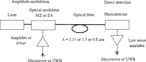
Figures 1.1 and 1.2 represent a general diagram of an IM-DD microwave optical link.
Figure 1.1. Diagram of directly modulated microwave optical link
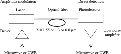
Figure 1.1 represents a direct modulation link. A laser emits a light of wavelength 0.8 or 1.3 or 1.55 µm, this laser is modulated by a microwave signal (which is possibly itself modulated) through a driver circuit. The modulated light enters an optical fiber coupled to a photodetector that detects the microwave modulation signal. The optical modulation can have an amplitude, frequency, and phase. However, direct photodetection detects only the modulation in amplitude. The detected microwave signal is then amplified by a low-noise amplifier.
Figure 1.2 represents an external modulation link. This time, a light emitted from a laser is injected into a Mach-Zehnder or electro-absorption amplitude modulator. In this case, microwave modulation is also applied to the modulator through a driver circuit.
After passing into an optical fiber, the optical intensity modulation only is detected via a photodetector. As in the previous diagram, the detected microwave signal is amplified in a low-noise amplifier.
Figure 1.2. Diagram of externally modulated microwave optical link
1.3. Signal to transmit
1.3.1. Microwave signal
The first type of transmitted signal is a signal that constitutes a microwave frequency reference. It can be used in offset aerial systems or active phased-array antenna. After its reflection from a moving object, the microwave signal emitted from an antenna can shift in frequency (Doppler modulation) and it is the spectral purity of the microwave that determines the minimum observed frequency shift and therefore, the minimum relative speed of the moving object. The spectral purity and degradation after transmission of the microwave by optical links must be watched closely to distinguish the frequency shift.
1.3.2. Microwave carrier for a digital signal
If the microwave signal serves as a carrier for a digital signal this carrier is previously modulated. All the modulation techniques normally used, such as amplitude, frequency, phase, OFDM, and combined amplitude-phase modulation (QAM), or more complex techniques can be considered, such as those used in GSM, GPRS, EDGE, and UMTS for mobile telephones or such as Bluetooth, Wi-Fi and Wimax for data transmission. These modulations are generally carried out on single sideband (SSB). When microwave signal modulation is implemented in phase or frequency, spectral purity is also of great importance.
1.3.3. UWB signal
Another signal category is available for transmission by fiber optics. These signals are relevant to UWB techniques without carriers and with the spectrum in the microwave region or up-converted to a millimeter-wave carrier. UWB wireless links are largely used over short distances. The optical fibers are particularly indicated to enable extensions of such networks.
1.3.4. Optical carrier
Microwave signals can carry analog information (frequency shift due to the Doppler effect) or they can be modulated by a digital signal or be constituted of UWB signals, which are themselves digitally modulated. All these microwave signals must be up-converted to an optical carrier. This transfer exclusively occurs by intensity modulation. One of the advantages of this modulation is that the microwave signal can be recovered in a simple photodetection unit permitting the elimination of possible frequency fluctuations of the optical carrier. Loss of sensitivity resulting from direct detection does not occur if the optical wavelength allows us to insert an optical amplifier or if the link is very short. Usually this modulation is double sideband (DSB), especially if the modulation occurs directly in the laser, but for slightly longer links this type of modulation can lead to extinction phenomena. A single sideband modulation can hence be considered, but this modulation must be carried out by an external modulator.
1.3.5. Summary
The complexity of microwave photonic links comes from the stacking of an optical carrier and microwave or UWB subcarrier. The optical carrier is exclusively intensity modulated, whereas the microwave subcarrier can be modulated following all known modulation types: amplitude, frequency, phase or their combination including a frequency shift due to the Doppler effect. All these modulations can be recovered via photodetection.
The use of microwave optical links will increase as the transmitted signals will be numerous and emitted in parallel communications and the data rates will increase accordingly. Thus, telecommunication optical networks will simultaneously transmit GSM, UMTS, UWB, and HDTV signals on different carriers. The constraints on such diverse signals will be numerous and will be emphasized in the following sections.
1.4. Limitations of microwave photonic links
1.4.1. Limitations due to the materials constituting the different elements
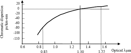
The materials used for optical fibers, such as silica or plastic substances, are characterized by losses and chromatic dispersion. The losses and chromatic dispersion for single-mode fibers (for multimode fibers the attenuation curve is identical, but is shifted higher) are presented in Figures 1.3 [COX 04; SEE 96a] and 1.4, respectively. The losses comprise two minimums at 1.3 and 1.55 μm, and chromatic dispersion is zero at 1.3 μm.
Figure 1.3. Attenuation in a single-mode silica optical fiber and functioning zones of the principal materials constituting the components of a link
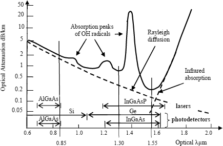
The devices used to generate, modulate, or detect optical waves, are constituted from semiconductors, and generally, comprise one or more heterojunctions, multiple quantum wells, or the stacking of different layers to create Bragg mirrors. Because of the lattice constants matching between different crystal layers, it is very easy to make these devices with AlGaAs composites on GaAs substrates. When GaInAsP or GaInAs composites are used (see Figure 1.3), stacking layers with slightly different lattice constants (constrained layers) are employed. Alternatively a more critical substrate for example, InP, is used. For the generation of an optical wave, it would be easier to design lasers with wavelengths of 0.85 or 1.3 µm rather than 1.55 µm (light-emitting diodes or LEDs are no longer used in microwave optical links) while production of 1.55 µm VCSEL lasers did not yet start.
Figure 1.4. Example of chromatic dispersion in a single-mode silica fiber
Photodetection is more feasible using Si or GaAs, which are also substrates, whereas InGaAs or Ge must be epitaxied in fine layers on a particular substrate.
For very long links, 1.55 µm wavelengths are preferred, as chromatic dispersion is the weakest between 1.3 and 1.55 µm and losses are lower at 1.55 µm. However, for short or very short links, which are the subject of this work, the attenuation per kilometer of fiber is no longer a problem and it is possible to use optical wavelengths of 1.3, 0.85, and 0.65 µm, enabling the use of low-cost VCSEL lasers and plastic fibers.
1.4.2. Noise sources in microwave photonic links
1.4.2.1. Different noises
In this section the noises affecting an optical microwave link are examined. For the electric part of the photonic link, only the thermal noise is taken into account. In the optical zone of the link it is necessary to consider the spontaneous noise emission from the laser and the shot noise from photodetectors. These noises have been modeled for many years but the explanation of their origin has only recently been presented. These aspects are only evoked as the theory involved is beyond the scope of this work [HEN 96; HEN 97].
1.4.2.2. Thermal noise
As recalled in [COX 04], this noise has been studied in two different articles published in the same journal by Johnson and Nyquist in 1928 [JOH 28; NYQ 28].
The noise corresponds to the thermal agitation of the charge carriers (electrons and holes) in the resistive parts of links, such as the resistance of the generator placed at the input, electrical losses present in all circuits, the matching resistance of Mach-Zehnder modulators, and the resistive parts of the photodetector. The corresponding signal is a random Gaussian signal, ergodic and white on a frequency range situated between 0 and kT/h (k: Boltzmann constant, h: Planck’s constant), be it from 0 to approximately 6 THz at 300K (in very low frequencies, this noise is evidently covered by 1/F noise or Flicker noise).
Figure 1.5. Representation of thermal noise in a resistance
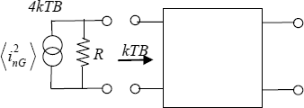
Figure 1.5 represents this thermal noise; the source is placed at the input of a two-port network (resistance R). The noise source is equivalent to a current source of internal impedance R.
The noise power available in the resistance at temperature T in a frequency bandwidth B is:
where:
k: Boltzmann constant = 1.38×10⁻²³ JK-1;
B: frequency bandwidth;
T: temperature in K.
The current source mean square value is given by:
The incident noise power at the input of the two-port network is kTB.
1.4.2.3. Quantum noise
The quantum origin of noises with spectra situated in the optical wavelength region must be taken into account in all phenomena using interactions between semiconductors and light. A very comprehensive study of these phenomena was undertaken in 1996 [HEN 96; HEN 97]. For the devices considered in this text, two cases are taken into account.
In the first case, for example a photodetector, the electrons are found in linked states. Due to the Heisenberg uncertainty principle (the position and speed of a particular particle cannot be known simultaneously), the linear momentum of these electrons fluctuates. These fluctuations of a charged particle enable the creation of a spontaneous current and, therefore, the emission of a wave. This phenomenon should induce a reduction of energy in the electrons. However, elsewhere, the quantum fluctuations of the vacuum produce electromagnetic radiation absorbed by the electrons, which compensates for the loss due to the spontaneous current. The combination of these two phenomena enables a permanent emission from the electrons into the optical spectrum. It is the beating or optical mixing of these emissions with the optical signals which generates shot noise.
In the second case, for example, that of a laser, the electrons have a high energy: they are in a position of population inversion (high energy). This time, the energy of the waves due to quantum fluctuations in the vacuum is caught and causes the transfer of these electrons from a high energy state to a lower energy state with the production of a photon. This is a spontaneous emission which is non-coherent in comparison with the stimulated emission of the laser and results in noise generated within the laser.
1.4.2.4. Shot noise
The explanation of shot noise is recent (see section 1.4.2.3), but the observation of this phenomena and the establishment of a model using photodetectors is long-standing as it was described by Schottky in 1918 [SCH 18].
Since this period, it was considered that this noise also corresponded to a random variation of current of which the effective value is proportional to the square root of the photodetected current inside the semiconductor. In terms of frequency, shot noise can be expressed in the form of current noise, of which the mean square value is:
or:
q electron charge;
ID average current in the photo detector;
B frequency bandwidth in Hz.
1.4.2.5. Dark current
In a reverse-biased photodetector, a current appears even in the absence of an optical signal. This is called a dark current. The generally accepted explanation of this current is due to ambient thermal radiation picked up by the impurity defects (deep level states) of the semiconductor [EBE 93]. The dark current (Id) mechanism also generates shot noise given by its mean square value:
1.4.2.6. Amplitude noise or RIN
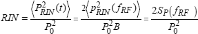
In a laser biased above the threshold, the electrons are in an inverse situation. The waves due to quantum fluctuations of the vacuum cause recombinations of these electrons and therefore spontaneous emission of photons. These photons give a random signal in comparison to the main emission of the laser, which is stimulated. This spontaneous emission can be characterized by an amplitude noise, a chirp, and by a frequency widening of the emission line. The types of photonic links described in this text are of the type intensity modulated-direct detection (IM-DD), so, frequency noises and widening of the line does not appear during detection; thus, only the intensity noise shall be taken into account (the transposition of laser 1/f noise around the microwave frequency modulation of the laser is another phenomenon specifically treated in section 6.3.4.). The parameter characterizing this noise is a relative intensity noise or RIN. Although the definitions of this RIN are different according to the reference reviewed, the expression considered in this text is that by [COX 04; ROS 98]:
In this equation, ![]() is the square average optical power at the output of the laser,
is the square average optical power at the output of the laser, ![]() is the time fluctuation of noise expressed in the power,
is the time fluctuation of noise expressed in the power, ![]() is the variance of noise measured in a frequency bandwidth B around the modulation frequency fRF of the laser modulation, SP (fRF) is the spectral noise density. RIN is expressed per hertz.
is the variance of noise measured in a frequency bandwidth B around the modulation frequency fRF of the laser modulation, SP (fRF) is the spectral noise density. RIN is expressed per hertz.
If the optical power is photodetected at the output of the laser, the noise variance and the average optical power results in an electrical current, which leads to another equation for RIN:
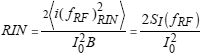
where I0 is the photodetected current corresponding to the average optical power, ![]() corresponds to the variance of the noise current at frequency fRF and SI (fRF) is the spectral noise density of current at frequency fRF.
corresponds to the variance of the noise current at frequency fRF and SI (fRF) is the spectral noise density of current at frequency fRF.
RIN can also be expressed in decibels per hertz:
It will be seen in the section on lasers that the RIN variation in terms of microwave frequency can be very strong, especially within the proximity of the laser relaxation frequency. However, the value of RIN remains constant for frequency values lower and far from the laser relaxation frequency.
1.4.2.7. Low-frequency noises
All semiconductor components introduce a low-frequency noise rise proportional to 1/f n.
As will be seen in subsequent chapters, the behavior is identical for lasers for which measurements and studies have shown the importance of low-frequency noise rise in terms of 1/f. This noise manifests itself during direct modulation of a laser by a microwave signal. It is the beating or mixing of these microwaves with low-frequency noise, which produces a frequency widening of the laser emission line and, therefore, a deterioration of the spectral purity of the phase and intensity of the microwave signal, whereas the IM-DD technique is supposed to cause no modification of the phase or frequency of the microwave signal.
1.4.3. Nonlinearities
Laser have second, third, and fifth-order nonlinearities [BIB 98] that can introduce interference in transmitted microwave signals during their direct modulation. Similarly, photodetectors, which can be either photodiodes or phototransistors, also introduce nonlinearities. These nonlinearities must be considered to characterize the complete link.
1.5. The components and characteristics of microwave photonic links
Chapters 2, 3, and 4 of this book review each component of a microwave photonic link. They consist of lasers, optical modulators, optical fibers, optical amplifiers, photodetectors, photodiodes, and phototransistors. For each of these components, the functioning and modeling principles used to carry out optimization by link simulations will be reviewed.
The useful parameters that optimize a microwave photonic link are defined and reviewed in Chapter 5. The introduction of optomicrowave S-parameters permits the definition of an amplitude and phase response for each block of the link and characterizes each component of the link. Also defined is the optomicrowave noise factor for each device, which allows characterization of the overall noise in a link. Each of these components also brings nonlinearities, characterized by classical notions of intermodulation rates and interception points. There are different sources of intermodulation and their quantification permits the definitions of an overall link nonlinearity. The combination of gains, noise factors, and nonlinearities enables the definition of an IFDR, which is necessary to enable the production of the appropriate signal to noise ratio in microwave photonic links.
Chapter 6 presents certain complementary aspects to characterize a microwave photonic link. In particular, the notion of the fading of microwave signal introduced by the chromatic dispersion of the optical fibers in the case of DSB modulation. Also presented are the different techniques producing optical single sideband (SSB) modulation and the spectral purity deterioration of a microwave signal in the case of a directly modulated laser.
Chapter 7 considers several electronic circuits placed just before or after microwave photonic links. Before the link, a modulator driver circuit is implemented for driving the laser itself or the electro-optical modulator, in case of external modulation. After the link, an amplifier is placed after the photodetector to amplify the photodetected signal with low noise.
Chapter 8 details optomicrowave component simulation techniques; models of which are presented in Chapters 2, 3, and 4. These simulations permit the characterization of complete links from the concepts developed in Chapter 5, i.e. gains, noise factors, nonlinearities, and dynamic ranges. Only these simulations enable an effective optimization of different links.