Chapter 4
Photodetectors
4.1. Photodetector definition
Regarding photodetectors, it is possible to speak of current response in units of incident optical power.
In the first English texts concerning optoelectronics, current response as a function of optical power (A/W) of a photodetector was called sensitivity. This significant term was gradually replaced by responsivity, which more specifically describes the sensitivity of a photodetector. This nomenclature will be adopted in this text.
For photodetectors, it is also possible to speak of quantum efficiency, expressed as:
with:
–np= number of electron-hole pairs generated per second;
-φ = number of incident photons per second.
The relation between quantum efficiency and responsivity Rpd in A/W is:
[4.2] ![]()
with:
– q= electron charge = 1.602×10⁻¹⁹ C;
– h = Planck’s constant = 6.626×10⁻³⁴ J/s;
ν= light wave frequency in hertz.
Responsivity takes into account the frequency of the light wave. Consequently, by referring to Table 5.1, it should be noted that for a quantum efficiency of 100%, the responsivity of an optical photodetector at 1.55 µm is 1.25 A/W, whereas to obtain identical quantum efficiency the responsivity of a photodetector at 0.8 µm is only 0.64 A/W.
In the sections below, quantum efficiency notion is used for photodiodes, while responsivity is used for phototransistors. It is nonetheless possible to go from one to the other through equation [4.2].
4.2. Photodiodes
4.2.1. Presentation
After having been transported by an optical fiber, the amplitude-modulated light flux (or Intensity Modulation) must be demodulated. Amplitude-modulated photodetection (or Direct Detection) is sufficient to detect a modulated microwave frequency or an ultra-wide band signal. This photodetection can be performed by photodiodes or phototransistors. Phototransistors shall be considered in a subsequent section, whereas photodiodes are considered below.
Optical absorption, i.e. the transformation of photons in electron-hole pairs in different semiconductors assumed to constitute photodiodes, is first considered. The varying configurations of different photodiodes will be reviewed and an equivalent electrical model to these components will be detailed. Nonlinearities and their origins will then be considered and how UTC diodes push the limits of these nonlinearities will be discussed. An outline of the different configurations allowing maximum frequency operation of these components is provided. Finally, different configurations allowing an increase in quantum efficiency are presented.
4.2.2. Light absorption in a semiconductor
Figure 4.1 represents a semiconductor block subjected to a photon flux Φ0.
Figure 4.1. Absorption of light flux in an absorbing material
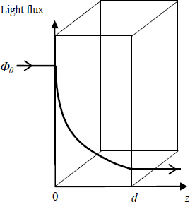
If the incident photon energies are greater than the semiconductor energy bandgap, Eg, each absorbed photon generates an electron-hole pair. The number of electrons Δn(z) hence generated as a function of penetration depth, z, in the absorbing material can be expressed [ROS 98] as:
where:
– α is the semiconductor absorption coefficient;
-LD is the diffusion length of the generated electrons in the semiconductor;
– τ is the generated electron’s lifetime.
For an absorption thickness, d, the total number of generated electrons is:
The created carrier flux is equal to Δntot /τ, it is now possible to define the photodetector internal quantum efficiency, equal to the ratio between the created electron flux and the incident photon flux:
It must be included that if the incident photons are from air, there can be a reflection at the air-semiconductor interface, in the absence of antireflection coating. In this case, if the semiconductor refractive index is nsc, the reflection coefficient is expressed:
If nsc = 3.4, then R = 0.3.
It is possible to define a quantum efficiency weighting factor due to reflection:
Giving an overall quantum efficiency:
[4.8] ![]()
Figure 4.2 gives the optical absorption coefficient of different semiconductors [GOW 93; ROS 98; SZE 91]. This figure indicates an important difference in the behavior of the absorption coefficient as a function of photon energy according to an indirect (silicon (Si), germanium (Ge), gallium phosphide (GaP)) or direct gap (the remaining semiconductors in the figure) semiconductor. The relation between photon energy and the threshold wavelength is given by expression:
where Eg is the bandgap in electronvolts.
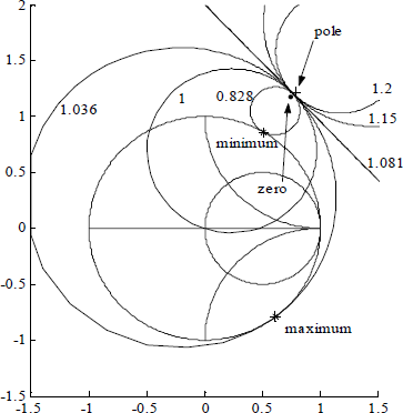
In this figure, the materials gallium arsenide (GaAs; Eg = 1.41 eV and λ = 0.88 µm) and indium arsenide (InAs; Eg = 0.36 eV and λ= 3.44 µm) appear. Between these two materials, all the ternary indium gallium arsenide (InGaAs) compounds principally allow alteration of an absorption wavelength by varying relative indium (In) and gallium (Ga) proportions. Another constraint must be considered: the lattice constant of the absorbing crystal must be identical to that of the semiconductor layers between which it is sandwiched. For example, semiconductor In0.53Ga0.47 As has a lattice constant equal to 5.87 Å, identical to InP and absorption begins at 1.65 µm. In Figure 4.2 a quaternary component is also represented (Ga0.7In0.3As0.64P0.36) whose lattice constant in the crystalline network is also identical to InP.
Figure 4.2. Absorption coefficient of different semiconductors as a function of photon energy
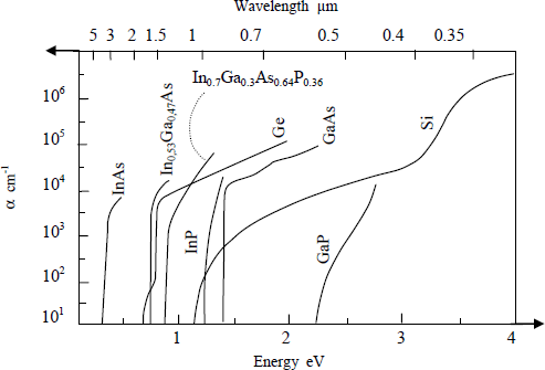
It will be seen that in a photodiode, the absorption length, d, must be as short as possible. For this, α must be very high. From Figure 4.2 an absorption layer thickness of 1 µm can be envisaged. For Si only the thickness greatly depends on the optical wavelength.
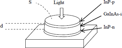
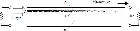
4.2.3. p-i-n photodiode
Figure 4.3 represents a p-i-n photodiode. Absorption zone (i) has a thickness, d, and a surface area, S.
Due to the limited surface area of a photodiode in comparison to the light spot surface area, the overall quantum efficiency from equation [4.8] must be multiplied by a coupling coefficient between the fiber and photodiode. This coefficient is ηc. Where the quantum efficiency expression of the photodiode is:
[4.10] 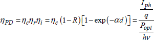
Figure 4.3. p-i-n photodiode configuration
The current generated in the photodiode as a function of optical incident power can now be written:
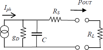
By accounting for a contact resistance, RS, and a load resistance, RL, the first equivalent electrical circuit of a photodiode can be represented, as in Figure 4.4.
In this model, the capacitance introduced by the intrinsic zone is given by expression (transition capacitance):
By considering ![]() the power delivered to the load impedance has a cutoff frequency given by:
the power delivered to the load impedance has a cutoff frequency given by:
[4.13] ![]()
Figure 4.4. Simplified equivalent circuit for a p-i-n photodiode
Elsewhere, the generated electron-hole pairs in the absorption zone are attracted by the prevailing electric field but does not instantaneously rejoin low thickness p and n zones, and hence, the photodiode electrodes.
This delay manifests itself through a transit time, inducing another photodiode frequency:
[4.14] ![]()
where ![]() is the average velocity between electron and hole velocity given by [KAT 99]:
is the average velocity between electron and hole velocity given by [KAT 99]:
For example, for InGaAs, ![]() cm/s and for d = 1µm, ft = 29.5 GHz.
cm/s and for d = 1µm, ft = 29.5 GHz.
The power delivered to the load thus has a new cutoff frequency given by:
[4.16] ![]()
or:
[4.17] 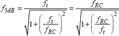
To increase the first cutoff frequency (equation [4.13]), it is possible to increase d,but if d is increased the second cutoff frequency is decreased. Only the surface area, S, of the photodiode remains undiminished, forcing a size reduction of the optical fiber light spot. This dimension, however, cannot be indefinitely reduced. The coupling term of the photodetector quantum efficiency (ηc from [4.10]) is hence reduced. Additionally, as photodetection volume is also reduced this limits photodetection power, as seen further on. The design requirements of a p-i-n photodiode consist of finding a compromise between the different constraints outlined above.
By combining equations [4.13], [4.14], [4.16], and [4.17], it is possible to establish the following equation [CAB 03a]:
[4.18] 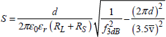
In this equation it can be seen that for a given frequency f3dB, the diode thickness d must respect:
For example, with GaInAs:
–εr = 13.6
–vnsat = 6.5×106 cm/s
–vpsat = 4.8×106 cm/s
![]() cm/s
cm/s
If f3dB must be 60 GHz, d < 0.497 µm. By d = 0.4 µm and RS + RL = 60 Ω, equation [4.18] gives a surface area of S = 87 μm2, or a photodiode diameter of 10.5 µm.
For example, at the output of a simply cleaved fiber a luminous spot of approximately 16 µm in diameter appears and at the output of a lens fiber a spot of 4 µm appears.
With the above values, ft = 73.8 GHz and fRC = 101GHz. And by considering that α=104/cm (λopt = 1.5 µm), the internal quantum efficiency of this photodiode is ηi = 1 − exp(−αd)= 0.33.
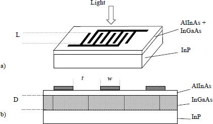
4.2.4. Metal-semiconductor-metal or MSM photodiode
The configuration of such a diode is given in Figure 4.5a. The black parts are metallic electrodes on a semiconductor. This is known as aSchottky junction. An applied voltage between each of the electrodes always arrives at one of the junctions reversed. Figure 4.5b shows a transverse cross-section representing three fingers of Figure 4.5a. A fine layer of AlInAs is deposited to assure good diode operation without reverse current. The light absorption zone is the InGaAs layer.
Figure 4.5. Metal-semiconductor-metal (MSM) photodiode
As for a p-i-n photodiode, it is possible to define an inter-electrode capacitance given by expression [CAB 03a]:
with:
– N number of electrode fingers from Figure 4.5a;
–ε0 permittivity of free space;
–εr relative permittivity;
-L finger length;
k’ parameter defined by: k’=1 − k2 with ![]() where w is the thickness of the finger and t is the distance between the two.
where w is the thickness of the finger and t is the distance between the two.
It is also possible to define a cutoff frequency due to carrier transit time in the layer as in equation [4.14] by assuming d [KAT 99] is:
where D is the thickness of the absorbing layer.
With these values of d and C, the same cutoff frequencies as the p-i-n photodiode can be calculated and the same reasoning can be maintained on the compromise between different dimensions.
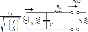
4.2.5. Equivalent circuits for p-i-n and MSM photodiodes
It is now possible to propose in Figure 4.6, an electrical model to p-i-n or MSM photodiodes. This diagram gives a cutoff frequency at -3 dB of the power in the load identical to those given by equations [4.16] and [4.17].
Figure 4.6. Equivalent circuit for p-i-n and MSM photodiodes
4.2.6. Nonlinearities
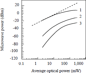
It was seen in the previous section that to operate at high frequency a p-i-n photodiode must have low absorption thickness and surface area. As a consequence nonlinearities appear for photodiodes operating at very high frequencies and submitted to high-power light sources. For a p-i-n photodiode, these nonlinearities were observed by measurement and then simulated [DEN 90].
Figure 4.7 represents the simulated response of an InP/GaInAs/InP p-i-n photodiode with an absorption thickness of 1.5 µm and a surface area of 400 µm2, or a diameter of 22.5 µm. Its cut-off frequency at -3 dB is 22 GHz [HAR 96]. The results are obtained with a 100% microwave modulation and a continuous biasing voltage of -2 V. The curves represent the response in fundamental frequency at 20 GHz (1), second (2) and third-order (3) harmonics. These curves demonstrate that even with a low cutoff frequency photodiode, nonlinear effects are no longer negligible above a few milliwatts of optical power. These results considerably limit the use of photodetectors, in particular when there is a design requirement for part of the amplification to take place as optical amplification before photodetection in a microwave optical link.
Figure 4.7. p-i-n photodiode nonlinearities [HAR 96]
Photon absorption in the absorbing region of a photodiode creates electron-hole pairs. Under the effect of a reverse voltage applied to the diode and so from the electric field appearing in zone i, the electrons are directed towards zone n and the holes towards zone p. These charges create a space charge region generating an electric field (see Poisson equation) that can interfere with the electric field due to reverse voltage. This new, weaker electric field delays carriers and possibly reinforces the depletion zone. This screening phenomenon of the electric field by the space charge and hence carrier delay is the principle cause of nonlinearities in a p-i-n photodiode. In reality, the possible causes of nonlinearities in such a photodiode are numerous and systematic studies comparing measurements and simulations have been performed [WIL 96]. These results led to design rules for p-i-n photodiodes by optimizing the maximum received optical power and hence the microwave power produced [WIL 99]. This design process is outside the scope of this work. It is sufficient to note the values considered, which are the absorption zone thickness and diameter as a function of optical wavelength and, especially, the detectable microwave frequency, the photodiode biasing voltage, the residual doping of zone i, the importance of having non-absorbing zones (p and n), the face of the incidence of the optical wave (zone p or n), thermal effects, the eventual influence of load resistance, etc.
4.2.7. UTC photodiodes
One particular photodiode configuration enables the reduction of space charge, which is the main source of nonlinearity. This configuration is represented in Figure 4.8 [ISH 00; KAT 99].
Figure 4.8. UTC photodiode energy diagram
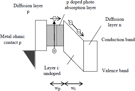
The principle of this photodiode is based on the fact that photo-absorption (small gap) occurs in p-doped zones followed by large gap i zones. As in p-i-n photodiodes, these two zones are framed by the large gap zones p and n. Photo-absorption generates electron-hole pairs. In all semiconductors the holes generated in zone p are absorbed in this same zone with a very short relaxation time. However, the electrons move via diffusion into zone p towards zone i where they are captured and drift under the effect of the electric field present in this zone. Hence the space charge in zone is only due to electrons. Additionally, as long as the layer has a thickness that is less than 0.2 µm, a velocity overshoot phenomenon occurs (see Appendix, section 4.4.2) meaning that the electrons can move at five times their saturation velocity. As a result, this reduces (by a factor of five) space charge in zone i. In these photodiodes, the transport only takes place with a single carrier, so they are called uni-traveling-carrier (UTC) photodiodes.
Regarding transit time, the path of velocity overshoot electrons in zone i is very short and the diffusion path in zone p is longer. Hence by compensation, a UTC diode is, in principle, no faster than a p-i-n diode. The absorption zone velocity can, however, be increased by introducing gradual doping creating an electric field and hence accelerating electrons. As a result, UTC photodiodes can be very fast [ISH 00].
Results obtained with these photodiodes indicate a 1 dB (nonlinearity) compression of photodetected current three-times superior to p-i-n photodiodes. However, the comparison is difficult as the presented values refer to a pulse operation, eliminating thermal effects, which must also be taken into account to analyze all nonlinearity sources. A photodiode with a gradual doping absorption zone of 0.14 µm and a zone i of 0.2 µm shows a cutoff frequency of 114 GHz. In any case, to attain such frequencies, thin absorption thicknesses are necessary and quantum efficiencies remain low; 13% in the example above [KAT 99].
4.2.8. Charge compensation
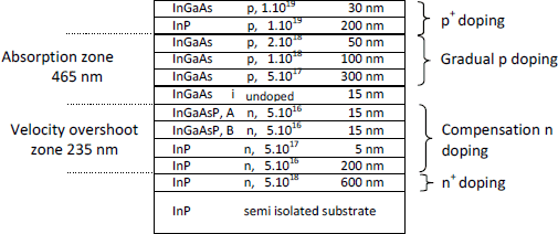
In a UTC photodiode, the space charge region appears at a much higher current than for a p-i-n diode, but it appears nonetheless. It has been proposed to compensate these charges by partially replacing undoped zone i by a slightly doped zone. This is made possible by noting electron velocity and velocity overshoots are not affected as long as the doping is ≤1×10¹⁷/cm3.
Figure 4.9 shows the layers of an InP/InGaAs UTC photodiode [LI 04] with a n charge compensation as well as a gradual p profile in the absorbing zone. The two InGaAsP layers are placed to soften the barrier height difference between In0.53Ga0.47As and InP. The gap size of layer A corresponds to a wavelength of 1.3 µm and that of layer B to 1.1 µm (for In0.53Ga0.47As, λEg = 1.65 µm and for InP, λEg = 0.92 µm). The doping of 5×10¹⁷/cm3 over 5 nm in zone n has the effect of increasing the electric field in this zone. With such a structure (20 µm diameter), current saturation begins at 90 mA, corresponding to a microwave power of 20 dBm at 20 GHz.
Figure 4.9. Space charge compensation UTC photodiode
4.2.9. Partially depleted absorption zone
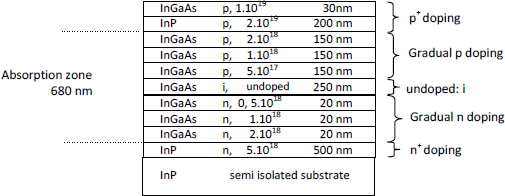
Another technique to minimize nonlinearities is to thin the undoped zone to reduce the voltage necessary to bias the photodiode. This reduces the electrical power, which must be dissipated by the photodiode; the InGaAs semiconductor is a particularly bad thermal conductor. Figure 4.10 shows the division between the different layers of such a photodiode [LI 03a; LI 03b].
This time the p-i-n photodiode has a thicker absorbing zone (0.68 µm) associated with an undoped zone of a three times smaller thickness. When illuminated from the back, this photodiode has a current of 24 mA at a 1 dB compression of the generated microwave power at 50 GHz for an applied voltage of 2.7 V.
Figure 4.10. Partially doped absorbing zone p-i-n photodiode
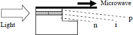
4.2.10. Lateral lighting
To improve light absorption, a solution is to laterally couple or edge-couple light in a p-i-n photodiode. This configuration is called a waveguide photodiode. Figure 4.11 illustrates this type of device.
Lateral lighting guarantees a good absorption in the photodiode zone but difficulties arise from lateral injection. As a result, the thickness of zone is always inferior to 1 Jim; however, the diameter of a lens fiber is 4 Jim and can be reduced to 2 Jim with several lenses, but never less [KAT 99]. In this type of device, the coupling losses will always be large.
Figure 4.11. Lateral lighting of a p-i-n diode
Elsewhere, the increase of operational frequencies of these photodiodes leads to a reduction of the thickness of the absorbing zone to reduce transit time, leading to a reduction of electrode surface area, increasing contact resistance, and hence, series resistance of the equivalent circuit of Figure 4.6. The arrangement proposed in Figure 4.12 prevents several of the above effects [KAT 96].
Figure 4.12. Lateral lighting of a p-i-n diode: mushroom structure
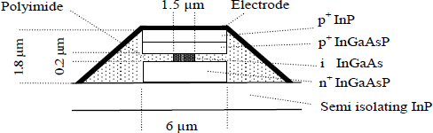
Firstly, the height of the structure for insertion of the optical wave is increased by adding two layers of InGaAsP matched in terms of the lattice constant (see Appendix, section 4.4.1), which do not absorb light but guide it between the two InP layers (this structure is called a double core). These layers, as well as the InP layer, are sufficiently enlarged to reduce photodiode contact or series resistance. The hollow parts are then filled with polyimide, which has a very low dielectric constant in comparison with InGaAsP, which enables a decrease in the photodiode transition capacitance.
4.2.11. Lateral lighting: progressive wave structure
From lateral lighting, the structure of the photodetector can be a transmission line. In this line, the optical wave propagates whilst being progressively attenuated, whereas the photodetected electrical wavelength propagates up to a load, RL. Figure 4.13 shows this configuration.
Figure 4.13. Lateral lighting of a distributed structure p-i-n diode
In the p-i-n photodiode considered to be a line, electrical wave propagation velocity and characteristic impedance of the line are given by the classical relation of transmission lines [GIB 97; KAT 99]:
[4.22] ![]()
[4.23] ![]()
where Lu and Cu are the line network inductances and capacitances per unit length of the photodiode electrode. The line network capacitance can be expressed as:
[4.24] ![]()
where:
w is the line width;
d is the thickness of the absorbing layer.
By combining equations [4.22], [4.23], and [4.24], the electric wave propagation velocity is:
In the case of an InP/InGaAsP/InGaAs /InGaAsP/InP photodiode of thickness d of 0.2 Jim, frequency ft is 150 GHz. Electric wave propagation velocities are 3.3×109 cm/s for w = 1 Jim and 1.65×109 cm/s for w = 2 Jim. The optical wave propagation velocity is 8.1×109 cm/s. So the electrical wave propagates at a lower velocity than the optical wave. These velocity differences introduce frequency limitations. It would be best to use a width w of 1 Jim because the coupling efficiency decreases with decreasing values of w. Considering a spot with a diameter of 1.3 Jim (a slightly lower value than above) and a double core thickness of 1.8 Jim, the width of 1 Jim has an efficiency of 45% and the width of 2 Jim has an efficiency of 70%. So a higher bandwidth comes at the cost of a coupling efficiency loss.
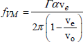
Another limitation comes from the fact that photodetection generates an electric progressive and an electric regressive wave [GIB 97; KAT 99]. The progressive wave is absorbed by load resistance RL. However, if no electric load is placed at the optical input (see Figure 4.13), the regressive wave is reflected and returns in the progressive direction but without phase coherence with the first progressive wave. This also damages the bandwidth. If a matched load is placed at the input, this increases operational frequency but suppression of one of the two waves reduces internal efficiency by 50%. The frequency limit due to a zero resistance velocity gap at the input is expressed as:
where:
− Γ is an optical confinement factor;
− α is an absorption coefficient;
− ve is the electrical wave velocity;
− fVM is the cutoff frequency due to the velocity differences (velocity matching).
While in the presence of input resistance, the expression used is:
where vo = optical wave velocity.
If α is high enough, this frequency can be high, but in the opposite case, it is evident it is more beneficial to have an input load.
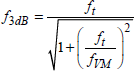
By accounting for the frequency due to mismatching, the device cutoff frequency at -3 dB is finally given by:
To summarize, this type of structure offers the advantage of total absorption of an optical wave without impairing the maximum operational frequency.
An example of such a structure operates at an optical wavelength of 0.83 µm. The GaAs p-i-n photodiode has a width of 1 µm and a length of 7 µm. This photodiode has a bandwidth of 172 GHz and an efficiency of 42% [KAT 99].
4.2.12. Lateral lighting: periodic structures
It was seen in the previous section that for a progressive wave structure, one of the difficulties comes from the mismatching of optical progressive and photodetected electrical wave velocities that propagate on the same line.
The principle of periodic structures consists of decoupling the two waves in such a way as to match the two velocities. Hence, the general term for designing these structures is velocity-matched distributed photodetectors (VMDP).
The different structures allowing this velocity matching are discussed in [KAT 99]. An example of such a realization is given in Figure 4.14 [LIN 96; LIN 97]. A dielectric waveguide guides the light. Along the length of this waveguide, photodiodes are arranged and the photodetected microwave signal is transmitted along a planar transmission line with a characteristic impedance of 50 Ω. The phase velocity along this line is reduced, in such a fashion as to stall that of the light velocity in the dielectric guide by loading it with a capacitance. In the example given in [LIN 96], the photodiodes are MSM diodes (see section 4.2.4) and it is hence the capacitances of these diodes which load the line.
Figure 4.14. Periodic structure photodetector
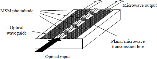
Figure 4.15 illustrates the optical waveguide of width 3 µm and MSM photodiodes.
Figure 4.15. Periodic structure photodetector: waveguide and MSM diode
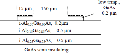
The guide optical confinement is ensured by the stacking of AlGaAs differently composed layers and hence of different dielectric constants. This stacking is realized with AlGaAs as the lattice constants of the different compounds are the same (see Appendix, section 4.4.1), it would be impossible with other semiconductors. The absorption in MSM diodes occurs in a GaAs layer epitaxied at low temperature.
The theoretical analysis of this structure [LIN 97] performed for a wavelength of 0.86 Jim, shows that as in distributed structures, a load resistance must be placed at the input in order to have a large bandwidth response, and thus, this limits quantum efficiency. Similarly, the coupling between the optical fiber and optical waveguide introduces losses as the optical guide height is low. Regarding the periodic line structure, the maximum frequency is limited to approximately 100 GHz. With this structure, it is possible to foresee a bandwidth of 80 GHz from eight photodiodes (four in Figure 4.14).
4.2.13. Resonant optical cavity photodetector
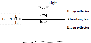
This type of configuration consists of inserting the photodetector in a vertical optical cavity, delimited by Bragg reflectors, comprising layers of materials with different dielectric constants. The principle of these resonant cavity-enhanced (RCE) photodetectors is shown in Figure 4.16.
One of the first realizations of placing a phototransistor between two Bragg reflectors occurred in 1990 [UNL 90]. A second example happened with a p-i-n photodiode [BAR 94], a third example was based on a Schottky photodiode [ONA 98], and a fourth example was realized with an avalanche photodiode [LEN 99].
The theory of this device type was explained in 1991 [KIS 91]. The general topology is that of Figure 4.16 from which the quantum efficiency of such a photodetector is expressed by the following expression given without demonstration:
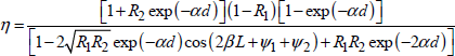
where:
– R1 and R2 are the reflection coefficients of superior (R1) and inferior (R2) Bragg reflectors;
– αd corresponds to the attenuation in the absorbing zone;
– L is the cavity length;
– β = 2πn/λ is the propagation constant in the cavity, with n, refractive index of cavity material and λ, the wavelength;
–ψ1, ψ2 are the Bragg mirrors phase shifts.
Figure 4.16. Resonant optical cavity-enhanced photodetector
An example calculation of η, for wavelengths between 0.88 and 0.96 Jim, is given for a GaAs cavity (n = 3.6) of length L = 2.39 Jim, an absorbing zone αd = 0.1 and Bragg reflectors defined by R2 =0.9 and R1 corresponding to three different values, 0.05, 0.3, and 0.9. Following the work of [BDE 06], ψ1 and ψ2 values are approximated by a penetration depth Lpen =λ0/4 with λ0 = 0.92 μm. Figure 4.17 gives the results of this simulation and presents the characteristics of such a device.
Insertion of the photodetector device in an optical cavity considerably improves quantum efficiency. For this, quantum efficiency of a single optical wave (1-exp(-αd)) as shown in Figure 4.17 must be compared.
Figure 4.17. Optical cavity photodiode quantum efficiency for R2 = 0.9 and αd = 0.1
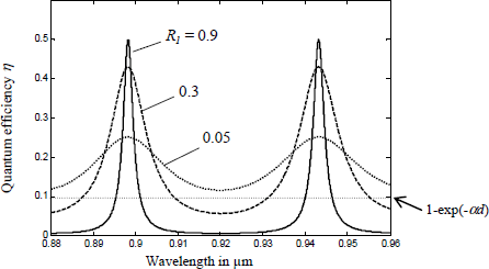
Efficiency can be increased by adjusting the reflection coefficients of the Bragg reflectors, by making R2 tend towards 1 and adjusting the R1 reflection coefficient in relation to R2. This efficiency is particularly maximized if:
In these conditions, the cavity Q_factor is increased and the resonance becomes increasingly acute. This aspect can be considered a disadvantage because the photodiode no longer operates in a wide optical bandwidth. This can also be an advantage for use in a multi-wavelength optical system (WDM systems) through its wavelength selectivity aspect.
4.2.14. Diluted waveguides and evanescent mode coupling
To improve the coupling between the optical fiber and photodiode, and hence the quantum efficiency, a number of structures have been considered ranging from SiO2 joints that electrically separate the optical waveguide and photodiodes (butt-joint) [KAT 92] to tapered optical waveguides [DEM 01]. Only the configuration producing the best results will be presented below. The chosen configuration consists of a diluted optical waveguide associated with an evanescent mode coupling.
The presented structure consists of coupling the optical wave from a fiber with a p-i-n photodiode. Figure 4.18 illustrates the structure [DEM 03].
Figure 4.18. Coupling to a photodiode with a diluted waveguide and evanescent waves
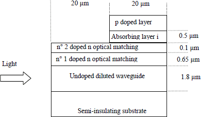
The diluted waveguide was proposed to increase the height of the light ray (dilute) emitting from a laser [CHO 94]. The reciprocating principle starts from a thick guide and arrives at a lower height. However, height reduction is achieved by an evanescent coupling between the guide and active zone of the photodiode. In the example presented here, the diluted waveguide is a planar guide constituted from a stack of a number of 10InP/GaInAsP layers where the GaInAsP layers are adjusted to give an energy gap corresponding to λEg = 1.1 µm. The InP and GaInAsP thicknesses are 100 nm and 80 nm respectively, or have a guide height of 1.8 µm. The coupling towards the photodiode is then assured by two optical matching layers. The first is a GaInAsP layer (λEg = 1.1 µm) 0.65 µm thick (refractive index of 3.28) and the second is a GaInAsP layer (λEg = 1.4 µm) 0.1 µm thick (refractive index of 3.45). The n doping of these two layers, fixed at 1018/cm3, slightly reduces the refractive indices. The InGaAs absorbing layer (0.5 µm) is not doped. The length of the p-i-n diode is 20 µm and the width is 5 µm.
The measurements performed with such a device show a microwave bandwidth of 48 GHz and a quantum efficiency of 82%.
4.2.15. Summary
The abovementioned different steps to improve photodiode performance can be summarized as follows.
To attain a high microwave frequency, the transit time must first be diminished. For this, the zone thickness situated between p+ and n+ layers of the diodes must be reduced. To obtain high frequencies, the diode surface area must be reduced in order to reduce the parasitic capacitance and so the time constant (the load R is generally 50 Ω).
Current induced in photodiodes creates a space charge region and hence nonlinearities even for low-power microwaves. These nonlinearities can be diminished by optimizing the repartition between the absorption and transit zones (UTC diode, charge compensations or partially doped absorption zone diodes).
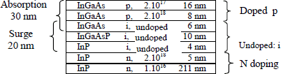
The application of the three steps above is well presented in the results of [ITO 00], which concerns an UTC photodiode with a bandwidth of 310 GHz. Figure 4.19 shows the different constituent layers of this diode. The transit zone has a total height of 44 nm. The capacitance constituent zone (zone i) has a height of 20 nm and the photodiode surface area is 50 µm2. Finally, the charge accumulation zone volume is only 1 µm3, but the UTC structure maximally reduces nonlinearities.
It was recalled that the ratio between the current detected by a UTC photodiode and the current detected by a p-i-n photodiode is 3, or approximately 10 dB in power, but from 100 GHz, the current ratio increases to 10 dB and the power ratio attains 20 dB [NAG 09].
Concerning quantum efficiencies, the first step is to edge-couple the light to the photodiodes and to use distributed structures where different optical and electric wavelength velocities limit frequency increase. In this direction, the optical (in a dielectric waveguide) and electrical wave (in a localized transmission line) separation allows the increase in frequency while conserving good quantum efficiency. However, the obligation to load a matched impedance at the input of the microwave line limits quantum efficiency to 50%.
To increase quantum efficiency two other possibilities are available:
- inserting photodiodes between Bragg mirrors increases quantum efficiencies up to 90%, but at the price of a very high wave selectivity. This inconvenience can become an advantage, as in wavelength division multiplexing systems (WDM);
- using diluted waveguides and evanescent couplings. In this case, quantum efficiencies stay high and the optical wavelength detection range is certainly the largest.
Figure 4.19. UTC photodiodes at 310 GHz
Another remark must be made: all the studies presented in this section have required numeric simulations. To optimize the different photodiode semiconductor layers, simulators must account for complex relations giving carrier velocities as a function of electric fields but also giving velocity overshoots. For optical waveguides, the simulators must be capable of treating optical propagation, and in three-dimensions [ATL].
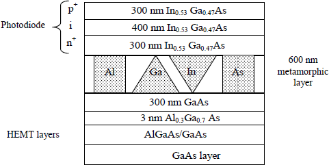
To recall, InP/InGaAs/InP (1.55 µm) photodiodes were realized on HFET (or HEMT) AlGaAs/GaAs technology. To make this technology compatible, a metamorphic layer is inserted between HFET and photodiode technologies (see Appendix, section 4.4.1.3). Examples of such achievements are featured in [HUR 97] and [JAN 02].
4.3. Phototransistors
4.3.1. Bipolar or field-effect phototransistors?
For all the successful transistor configurations since the invention of the point contact transistor in 1948, the problem of interaction with light was always an issue [SZE 91]. Concerning high frequencies, a frequency response comparison of different microwave transistors showed they do not all behave in the same manner when lit by a modulated optical source [BAR 97].
For example, heterojunction field-effect transistors (HFET, HEMT, TEGFET or MODFET) with a gate of 0.25 µm-length and a fT of 58 GHz, lit by a modulated optical source, produce a photovoltaic current with a cutoff frequency inferior to 20 MHz and a photoconduction current with a cutoff frequency in the order of 1 GHz, but with a lower amplitude of 16 dB. For a metal semiconductor field-effect transistor with a gate of 0.25 µm and a fT of 20 GHz, the photo-conducting current has a cutoff frequency of a few gigahertz, but a lower amplitude of 55 dB, less than the photovoltaic current! So, concerning the optoelectronic response, the MESFET and HFET cannot be considered as microwave phototransistors.
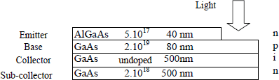
Conversely, bipolar transistors have long been known to be good phototransistors [SZE 81]. In microwaves, a heterojunction bipolar transistor (HBT) must be used. For example, for a n-p-n HBT (structure illustrated in Figure 4.20), with a light window of 1.5×10 µm2, the optical response has the same frequency behavior as the electrical response. The HBT is hence a good candidate to be a microwave phototransistor. These transistors are called heterojunction phototransistors (HPT).
The comparison between field-effect transistors and bipolar transistors can be summarized in the following manner. During the lighting of a field-effect transistor, the photovoltaic photocurrent is no longer amplified whereas in a bipolar transistor, all currents injected into the base are amplified by the transistor. It is this behavior that explains the considerable differences in the lighting effect between a field-effect transistor and a bipolar transistor.
By recalling that for the short links studied in this work and as a function of optical fibers used, the optical wavelengths range from 0.6 to 1.55 µm, and in terms of realization difficulties, different HPTs are possible.
The chronological order of HPT realization is as follows: GaAlAs/GaAs or GaInP/GaAs (absorption in GaAs below 0.85 µm), InP/InGaAs (absorption in InGaAs from 1.55 µm) and Si/SiGe/Si (progressive absorption in constrained SiGe below 1.2 µm).
Figure 4.20. HPT structure
Generally, in such a transistor, the base-collector-sub-collector behaves as a p-i-n photodiode (see Figure 4.20) and injects the photodetected current between the base and collector. In all bipolar transistors, a current injected via the base is amplified. A phototransistor can hence be represented by the simplified diagram of Figure 4.21 [SZE 81].
Figure 4.21. Simplified diagram of a HBT
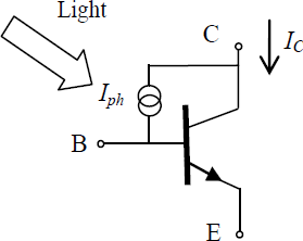
The current IC in such a transistor can be written:
where hFE is the transistor current gain.
As the current gain of a transistor can be very high, this relation shows the benefit of using a phototransistor over a photodiode, which only generates Iph.
The Appendix presented in section 4.4.3 succinctly recalls the main characteristics of a microwave HBT.
4.3.2. GaAlAs/GaAs and InGaP/GaAs phototransistors
The first HBTs were realized on GaAs substrates because AlGaAs/GaAs heterojunctions have lattice matching regardless of the proportion of Al and Ga (see Appendix, section 4.4.1). Elsewhere, the GaAs substrate was very rapidly available in the form of wafers with good mechanical and electrical properties. The GaAs semiconductor only shows a correct absorption for wavelengths inferior to 0.85 µm. Several articles evoke the possibility of using HBTs [BAR 97]. The first measurements of AlGaAs/GaAs phototransistors showing microwave performances appear to have been presented in [SUE 93].
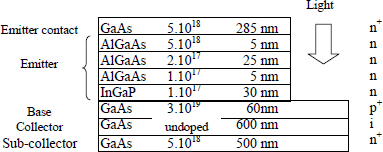
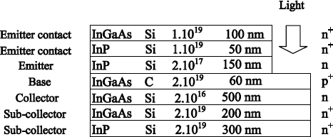
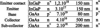
A first example of a GaAs phototransistor is the GaAlAs/GaAs transistor discussed in the introduction. The different semiconducting layers of this transistor are recalled in Figure 4.20.
A second possibility consists of replacing all or part of the GaAlAs (wider bandgap semiconductor) of the emitter by InGaP (in reality, In0.48Ga0.52P), also a large bandgap semiconductor. The technological reason of this substitution is given in section 4.4.3. As a result of a window placed either between the base and the emitter contacts or directly in the emitter contact, the light must be sent from above for GaAs transistors.
A comparison of these two window types was performed in [KAM 94]. In this reference, despite the title, the transistors used are InGaP/GaAs [YAM 94] but also including a layer stacking of AlGaAs. Hence, it is a little different from the transistor in section 4.4.3. The stacking is illustrated in Figure 4.22.
Figure 4.22. Stacking of the AlGaAs/GaInP/GaAs phototransistor layers [YAM 94]
The dimensions and disposition of windows E/B and E are explained in Figure 4.23 and the values of x are given in Table 4.1.
Figure 4.23. Phototransistor windows forms and dimensions from Figure 4.22. The dimensions are in µm
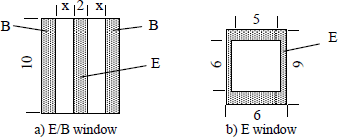
Table 4.1 summarizes the microwave performance of four transistor types from Figures 4.23a or 4.23b following a biasing at VCE = 2 V and IC = 6 mA and S-parameters measurements. It is obvious from this table that the presence of an optical window reduces microwave performance in relation to the RF transistor when the input signal is applied to the base. This is found on fT (increase of CBE, not indicated in the table) and on fmax (increase of RB and CBC).
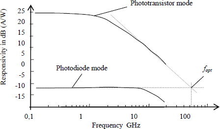
However, when these transistors are lit by a 0.83 µm optical wave modulated by a frequency of 20 GHz, the optical gains, tens of dB, are the same for the four transistors. It is the same for the optical cutoff frequencies (see Figure 4.26 for the evaluation of this frequency). The optical gain is defined as the ratio of the transistor mode photodetected microwave power to the photodiode mode photodetected microwave power, junction B-E being short circuited in this last case.
Table 4.1. Microwave performance of different GaAs phototransistors
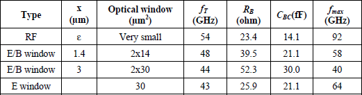
Similarly, signal/noise ratio measurement gives the same results for the four transistors, whereas the Fukui formula [4.51] shows that an increase of RB should reduce noise.
The two results above explain themselves because the optical wave is applied as near as possible to the transistor, whereas the microwave signals applied to the base have a resistance larger than the optical window.
Elsewhere, the signal-to-noise ratio shows an improvement of about 5 dB in transistor mode despite a gain of 10 dB in comparison to the photodiode mode. This demonstrates the benefit of using a phototransistor.
Finally, the window form and dimensions depend on the light spot, which enable lighting of the phototransistor. If this spot has a diameter of 5 Jim, the window placed in the emitter is quite beneficial. However, if the spot has a larger diameter (e.g. 10 μm), it is better to use an E/B window type.
4.3.3. InP/InGaAs phototransistors
Light absorption takes place at optical wavelengths equal or inferior to 1.55 μm, whereas for the photodiodes, an arrangement of InGaAs material with good proportions of Ga and In must be present. This is obtained by realizing InP/InGaAs heterojunctions on an InP substrate. For lattice match to occur, the material used is actually In0.53Ga0.47As. This also corresponds to a good absorption coefficient at 1.55 μm (see Figure 4.2).
Several InP/InGaAs phototransistor combinations have been proposed but without any possibility of base contact. To obtain good microwave performance, base contact is useful for improved biasing [CHA 91] but also, as shall be seen, on optimal base impedance. The likelihood of InP/InGaAs phototransistors performance for large wavelengths was predicted in 1982 [CAM 82].
An example of such a transistor is detailed below. It was first realized with a uniform base [GON 03], then with a gradual base [THU 99]. The two gave rise to simulations [CHE 99].
The uniformly doped base phototransistor is represented in Figure 4.24. The vertical white line on the electron microscope photo (b) represents a vertical 10 µm length. Horizontally the image is a little distorted. On this photo, the base and sub-collector emitter contacts can be seen and correspond to the metallic contacts on the phototransistor cross-section (a). The emitter has a surface area of 4 × 3.5 µm2 and the optical window has a surface area of 5 × 6 µm2.
Figure 4.24. Simple InP/InGaAsheterojunction phototransistor
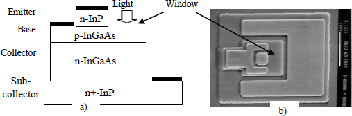
Figure 4.25 illustrates the materials, the heights of the layers, and the intrinsic transistor doping. Several base profiles are considered. Only the results of the best profile, in other words the base profile, are considered. The gradual aspect of this base appears in the variation of its composition: it goes from In0.53Ga0.47As at B/C level to In0.46Ga0.54As at E/B level. The gradual base aims to produce an electric field in this base and hence increases electron velocity. The nature of the doping agents is also featured in this figure.
The electrical and optical measurements were carried out by biasing the transistor at VCE = 1.6 V and ICE = 10 mA. In these conditions, fT = 71 GHz. The optical measurement is carried out at 1.55 µm with an optical power of 0.7 mW and a modulation index of 50%. The optical response is represented in Figure 4.26.
Figure 4.25. Layers of the simple heterojunction phototransistor of Figure 4.24
This figure represents the phototransistor optical frequency response, which can be obtained through measurement [THU 99] or by simulation [CHE 99]. For this transistor, the cutoff frequency is 52 GHz.
Figure 4.26. Optical response and evaluation of the optical cutoff frequency
An initial improvement consists of positioning a 100 nm InP layer as a sub-collector. This constitutes a second heterojunction and this transistor is considered as a double heterojunction transistor [KAM 95a]. This heterojunction blocks the holes photodetected by the sub-collector, which slows the transistor, but the 330 nm of collector under the base is in InGaAs. This is essential to have a good optical absorption signal; however, the remaining photodetected holes always slow the transistor. This type of transistor has a cutoff frequency of 82 GHz [KAM 00].
For the above transistors, the photodetected structure is composed of the base and collector layers. This collection associated with the sub-collector has a p-i-n diode configuration. The holes generated in the depleted zone of the collector must rise towards the base, which increases the transit time. One solution is that photodetection takes place only in the base and the collector is made of a wider bandgap material, as in UTC diodes. If the transit time in the base remains short, this should accelerate transistor response speed.
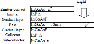
This is proposed in the phototransistors described in [KOP 98] and [KOP 00]. Figure 4.27 illustrates the different materials. Even if the dimensions do not appear on these figures, the base is sandwiched between two heterojunctions. The abrupt change of gap height is attenuated by two gradual layers of quaternary compounds.
Figure 4.27. Double heterojunction transistor structure
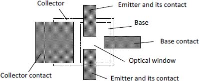
With the HBT technology currently in use, a phototransistor was realized [LEV 03; LEV 04] according to the simplified drawing of Figure 4.28. In this drawing it appears that a window of 2.6 × 3 µm2 was opened in the transistor emitter with a dimension of 2.6 × 7.8 µm2. To better understand its design, the height difference between the collector, base, and emitter are smoothed by glass encapsulation [KOP 98].
With this phototransistor, an optical cutoff frequency of 135 GHz is obtained for VCE = 2 V and for an optimal value IB between 0.1 and 1 mA. The optimum ft and fmax are 130 and 100 GHz, respectively. Whereas a HBT transistor with an emitter of 1.2 × 7 µm2 performs ft = 150 GHz and fmax = 220 GHz. The first disadvantage of this transistor is absorption in the base causing very low (0.08 A/W) responsivity. The second disadvantage comes from the limitation of fmax due to the necessity to open a window of reasonable dimensions in order to have consequent absorption in the base, causing a high value CBC capacitance.
Double heterojunction InP/InGaAs bipolar transistors are hence good candidates as phototransistors. Amongst these, a HBT with aft of 290 GHZ [GOD 08], used as a phototransistor but for which fopt is still unknown must be mentioned. To improve phototransistor fopt, a solution is to edge-couple light in the phototransistor [DUP 03], but what is gained in absorption is partly lost during optical wave coupling with the only base.
Figure 4.28. Simplified drawing of a base-collector heterojunction phototransistor
Another solution consists of lighting the phototransistor via an optical guide passing below the sub-collector. This was realized by [HOU 06]. The technology is the same as that evoked above but an InGaAlAs layer constitutes a waveguide passing below the sub-collector and removes the need for a window in the emitter.
Figure 4.29 represents the arrangement of the layers so that it can be deduced from [HOU 06].
The adopted arrangement considerably reduces phototransistor dimensions. The first phototransistor has an emitter of 0.7 × 4 µm2. For a biasing VCE = 1.5 V, IC = 12 mA, IB = 0.65 mA, ft and fmax are 204 and 203 GHz, respectively. Optically, the low frequency optical gain is 33 dB and the optical cutoff frequency fopt is 447 GHz.
Figure 4.29. Layers of a double heterojunction phototransistor with an optical guide
A second phototransistor has an emitter of 0.7 × 16 µm2. For this second transistor, for a biasing of VCE = 1.5 V, IB = 2.4 mA, the optical gain is 38 dB and the optical cutoff frequency, fopt, is 340 GHz.
The emitter window reduction results in a considerable increase in the optical cutoff frequency above electrical ft and fmax as would be expected from the first phototransistor evaluations. This was obtained through a drastic reduction of emitter dimensions and thus responsivity of the phototransistor. The first of these phototransistors (fopt = 447 GHz) has a responsivity of 0.05 A/W, which is very small. The second transistor (fopt = 341 GHz) has a responsivity of 0.2 A/W, which is 2.5 times better than the phototransistor from Figure 4.28 for a clearly higher fopt.
It is best to remove the lighting window on the emitter, leading to a reduction in component dimensions and thus an increase in performance. The disadvantage is that this requires HPT specific technology.
4.3.4. Si/SiGe phototransistors
Another type of phototransistor is the Si/SiGe heterojunction phototransistor. A Si/SiGe phototransistor was proposed without realization in 1997 [ZHU 97]. It was proposed on an SOI substrate according to the SIMOX process (Si on insulator) and its base would have been composed of several SiGe/Si multiple quantum wells.
A Si/SiGe phototransistor was realized in 2002 [LIU 03a; PEI 02]. Its base was SiGe and the collector was composed of several Si/Si0.5Ge0.5 multiple quantum wells. The presence of multiple quantum wells made this structure incompatible with Si/SiGe HBT transistor technology. This same structure was proposed without multiple quantum wells in 2004 [PEI 04].
The first Si/SiGe phototransistor compatible with Si/SiGe HBT technology was proposed in 2001 [POL 01] and realized in 2003 [POL 03a; POL 03b] on Atmel Ulm technology through Ulm university [TEP 00]. Figure 4.30 illustrates the configuration of such a transistor and a photograph shows the 10 × 10 µm2 window through which the light penetrates.
Figure 4.30. Si/SiGe phototransistor

Figure 4.31 represents the different layers of this phototransistor. The base is composed of Si0.78Ge0.22, a pseudomorphic layer on the collector (see section 4.4.1). This is a double heterojunction transistor; thus, it is a good candidate for having UTC behavior. For a 22% Ge proportion, the light absorption difference between Si and SiGe corresponds to a ratio of around 5 for a wavelength of 0.98 µm. However, in this phototransistor, the height difference between the base in one part, and the emitter and collector in the other (ratio 14) means the light absorption takes place in the base as well as in the rest of the transistor (emitter and collector). This is symbolized by the different dot densities in the diagram of Figure 4.30.
Figure 4.32 explains the absorption coefficients in SiGe in terms of Ge proportion for several optical wavelengths [POL 01]. By recalling that in Si and Ge, the absorption mechanism is a little different to that of other semiconducting materials (see Figure 4.2), it is confirmed that the difference between absorption in Si (0% of Ge) and SiGe with 22% Ge is not large.
Figure 4.33 shows the measurements carried out on the phototransistor represented in Figure 4.30 [POL 01; POL 03a; POL 03b].
The optical measurement for a wavelength of 0.94 µm shows a low-frequency responsivity of 1.47 A/W and a cutoff frequency at -3 dB of 0.46 GHz. This first result was obtained on industrial BiCMOS technology, which is not dedicated to phototransistor applications. A simulation carried out with a wavelength of 0.85 µm shows that at this wavelength, this phototransistor will achieve even better results.
Figure 4.31. Layers configuration of Si/SiGe phototransistors
Figure 4.32. SiGe absorption coefficient as a function of Ge proportion
Simulations have shown the potential benefits of edge-coupling light to the phototransistor. Another method consists of varying the wavelength to better favor absorption in the base to the detriment of absorption in the emitter and collector [MOU 05; MOU 06]. A wavelength of 1.1 µm favors this preferential absorption, which nears the phototransistor operation to UTC operation, but this is detrimental to responsivity. Another method to improve responsivity is using resonant optical cavities. This is suggested in the following section.
Figure 4.33. Measurement of Si/SiGe HPT fabricated according to ATMEL technology
Another phototransistor realization that is totally compatible with existing Si/SiGe HBT technology (Bell Labs technology [KIM 01]) was proposed in 2006 [YIN 06]. This technology has a gradual base, which increases frequency performance.
Good results are obtained for wavelengths of 0.85 µm. The results show a responsivity of 2.7 A/W and a frequency at -3 dB of 2.1 GHz for an emitter window of 5 × 5 µm2.
Another method of producing SiGe phototransistors [EGE 05; LEC 06] consists of using a phototransistor to design a microwave source oscillator. This phototransistor is then illuminated by a light source that modifies the base-collector capacitance CBC, allowing the change of oscillator frequency. The light signal can then be baseband modulated (100 Mbps) by an OOK numeric signal from a photonic link. The digital signal can then be transformed into an oscillator FSK modulation. For this application, the phototransistor was completed in AMS (Austria Micro Systems) Si/SiGe bipolar transistor technology with an emitter size of 0.35 µm and aft of 70 GHz. The light source is introduced in a base window, as for the InP/InGaAs phototransistor of Figure 4.24. The oscillator frequency is 5.2 GHz.
4.3.5. Resonant optical cavities for phototransistors
It must be remembered that the first resonant optical cavity presented in section 4.2.13 was in fact completed for a phototransistor [UNL 90]. The principle was presented in this section. This procedure remains an extremely efficient way to increase phototransistor responsivity and can also constitute an optical filter, which is very useful for selecting an optical wavelength in a WDM system.
4.3.6. Phototransistor simulations and models
The phototransistor characteristics presented above were foreseen by semiconductor simulators. These finite difference simulators resolve the charge and current continuity equations by describing phototransistors through a representation, as in Figures 4.24 and 4.30. They also simulate light absorption and carrier generation in semiconductors crossed by this light. For this type of software, good absorption, mobility, and recombination coefficient values must be supplied. For example, GaInP/GaAs and InP/InGaAs phototransistors were simulated in [CHE 99] with the help of the software [ATL]. Similarly, future Si/SiGe phototransistor performances were predicted by this same software in [POL 01]. It is beyond the scope of this text to describe in detail this software, but a presentation of their content and use is presented in [POL 04].
To carry out microwave photonic link simulations, a large signal nonlinear operational phototransistor model must be available and must be able to be introduced into a frequency or time circuit simulator. Such a model was developed in [CHE 99] and is illustrated in Figure 4.34. This equivalent circuit is an Ebers-Moll model modified from a HBT adapted to account for photonic excitation. Different parameters are represented but all have an equivalent current, voltage, resistance, and capacitance representation so that they can be introduced in circuit simulators.
In this diagram:
−Rb1, Rb2, RE, RC, CJC,, CJE,Iph, IDC, IDE, ILC,, ILE,Ict, IBK are electrical parameters;
– IbN,IcN are noise sources;
– PDISS, Rth, Cth, ΔT are thermal parameters;
– Popt is an optical power.
The relation between Iph and Popt is given by:
[4.32] ![]()
where τ is an average transit time of electrons and holes.
Figure 4.34. Nonlinear phototransistor model
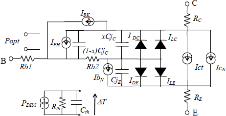
Except for optical parameters, the rest of this model refers to a HBT model.
Th electrical currents are modeled by two ideal diodes currents:
with:
−βf and βr being direct and reverse current gains respectively;
−nE and nC are diode ideality factors;
−Isf and Isr are saturation currents.
The currents of the two non-ideal diodes are:
with C2 and C4 being balance coefficients for saturation currents.
Current ICT is given by:
[4.37] ![]()
Expression of junction capacitances is given by the general expression:
where:
−V is junction voltage;
−Cj0 is capacitance for zero voltage;
−φ is junction barrier potential;
−m is junction profile dependent coefficient.
The base collector capacitance is separated into two parts: xCjC and (1-x)CjC as a function of the geometry and disposition of the optical window. RC, RE, Rb1, Rb2 are the access resistances.
Current IBK is an empirical expression simulating the base-collector junction breakdown. It must not be too abrupt so not to introduce numerical instability in the calculation:
Bf, Rbr, CM, Nbr are empirical parameters fitting with characteristics IC = f (VCE).
The procedure to obtain these parameters for a particular transistor is detailed in [POL 04].
Thermal effects are accounted for due to a particular circuit (Figure 4.34) where the current source is:
A thermal resistance Rth and capacitance Cth account for substrate thermal resistance and capacitance. For example, in an InP/InGaAs transistor, Rth = 2,000 K/W and Cth is modified so the thermal time constant (RthCth) is equal to 2 µs. Transistor temperature is now given by:
and a new current is defined by equation [4.42], in which ICT(T0) is defined by equation [4.37]:
[4.42] ![]()
where XT is modified by approximating the measured continuous current from the transistor.
The optical parameters are modeled by equation [4.32].
The noise response is obtained by associating each resistance of the diagram with a voltage source on a band of 1 Hz, corresponding to thermal noise:
In the base and collector, noise current sources IbN and IcN are given by shot noise relations linked to currents IDE and ICT:
These steps are detailed in [POL 04] and in this reference it is possible to find several sets of values for a particular phototransistor.
The simulations with this model in a circuit simulator give S-parameters of the phototransistor used in the following section.
4.3.7. Influence of the base load impedance
The input of a phototransistor is optical. The output is an electrical signal on the collector and it is also possible to load (or add a signal) on the base port. The phototransistor, configured as a common emitter, is hence considered a tri-port whose gain between optical input and collector output depends on the base load. Since the first realization of phototransistors, researchers have had the intuition that this load is important [KAM 95b] but the first complete assessment of the problem was only carried out by [POL 99]. This same work was also presented in [THU 99] and evoked in [HOU 06]. The complete process was detailed in [RUM 03] and [POL 04].
Small signal behavior of a phototransistor can be demonstrated as in Figure 4.35.
Figure 4.35. Small signal phototransistor: S parameters
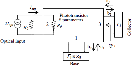
As will be presented in the following chapter, the optical input is represented by the current detected by a perfect photodetector. Optical input is on port 2. Load R0 represents that optically, for the moment, input reflection is not accounted for. The base is represented by port 1. Collector output is on port 3. The reflection coefficient Г3 represents the possibility of a perfect matching at the output. Reflection coefficient Г1 represents the load possibilities that can be introduced to the base.
To make clear there is perfect isolation between electrical and optical signals, the following definitions are introduced: S22 = S23 = S12 = 0.
With these definitions, the optomicrowave gain between optical input and collector port can be written [POL 99]:
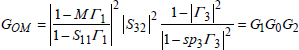
with:
and:
![]()
If the output is matched: Г3 = sp3 * and the gain becomes:
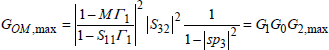
What is remarkable in these expressions is that the base load (Г1) only affects gain G1. On a Smith chart it is possible to plot the gain GOM,max as a function of Г1 or as a function of ZB, for a particular transistor at a fixed frequency. This is the transistor from Figure 4.24 with a gradual base and for a frequency of 32 GHz. It is shown in Figure 4.36.
Figure 4.36. Phototransistor optomicrowave gain as a function of all the possible impedances presented to the base port. The positive real parts of impedance are inside the Smith chart, and the negative real parts are outside
The figure shows the minimum (point marked “zero”) and the maximum (cross marked “pole”) of GOM,max both appear for negative real parts of the load impedance ZB, in other words outside the Smith chart. The maximum gain with a positive real part is obtained on the chart contour (point marked “maximum”), in other words the impedance will be purely reactive. It is similar for the minimum gain.
To research maximum and minimum gains of such a phototransistor, a circuit presenting the base with all possible reactive impedances (contour of Smith chart) is required. This is proposed in [SCH 09] where a microwave cable of 1 m-length is connected to the transistor base port. The end of this cable is closed on either a short circuit, an open circuit, or on a resistance of 50 Ω. If the cable end is closed on a short circuit or an open circuit, when the microwave signal carried by the optical wave is frequency scanned, the base port is loaded by all the possible reactive impedances. When a resistance of 50 Ω is used to close the input, the base is always loaded by this impedance.
In reality, the impedances are not purely reactive at high frequency due to cable losses. The results towards 1 GHz show an improvement of 10 dB in the gain between the case of maximum gain and the case where an impedance of 50 Ω is presented. The results are particularly interesting for circuit design using phototransistors.
4.3.8. Summary
AlGaAs/GaAs or GaInP/GaAs phototransistors operate for a wavelength of 0.85 µm, thus limiting their use.
InP/InGaAs phototransistors operate up to optical wavelengths of 1.55 µm. Their optical cutoff frequency can be very high (300 GHz) but at the price of having to use specific technology.
Si/SiGe operate at optical wavelengths of 0.85 µm and can also function with an optical wavelength of 1.1 µm. However, their responsivity is relatively low. Phototransistors operate with technologies compatible with classical Si/SiGe HBT technologies, allowing them to be combined with diverse microwave circuits such as amplifiers, mixers, and oscillators.
For all phototransistors, studies have shown their performances can be improved by optimizing the base load.
Amongst the techniques developed to improve responsivity, insertion in an optical cavity thanks to Bragg reflectors is very promising.
4.4. Appendix
4.4.1. Lattice matched layers pseudomorphic layer, metamorphic layer
4.4.1.1. Lattice matching
Semiconductor materials used for microwave photonic components are crystalline. When several layers must be superimposed (lasers, photodiodes, phototransistors), a rule to remember is that the different layers grown one over the other (epitaxied) must have identical lattice constants. For this, it is useful to look at Figure 4.37.
In this figure different materials are described:
– simple elements. Crystals such as Si or Ge correspond to points in Figure 4.37;
– III-V binary compounds: covalent bonds. These materials are composed of elements from groups III and V from the periodic table. These materials have a single possible proportion of the two materials (GaAs, InP). They correspond to a single lattice constant and single gap value in Figure 4.37;
– IV-IV binary compounds. The valence orbitals of these elements are electronically saturated, they can be constituted of different proportions of each component. For example, SiGe corresponds to a line linking lattice constants to bandgap values in Figure 4.37;
– III-V ternary compounds. These III-V compounds comprise two elements of group III or two elements of group V with varying proportions. These compounds (InGaAs) correspond to a line in Figure 4.37. To make a material grow over another, certain proportions must be respected to achieve identical lattice constants. For example, all proportions of AlxGa1-xAs where all the x values correspond to the lattice constants of GaAs or InGaAs of which a single proportion (In0.53Ga0.47P) corresponds to the lattice constant of InP. AlInAs is identical;
– III-V quaternary components. These III-V compounds (InGaAsP) are composed of two elements of group III and two elements of group V with varying proportions. Numerous combinations are possible and there is no unique representation. It is hence possible to independently adjust the lattice constant and bandgap.
An example can be given for the InxGa1-xAsyP1-y compound. It is possible to continuously vary the bandgap of this compound from the value of In0.53Ga0.47As (ΔE = 0 eV) up to that of InP (ΔE = 0.6 eV) all the while conserving the lattice constant, which is identical for In0.53Ga0.47P and InP (see Figure 4.37). For this, y must be varied while respecting the constraint [CAM 82]:
Figure 4.37. Bandgap and lattice constants for different compound semiconductors
4.4.1.2. Pseudomorphic layer
Even if the lattices do not completely match, it is always possible to grow a layer with a lattice constant slightly different to the first crystal layer. As long as the lattice match difference is small (below 1%) and as long as the thickness is small, the layer is stable. It is thus possible to epitaxy a SiGe layer on Si to make a bipolar transistor base (very fine layer). As long as the proportion of Ge is not too big, the SiGe layer constraint thus obtained is stable (see Figure 4.37).
4.4.1.3. Metamorphic layer
In the case of very large lattice constant disagreement, another technique was employed. It consists of completing a transition layer that assures a bond between two layers with very different lattice constants.
Figure 4.38 gives an example of such a layer. To understand this figure, it must be recalled (Figure 4.37) that, regardless of the proportions of Ga and Al, AlGaAs bonds with GaAs and that Al0.48In0.52As bonds withIn0.47Ga0.53As. This arrangement allows p-i-n photodiode creation with InGaAs on a GaAs substrate and hence joins these diodes with AlGaAs/GaAs HEMT devices [HUR 97].
Figure 4.38. Metamorphic layer
4.4.2. Velocity overshoot effect
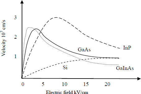
Figure 4.39 represents electron velocities in different materials as a function of an established electrical field. These curves are hence obtained in static conditions.
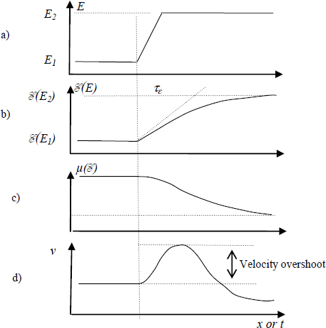
If the electric field is very rapidly altered or if the electron moves in a region where the electric field changes over a small distance, these are dynamic conditions and the electron velocity varies in a different manner. This new velocity variation is represented in Figure 4.40.
Figure 4.39. Static velocities in different semiconductors
The curve in Figure 4.40a represents what is produced for an electron moving in a material such as GaAs. The electric field changes from a stationary value, E1 (e.g. 4 kV/cm), to a stationary value, E2 (e.g. 20 kV/cm), over a short distance or time. The curve in Figure 4.40b shows that under the electric field effect, the electron acquires an increasing energy but this energy variation is no longer instantaneous (relaxation time of energy τε).
The curve in Figure 4.40c shows the variation of electron mobility as a function of the decrease in acquired energy. Finally the curve in Figure 4.40d is the electron velocity obtained by expression v = μE. This curve shows a velocity overshoot two or three times larger than the maximum velocity of curve 4.40d. In GaAs, this phenomenon appears for electric field variations over lengths of 0.5 µm [CAS 89].
Figure 4.40. Dynamic electrons: velocity overshoot
4.4.3. Heterojunction bipolar phototransistor
Phototransistors are based on a HBT structure in which there is a window to allow light through. It is hence important to remember the configuration of such a transistor as well as its equivalent circuit diagram and the principal relations allowing the calculations of fT and fmax frequencies of this transistor. These aspects are taken from [RUM 04b] in which there is a succinct presentation of these transistors. Similarly, [SCA 09] provides a presentation of all high-frequency transistors and explains the position of HBTs in relation to other transistor types.
Microwave bipolar transistors are all n-p-n types and all have an emitter-base heterojunction. In this transistor, the emitter-base heterojunction has an emitter composed of a large bandgap semiconductor and a base composed of a small gap semiconductor. The semiconductors must be chosen so that the bandgap difference is on the valence band side. This results in blocking the holes that could come from the base towards the emitter and, thus, increases the emitter injection efficiency. Thus, the base can be doped more than that of a homojunction bipolar transistor base and its thickness can be reduced, leading to an increase in the transistor operational speed, without increasing the transistor base resistance RB. The configuration of an example HBT is shown in Figure 4.41. This description is taken from [DEL 94].
Figure 4.41. Configuration of a double mesa self-aligned GaInP/GaAsHBT
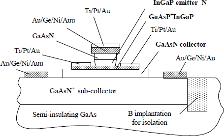
Figure 4.42 illustrates the stacking of the materials and the corresponding doping for an intrinsic transistor. This stacking must be done with semiconductors of identical lattice constants. For this, the InGaP is actually In0.48Ga0.52P. In these transistors, the emitter is aligned on the base due to a dry etching, which must stop exactly at base level. InGaP has the advantage of facilitating the differential etching and thus increasing transistor reliability.
This structure serves as a base to numerical simulation of this transistor when it is used as the phototransistor in [CHE 99].
Figure 4.42. Materials and doping level for the intrinsic transistor in Figure 4.41
If this transistor is put in a common emitter configuration and biased to a fixed biasing point, it is possible to evaluate the linear or small signal response of the transistor by making measurements of microwave S parameters and to extract a more or less complex linear equivalent circuit. An example of such a model is given in Figure 4.43 where a pi-equivalent circuit is represented.
From this model, it is possible to calculate the different transistor gains (for transistor biasing and small signal gains, see [RUM 04b]):
- the current gain for short circuit output: Gi;
- transducer power gain GT when the transistor is loaded to 50 Ω at the input and output. It is the gain obtained during S parameter measurements, i.e.:
![]()
- the maximum available gain Gmax (or MAG). This gain is obtained by presenting a complex conjugate of admittances to the transistor input and output. This is the same as saying that the inputs and outputs are perfectly matched. Under these conditions, numerous transistors become unstable in some frequency ranges, and so, Gmax does not exist in this range;
- the Mason gain is then required, which consists of calculating the maximum gain of a transistor that has been previously unilateralized, in other words, the counter reaction (introduced by CBC) is compensated for by a parallel pure inductance. It is for this reason the gain is also called unilateralized gain, GU.
Figure 4.43. Pi-small signal equivalent circuit for a HBT
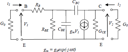
The above gains are represented in Figure 4.44. The curves of this figure are obtained from the following values: RB = 20 Ω; RBE = 24.6 Ω; CBE = 2.9 pF; CBC = 9 fF; GCE = 4 mS; g0 = 785 mS; τ = 1.75 ps; G0 = 1/50 = 20 mS. On these curves two frequencies appear corresponding to gains equal to 1 (0 dB).
Figure 4.44. Different gains of the diagram of Figure 4.43
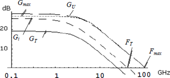
In one part the frequency for which the current gain Gi is equal to 1, is frequency fT or the transistor frequency of transition given by the equation:
Elsewhere the frequency, for which maximum or unilateralized gain is equal to 0 dB, is frequency fmax. In principle it is the maximum frequency for which it is possible to realize an oscillator with this transistor type. This second frequency is very important in microwaves as it is linked to the maximum gain possible for a simultaneous input and output matching. An approximate expression is:
With these model values it is also possible to determine the approximate minimum noise factor of such a transistor. It is given by expression [FUK 66]:
[4.51] 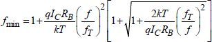
with IC in milliamps and q/kT = 0.04/V for T = 293 K.