Chapter 2
Generation and Modulation of Light
2.1. Laser
2.1.1. General points
In microwave photonic links, the first component to consider is the optical source, which is now always a laser diode.
The history of laser invention is complex and eventful. Although some facts are still disputed [AGR 86; BER 99; TAY 00], the main milestones of this invention can be sketched:
– the first stimulated emission demonstration appears to have been carried out in 1947 by W. E. Lamb and R. C. Retherford [BER 99], and in 1950, A. Kastler proposed an optical pumping method, demonstrated by Brossel, Kastler, and Winter in 1952;
– in 1953, C. H. Townes and his research students, P. Gorgond and H. J. Zeiger, created the first pulsed MASER (Microwave Amplification by Stimulated Emission of Radiation). Independently, N. Basov and A. Prokhorov (USSR) created a CW MASER; Townes, Basov, and Prokhorov got the Nobel Prize in 1964;
– in 1957, A. L. Schalow and C. H. Townes published the principles of an optical MASER;
– the term “laser” (light amplification by stimulated emission of radiation) was introduced in 1959 by G. Gould, who filed a patent the same year. This patent was only recognized by the American patent office after 18 years of proceedings. The authorization to receive royalties on this patent, and the others, required another 10 years of proceedings [TAY 00];
– the first pulsed solid-state laser (a 694 nm emitted wavelength ruby crystal pumped by a flashlamp) was created in 1960 by T. H. Maiman;
– later that year, A. Javan and his collaborators, W. R. Bennett and D. Herriot, created the first helium-neon gas laser;
– the semiconductor laser diode was proposed in 1962 by N. Basov and A. Javan, and was realized in the infrared region of the optical spectrum by R. N. Hall and in the visible region by N. Holonyak Jr. This type of laser requires biased currents of 50 kA/cm2 forcing it to operate in the pulse mode;
– in 1970, Z. Alferov and, separately, I. Hayashi and M. Panish developed a CW semiconductor laser diode by using heterojunctions to enable the reduction of the biased current by a factor of 100;
– multiple quantum well structures appeared in 1979. The first realized one used successive layers of gallium arsenide (GaAs) and aluminum gallium arsenide (AlGaAs) delivering a power in the order of 50 mW. These lasers emitted in a spectral window of 0.8 to 0.9 µm, which corresponds to an attenuation that is too high for an optical fiber. It is for this reason that telecommunications research directed itself towards indium gallium arsenide phosphate (InGaAsP) composites, in order to emit wavelengths in the order of 1.3 or 1.5 µm.
In direct modulation systems, the optical source is a semiconductor laser diode. In external modulation systems, the optical source was initially a solid-state laser, such as Nd:YAG; however, semiconductor lasers are slowly replacing them due to their low cost, compactness, their great flexibility, and increased performance [BET 97]. Further, it is during direct modulation, always performed with a semiconductor laser, that laser performance is more likely to influence link performance. As a consequence, in this section, only semiconductor lasers will be studied.
Their structure and performance have evolved considerably, but it is possible to explain their operation in relation to a number of configurations and to present models demonstrating the resultant effect on link performance. In effect, a microwave photonic link only uses the optical wave as a support, which should only slightly disturb the transmission; however, actually, as will be shown in Chapters 5 and 6, it is the noise, distortion, and possibly the deterioration of spectral purity of the microwave signal by the laser that principally contributes to link performance.
2.1.2. Semiconductor laser structure and optical gain in the active zone
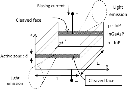
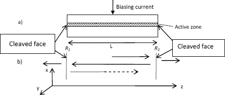
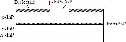
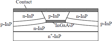
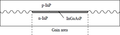
Figure 2.1 presents a simplified diagram of a double heterojunction semiconductor laser. Stacked layers of indium phosphide (InP)-doped p — intrinsic InGaAsP — InP-doped n constitute a p-i-n diode. The application of a bias current to this diode induces a carrier population inversion in the thin (d = 0.15 µm) GaInAsP layer, which stimulates the emission of photons. The two cleaved surfaces in the active zone constitute incomplete reflective mirrors forming a resonant optical cavity that produces the wavelength. These surfaces allow one or several spectral lines of light, to escape making this device an optical source. In addition to its thickness, d, the active zone has a length, L, and width, l, of ~300 µm and ~150 µm, respectively.
Figure 2.1. Semiconductor laser configuration
The operation of a semiconductor laser is detailed in several works. The present description is based on [AGR 86; AGR 92; EBE 93; HIN 93]. The p-i-n laser junction of Figure 2.1 is forward biased above the threshold current, a current passes directly across this junction, and electrons of the active zone are carried to a higher energy level situated in the conduction band. At the same time, holes appear in the valence band of this semiconductor. This operation constitutes an electron population inversion in connection with the zero bias state semiconductor. In this zone, photons can produce several phenomena.
An electron can spontaneously combine itself with a hole. As a result a spontaneous photon emission occurs. This emission is the origin of noise in the laser, but it is also required to start the laser, which is an oscillator.
If its energy is sufficient, the spontaneously emitted photon can be absorbed by the semiconductor by generating an electron-hole pair. This phenomenon is used in photodetectors.
The photon can trigger the combination of a conduction band electron with a valence band hole; this causes the emission of one or many photons in phase with the previous emitted photon. This coherent photon emission is stimulated emission.
Figure 2.2. GaAs optical gain in terms of incident photon energy
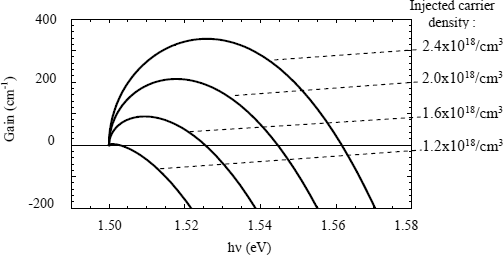
Therefore, it is possible to calculate the optical gain (number of photons emitted per unit length for an incident photon) of a semiconductor in terms of the injected carrier density and, consequently, of the applied current. For this the equations and calculation methods are presented in [ROS 98] and a calculation example is given for GaAs. The results are shown in Figures 2.2 and 2.3. Figure 2.2 represents the optical gain in terms of incident photon energy and injected carrier density and Figure 2.3 shows the maximum gain of Figure 2.2 in terms of carrier density and, therefore, applied current. The curve is practically straight. The maximum gain occurs with a reduction in wavelength in terms of carrier densities of approximately 1 nm per 1017/cm3
Figure 2.3. Optical gain maximums in terms of GaAs injection carrier density
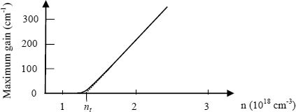
According to Figure 2.3, the relation between gain and carrier density, n, can be expressed as follows:
[2.1] ![]()
where:
nt is a transparency carrier density per cm3;
a is a differential gain coefficient in cm2.
2.1.3. Operation of a Fabry-Perot laser
Figure 2.4a represents the laser in Figure 2.1 longitudinally. Figure 2.4b represents the photon trajectory in the active layer from spontaneous emission.
Each reflection coefficient at the extremities of the active zone is given by:
where nr is the refractive index of the semiconductor.
The refractive index is also susceptible to change if anti-reflective added layers are deposited upon the cleaved laser surfaces.
Figure 2.4. a) Fabry-Perot laser diagram and b) photon trajectory
The photons are represented by a plane wave with an electric field of amplitude E0, a frequency, v, and a propagation constant k = 2πvnr /c (where nr is the material’s refractive index) and the active layer presents a power gain, g, and a power absorption loss, aint. After one round trip in the laser cavity, the field gain is exp[(g/2)(2L)] and the field loss is (R1R2)1/2 exp(-2Lαint/2).
If only considered after a round trip between the two cleaved faces, the electric field amplitude should not have changed and it is possible to write:
This translates into a condition on intensity and phase:
[2.4] ![]()
[2.5] ![]()
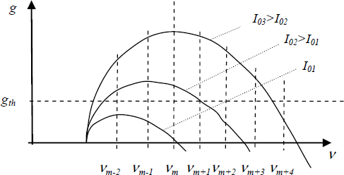
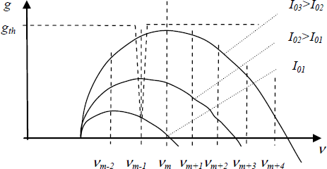
In [2.4], gth corresponds to the maximum gain (or threshold) of the semiconductor so oscillation can begin and the term on the right corresponds to losses in the cavity αcav (internal losses αint and losses due to mirrors αmir) or the inverse of photon lifetime τp multiplied by vg.
Regarding equation [2.5] corresponding to laser modes, it fixes optical frequencies νm for which an oscillation can be produced. A complete relation should take into account the variance of nr with frequency.
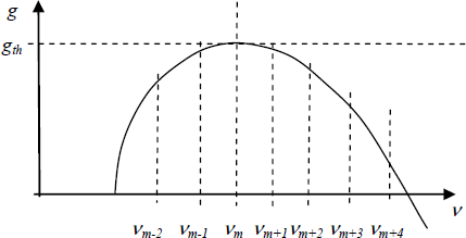
For the oscillation to take place at a single frequency, it is possible to adjust the gain (injected current) as shown in Figure 2.5. Fabry-Perot lasers simultaneously produce several modes. Changes in laser structure (DFB laser, Bragg mirror lasers) allow the development of single-mode lasers.
Figure 2.5. Gains in the active zone in terms of optical frequency: different possible laser modes
2.1.4. Optical confinement factor and rate equations
Optical wave energy is not entirely confined to the active zone. Figure 2.1 represents a vertically oriented laser section showing an active zone comprising a semiconductor (GaInAsP) with a smaller bandgap than the two surrounding layers (InP).
This corresponds to a slightly higher refractive index and, thus, to optical wave confinement.
Figure 2.6. Vertically oriented optical confinement factor computation
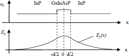
In reality, as represented in Figure 2.6, the Ey component of the electric field spreads out the active zone and the optical confinement factor is defined by:
where the variables are recalled in Figure 2.6: the x-axis is oriented vertically and the transverse electric field, Ey, is in the lateral direction.
There is also a lateral optical confinement factor, Γl, (y-axis horizontal orientation in Figure 2.1) which is dependant upon the presence or absence of a laterally oriented semiconductor, for example, in buried structures (Figure 2.14). Of course, this depends upon the configuration of the laser. The overall confinement factor can be expressed as:
It is now possible to describe the rate equations of a one-dimensional laser (in term of length), but where the confinement factor gives a lateral first approximation. These rate expressions are:
[2.8] ![]()
[2.9] ![]()
In these expressions:
– N and P are the carriers and photons numbers in the active zone;
– NT is the number of carriers on the transparency threshold: NT = nt / V;
– I is the biasing current;
– q is electron charge;
– τn and τp are the carrier and photon lifetimes;
– vg is the velocity of the optical wave group in the active zone, also expressed as vg=c/ng where ng is a group index;
– β, the spontaneous emission coefficient, is very weak as only the spontaneous photons are considered, the wavelength of which correspond to that of the laser;
– V is the volume in the active zone.
Also found in these expressions is the maximum gain coefficient, a, from expression [2.1].
Expression [2.8] is the carrier conservation equation. The first term corresponds to generation process due to induced current. The second term corresponds to the carrier recombination in the absence of stimulated emission (non-radiative recombination and spontaneous radiation). The third term corresponds to the recombination processes due to stimulated emission.
Expression [2.9] describes the photon conservation equation. The first term corresponds to photon generation due to stimulated emission, as the second term is due to spontaneous emission. The third term corresponds to photon loss within the cavity due to the optical absorption (see equation [2.4]).
2.1.5. Static mode of laser operation (or CW mode of operation)
In the CW (continuous wave) mode of operation, electrons or photons are considered time-independent so:
![]()
and if spontaneous emission is considered negligible, equation [2.9] allows:
implying:
– either P = 0, no photon emission;
– or, above the threshold, the electron density, N, which is constant and equal to N0, calculated at threshold, is then given by:
[2.11] ![]()
Below the threshold (P = 0), by using equation [2.8]:
Above the threshold, by using equation [2.8] and [2.11]:
[2.13] ![]()
where I0 is the static current fixed above the stimulated emission threshold.
From this expression, the threshold current is deduced at P = 0:
[2.14] ![]()
So equation [2.13] can be written:
[2.15] ![]()
The emitted optical power is proportional to P0 due to the current I0.
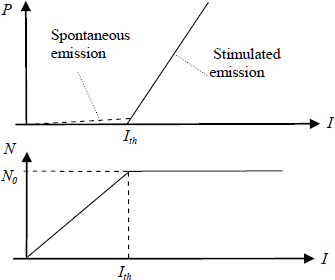
Figure 2.7 represents the curves of the photon and electron density variations in terms of biasing current I.
In this figure the dotted line represents the spontaneous emission contribution below the threshold, which has been disregarded in the above equations.
The power POPT emitted by one of the two faces of the laser can be written:
[2.16] ![]()
where the ½ coefficient corresponds to the case R1 =R2.
Figure 2.7. Diagram of a static laser response where N=electron density and P=photon density
2.1.6. Dynamic mode of laser operation: RF small signal response
When a RF small signal is superimposed on the DC biased laser current, which is the case for all applications evoked in this work, the dynamic response of a laser can be evaluated. According to the approximations made, the results differ from one publication to another. The expressions below focus upon the steps presented in [EBE 93] but introducing the Г coefficient in each continuity equations as in [2.8] and [2.9] to evaluate the small signal response, the magnitudes I, P, and N are replaced by:
[2.17] 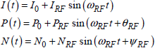
where:
I0, P0, N0 are static values already used above;
IRF, PRF, NRF are the microwave small signal magnitudes for one mode;
θRF, ψRF are the small signal phases of P and N.
The values of [2.17] are inputs in equations [2.8] and [2.9], allowing the extraction of the number of supplementary carriers and photons in terms of time. After a Fourier transform, their frequency terms are extracted, providing Pm in terms of ωRF (or fRF):
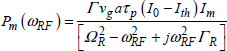
with:
![]()
and:
![]()
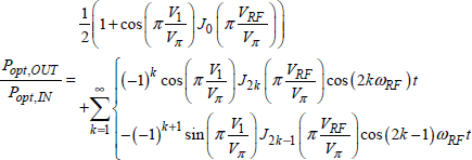
The relative modulus value of PRF (ωRF) over PRF (0), defined for the static mode of operation, is given by:
[2.19] 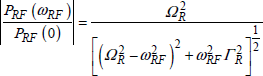
The parameter values of a given laser are listed in Table 2.1 [BIB 98]: its threshold current is equal to 20 mA (equation [2.14]). Figure 2.8 shows the relative small signal responses of photon numbers in terms of the induced signal (equation [2.19]) for several laser-biased currents I0.
Table 2.1. DFB laser parameters [BIB 98]
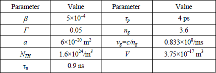
Figure 2.8. Relative small signal response from laser in Table 2.1 in terms of RF frequency and for several biasing currents
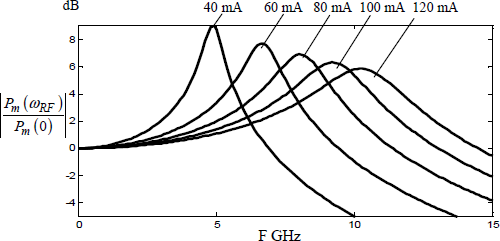
As can be seen in Figure 2.8, an increase in the biasing current corresponds to a maximum frequency shift on the dynamic response, and therefore, an increase in the relaxation oscillation frequency ΩR. At the same time the damping coefficient ГR increases. This curve gives only a trend because, as shall be seen later, a decrease in microwave frequency must be added to the laser response due to the biasing circuit of the laser.
2.1.7. RIN laser noise
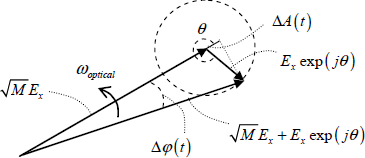
In this case a continuously biased laser is considered which emits a continuous wave and noise. The noise is principally due to spontaneous emission. The spontaneous laser emission phenomena have been described in Chapter 1. The spontaneous emitted photons produce incoherent light, even those emitted during stimulated emission. The fraction of these photons corresponding to the fluctuation of the laser wavelength is characterized in a Fresnel diagram as in Figure 2.9.
Figure 2.9 shows the combination of a spontaneously emitted photon electric field with M coherent stimulated emission photons. The combination of vectors corresponding to these two emissions can be characterized by intensity ΔA(t) and phase ![]() fluctuations. However, in an “intensity modulated (IM) direct detection (DD)” link, only the intensity modulation remains after detection. Laser phase fluctuations will therefore not be considered here.
fluctuations. However, in an “intensity modulated (IM) direct detection (DD)” link, only the intensity modulation remains after detection. Laser phase fluctuations will therefore not be considered here.
Figure 2.9. Fresnel diagram showing the coherent M photon and spontaneous photon electric field
Laser intensity and phase noises have been comprehensively described in [YAM 83a; YAM 83b]. For a simplified presentation, the description in [EBE 93] will be recalled again. The step consists of adding elements called Langevin forces to equations [2.8] and [2.9], becoming:
[2.20] ![]()
[2.21] ![]()
where FN (t) and FP(t) are the Langevin forces corresponding to random signals defined by a Gaussian process (〈 FN (t)〉 = 〈FP(t)〉 = 0) of which the auto-correlation functions in the simplified approach of [EBE 93] correspond to:
[2.22] 
where δ(Δt) is a Dirac function.
After the insertion of equation [2.22] into equations [2.20] and [2.21], the physical expressions are transformed into frequency dependent expressions and the spectral densities of Langevin forces are written:
where fRF is the microwave frequency and ΔfRF is the microwave band magnitude.
The noise power intensity spectrum can be expressed as:
From the last expression and taking into account equations [2.11], [2.14], and [2.15], it is possible to define relative intensity noise or RIN:
[2.25] 
This expression has dimensions related to the square of two optical powers multiplied by ΔfRF. This expression accounts for the fact that after photodetection the ΔfRF term disappears and hence the ratio of two electrical powers is obtained. For ΔfRF = 1 Hz, the value of equation [2.26] (in decibels per hertz) can be expressed by: RIN dB/Hz=10 log(RIN).
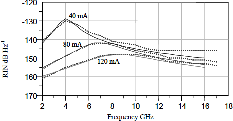
Figure 2.10. RIN in decibels per hertz for the laser of Table 2.1
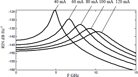
By considering the laser parameters described in Table 2.1, Figure 2.10 gives an example of RIN values in decibels per hertz in terms of frequency.
For ω << ΩR, the RIN value varies from −148 to −143 db/Hz with I0 varying from 40 to 120 mA.
When the laser biasing current increases, the RIN diminishes, and its frequency response follows the small signal dynamic response of the laser.
2.1.8. Increase in 1/f of RIN and superposition of a small signal and noise
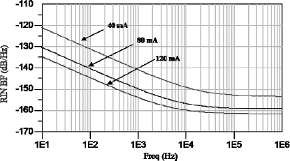
In Figure 2.10 the RIN seems to become constant, whereas the electric signal frequency tends to 0 in agreement with equation [2.25]. In reality, this noise increases in 1/f at very low frequency. Although not explained, this noise, which is very common in nature and inherent in all optoelectronic components, cannot be omitted. This noise has been studied in [DAU 94] with a laser of identical characteristics as that of Table 2.1. This noise has the appearance given in Figure 2.11 in terms of frequency and for several biasing currents [BDE 06]. Similar to RIN, it decreases with an increase of the biasing current.
Figure 2.11. 1/f RIN for the laser of Table 2.1
The superposition of the small signal response described in section 2.1.6 on RIN described in section 2.1.7 is obtained in principle by linearly adding the corresponding signals. However, as shall be seen later, the laser response is nonlinear. Although direct detection is supposed to eliminate phase fluctuations, in reality, an optical heterodyning between small signal microwaves and 1/f noise (such as those in Figure 2.11) deteriorates the spectral purity of a microwave signal transmitted by direct laser modulation.
In section 6.2, the formulation of this phenomenon is described and the consequences for the transmission of a RF signal modulating an optical wave are evoked.
2.1.9. Different laser configurations
2.1.9.1. Gain- or index-guided configurations
One type of laser is the lateral emission or edge-emitting laser (EEL) [CAB 03b]. For this kind of laser, Figures 2.1 and 2.6 evoke the vertically oriented optical wave confinement. To achieve a good lateral confinement several configurations are available.
The first method is to perform guidance by the gain. This possibility is described in Figure 2.12. The carriers are injected into a particular zone of the semiconductor, thus limiting the area where a photon gain occurs.
Figure 2.12. Gain-guided laser structure
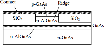
The second and third methods are carried out by refractive index guidance. Figure 2.13 shows a ridge-type structure. The InP was etched in order to form a ridge around which a deposit of SiO2 is laid. The difference in refractive index between SiO2 and p-InP is of the order of 0.01. The laser mode is thus laterally guided around the ridge; however, the guidance is weak.
Figure 2.13. Ridge-type laser structure
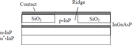
Figure 2.14 represents a buried structure, in which, the heterojunction is totally surrounded by materials with different refraction indices ranging from 0.2 to 0.3. This corresponds to a strong index guidance. These types of structures are called buried-heterostructures (BH).
Figure 2.14. Buried-type laser structure or “buried-heterostructures” (BH)
2.1.9.2. Fabry-Perot lasers
The laser described in Figure 2.1 is a Fabry-Perot laser. The cleaved faces determine the modes that can appear in the longitudinal direction. The reflection coefficients and losses of the cleaved faces within the material determine the gain threshold value (equation [2.4]). However, the biasing current in the heterojunction determines the carrier density and, therefore, the photon gain (Figure 2.2). The combination of equation [2.4] and Figure 2.2 gives Figures 2.5 or 2.15.
In this figure it seems that for a given gain threshold, the number of possible modes and, especially the corresponding maximum of frequency displacement, increase with induced current. The Fabry-Perot laser is hence defined as a multimode and, therefore, multifrequency laser.
In reality, due to an antagonistic pumping effect on the principal mode, the number of modes tends to decrease with biasing current increase [VAP 90, p. 144]. The fact remains that Fabry-Perot lasers are multimode lasers and are not suitable for the majority of optical links. This is why other configurations have been proposed.
Figure 2.15. Growth of mode numbers in a Fabry-Perot laser in terms of biasing current
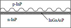
2.1.9.3. Distributed feedback laser (DFB) or distributed Bragg reflector laser (DBR)
One solution to avoid the generation of several modes is to configure the laser in such a manner that the gth (corresponding to a loss) line behaves as in Figure 2.16. In this case, a single mode is selected whatever the laser biasing current.
Figure 2.16. Curve showing gain threshold in a single-mode laser
This result can be obtained by using the diagram structure in Figure 2.17. The diagram shows a selective optical feedback at a single frequency depending on the Bragg reflector period. This type of laser is often used in optical links [CAB 03a].
Figure 2.17. Diagram of a DFB laser
Another solution is to place Bragg reflectors at the active zone extremities as shown in Figure 2.18. In this structure the reflectors exhibit total reflection except at a particular frequency, thus producing a single-mode laser.
Figure 2.18. DBR laser diagram
One of the two Bragg reflectors in Figure 2.18 can be replaced by a cleaved face from which coherent laser light is emitted.
2.1.9.4. Single-layer or quantum well active regions
The first semiconductor lasers were created on a GaAs substrate, the active layer was also GaAs, sandwiched between two layers of AlGaAs to ensure good optical confinement by index guidance. All the above configurations of lasers (DFB or DBR) were first created with this material, as represented in Figure 2.19 for a ridge laser. The emitted wavelength from these lasers is 0.85 µm.
As shown in the introduction this wavelength corresponds to a fiber attenuation that is too high to create links tens or hundreds of kilometers long. As a result InP substrate lasers were developed with multi-layers semiconductor processing described in Figures 2.12, 2.13, 2.14, and 2.18. These lasers allow emissions of 1.3 or 1.5 µm wavelengths according to the composition of the quaternary compound, InGaAsP.
Figure 2.19. GaAs active layer ridge laser diagram
Microwave photonic links can be appropriate for short distances for which the fiber attenuation is no longer a limiting factor. For this reason GaAs substrate lasers are once again being used both in EELs and vertical cavity surface-emitting lasers (VCSEL), as will be shown.
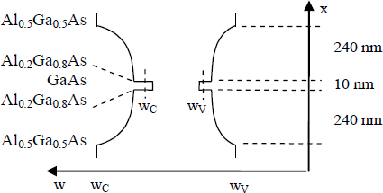
Concerning the active layer, another proposed solution consisted of a structure composed of one or several quantum wells. The first realizations included a GaAs well surrounded by AlxGa1-xAs layers, with x varying from 0.2 to 0.5 with increasing distance from the quantum wells. This solution introduces a gradual refractive index variation and hence good quantum confinement. Figure 2.20 [EBE 93] represents such a structure called Graded Index Separate Confinement Heterostructure or GRINSCH.
In this figure the thickness of the GaAs layer leads to a quantum well. The energy gaps are determined by the difference between wC and wV. In GaAs, this gap depends upon the well size. This type of laser therefore emits wavelengths slightly above 0.85 µm.
Figure 2.20. GaAs quantum well laser structure
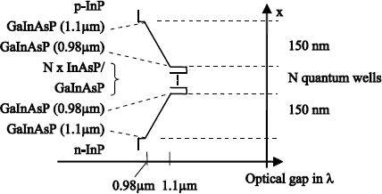
Structures producing lasers emitting wavelengths of 1.3 or 1.5 µm were proposed in [PAN 99; TSA 84]. Figure 2.21 shows such a structure for a laser emitting a wavelength of 1.3 µm [CHU 98].
Figure 2.21. InP quantum well laser structure
Lasers with this type of structure show a higher differential photon gain and a weaker threshold current, especially when the number of quantum wells is low (1 or 2). The counterpart is that the active zone is small and the emitted power is low (a few milliwatts). These structures have no advantages over easily implemented VCSEL lasers, described below.
2.1.9.5. VCSEL laser
The previous sections only considered EELs. A very different structure was proposed introducing a vertical cavity. The light emission then occurs perpendicularly to the semiconductor surface: these are vertical cavity surface-emission lasers or VCSELs. This type of device has given rise to considerable development activity, which is still ongoing. A summary of these devices are found in [IGA 00] and [RIS 03].
Three phases can be considered for the development of these devices: the first idea and the initial demonstration were proposed in 1977; the first realization took place in 1988 [IGA 00]; and 1999 marked the beginning of 0.85 µm and, thereafter, 1.3 µm wavelength laser production. Currently, a number of studies are being undertaken to improve 1.3 µm lasers and to begin production of 1.55 µm lasers.
Figure 2.22. Vertical cavity self-emitting laser (VCSEL)
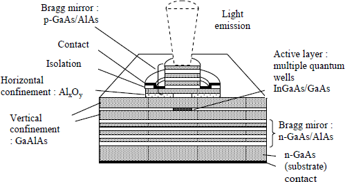
The diagram in Figure 2.22 shows the configuration of a 0.85 µm VCSEL laser. This type of laser can, therefore, be considered to be similar to a DBR laser shown as such in section 2.1.9.3, but with an emission perpendicular to the surface. The different layers of the Bragg reflectors serve to vary the refractive index while maintaining a good crystalline lattice match without the gap value causing absorption. For this, GaAs/AlAs structures are suitable for a number of wavelengths from 0.8 to 1.6 µm. The lower mirror is composed of approximately 30 layers of GaAs/AlAs, whereas the upper mirror is composed of 17.5. However, the active layer must emit light and the corresponding materials are compatible in lattice constant with AlGaAs only for 0.85 to 0.9 µm wavelengths (GaInAs low in In). This active layer is realized in the form of multiple quantum wells, as mentioned in the previous section. An example of an active layer consists of three 8 nm GaInAs quantum wells and two 8 nm GaAs quantum well barriers, sandwiched between two 120 nm GaAlAs vertical confinement barriers. Horizontal confinement is realized by part oxidation of aluminum in the GaAlAs layer.
With the same structure, a 1.3 µm emitting laser can be obtained using high In-content GaInAs quantum wells in the active zone. Thus, the crystalline lattice no longer matches and the quantum wells are created by constrained layers. It is thereby possible to have an indium content of up to 40% (1.3 µm emission), but no more.
The characteristics of VCSELs can be better appreciated when compared against EELs as shown in Table 2.2 [IGA 00].
Table 2.2. Lateral or vertical emission laser comparison
| Parameter | EEL | VCSEL |
| Active layer height (nm) | 10-100 | 8-500 |
| Active layer surface area (µm2) | 3 × 300 | 5 × 5 |
| Active layer volume (µm3) | 60 | 0.07 |
| Cavity length (µm) | 300 | ~1 |
| Mirror reflection | 0.3 | 0.99-0.999 |
| Optical confinement (%) | ~3% | ~4% |
| Lateral optical confinement (%) | 3-5% | 50-80% |
| Vertical optical confinement (%) | 50% | 2 × 1% × 3 (quantum wells) |
The advantages of the VCSEL structure are also listed in [IGA 00]:
– the small volume of the active layer corresponds to a small threshold current. For example, by using the above expressions it is possible to get: (I0/Ith-1)>100;
– the wavelength and the threshold current are relatively insensitive to temperature;
– it is possible to have a single transverse optical mode;
– the relaxation frequency is high, allowing a high modulation frequency;
– the buried active layer results in increase of its lifetime (in an EEL structure, the reliability defects due to surface area effects are very important for non-buried structures);
– high optical conversion rate (see Table 2.2);
– vertical emission: can facilitate optical coupling;
– whether they have several transverse modes or a single mode, such as the more recent VCSELs, the wide emitting surface leads to a thinner beam that is more easily coupled to an optical fiber;
– the manufacturing process is monolithic, leading to low costs or the possibility of integration with other digital or analog monolithic structures;
– preliminary tests can be automatically performed, over a probe station, directly upon a semiconductor wafer before chip cutting;
– the possibility of making bidimensional laser networks to increase power.
The main VCSEL disadvantages are:
– the low volume active layer gives an optical emission performance which is always limited in power (0.1 to a few milliwatts);
– in transverse orientation, the optical cavity is relatively large, allowing several simultaneous transverse optical modes. The first VCSELs were thus multimode lasers. The most recent VCSEL have become, once again, single-mode lasers by emphasizing lateral optical confinement. For this, Figure 2.22 shows an optical lateral confinement gain structure due to the disposition of the upper electrode. However, this device also comprises a refractive index for optical confinement due to the oxidation of Al in an AlGaAs layer. The AlxOy obtained has a lower refractive index than the semiconductor, causing a lens effect that concentrates the electric field to the center of the laser;
– for wavelengths above 1.3 µm, the active layer (for example, the GaInAsP in quantum wells) must be surrounded by InP, producing very unstable and complex technological structures (see [OHI 01] and [OHI 02] for examples) that are not readily fabricated.
It has been noted that for short links, lasers emitting at 0.85 and 1.3 µm can be very useful and surface-emitting lasers are currently being used.
2.1.10. CAD laser models
2.1.10.1. Static and dynamic laser models
The laser model described below can be used in circuit simulation software in the frequency domain and for linear and nonlinear analysis. This is a large signal model. It builds upon continuity equations as implemented in sections 2.1.3, 2.1.4, and 2.1.5. The variable definitions are the same and the product N.P, introduces the nonlinearity to the model. So to simulate the output optical power saturation effects observed on measurement, a phenomenological coefficient, ε, reinforces the nonlinearity. The modified continuity equations are:
[2.26] ![]()
[2.27] ![]()
These expressions can be rewritten introducing a photon density s = ΓP /V and an electron density n = N /V:
[2.28] ![]()
[2.29] ![]()
To simulate these expressions in a circuit simulation software, an equivalence between photon density, s, and a software variable, for example, the voltage, Vs, must be found. Photon density being proportional to optical power, this choice allows a linear expression between the input current and the output optical power. From a numerical point the ill-conditioned equations [2.28] and [2.29] must also be considered because the relation between values n and s are of the order 1020. These conditioning and equivalence are realized by multiplying photon density by a variable Sn.
This leads to:
with Sn=2×1024 V-1.m-3.
In this expression, the variable s is a photon density, but in an electrical simulator, this photon density is represented by an equivalent voltage Vs.
Now, equations [2.28] and [2.29] can be written as:
[2.31] ![]()
[2.32] ![]()
These expressions show a biasing laser current, I, a spontaneous current, Isp, and a stimulated current, Ist. These currents can comprise a static and a dynamic part (see equation [2.17]). Thus, equations linking voltage VS to current by an equivalent electrical scheme are obtained, allowing the introduction of equivalent resistance, RP, and capacitance CP. The definition of these magnitudes are:
The time derivatives can be directly simulated or, if the biasing current is sinusoidal, it can be written:
With these definitions, equations [2.31] and [2.32] become:
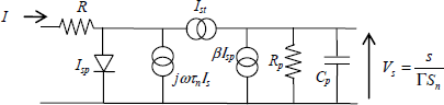
This equation system can be solved by circuit simulation software, such h as ADS, by introducing Figure 2.23. In this model the current source can be break it up in a DC and an AC parts as in equation [2.17].
Figure 2.23. Laser electrical equivalent circuit model for circuit simulation software
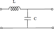
This intrinsic model is generally completed by parasitic elements (extrinsic model) placed at the input, which model the connections as a low w pass filter, these elements are extracted from microwave measurements on n the laser. An example of such a circuit is given in Figure 2.24.
Figure 2.24. Example of parasitic elements at laser entry
The optical power at the laser output is expressed slightly differently than in expression [2.16], because one of the two mirrors is now completely reflective:
where:
η is an external quantum efficiency (ratio between generated and injected photons);
ν is the optical frequency;
h is Planck’s constant in joules.
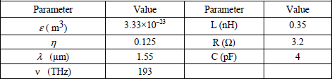
A simulation example created under ADS software was undertaken using the laser parameters given in Table 2.1 and completed by parameter values and parasitic elements of Table 2.3 [BDE 06]
Table 2.3. Parameters and parasitic elements for the stimulated laser
Stimulated laser dynamic response in intensity is shown in Figure 2.25.
Figure 2.25. Simulation of a laser dynamic response in amplitude for several continuous biasing currents
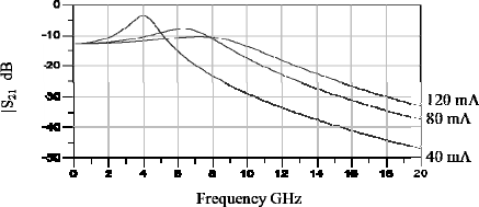
In Figure 2.25, the S21 parameter is an optomicrowave S-parameter corresponding to the definitions given in Chapter 5. The expression for this parameter is:
where:
R0 is a microwave matching resistance (generally 50 Ω);
Im is the intensity of the biased alternating current.
Compared with the results obtained in Figure 2.8, which does not correspond to |S21|2 but to the PRF (ωRF) / PRF (0) ratio, it appears that reduction of the resonance frequency is linked to the introduction of the connection equivalent circuit.
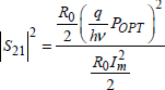
In this equation, the ![]() expression corresponds to a current detected by a perfect photodetector. This current can therefore be complex and the S21 parameter has a phase represented in Figure 2.26.
expression corresponds to a current detected by a perfect photodetector. This current can therefore be complex and the S21 parameter has a phase represented in Figure 2.26.
Figure 2.26. Simulation of the dynamic response phase of a laser for several continuous biasing currents
The model of the laser represented in Figures 2.23 and 2.24 also gives static and large signal laser responses. This allows formulation and characterization of second and third-order laser nonlinearities. The characterizations of nonlinearities for a complete link will be given in Chapters 5 and 8.
2.1.10.2. Noise models
As seen in section 2.1.7, the laser RIN is modeled by the introduction of two Langevin sources in the laser continuity equations. Equations [2.26] and [2.27] then become:
These time-dependent expressions are then transformed to frequency-dependent expressions and frequency Langevin forces appear, which are introduced in the equivalent laser equivalent circuit as sources of noise current. The expressions given in section 2.1.7 for these Langevin forces were simplified. The expression giving the Langevin forces and so the model noise sources are now a little more complete [BDE 06]:
It is thus possible to deduce a new equivalent model (Figure 2.27), with two additional noise current sources (random white and Gaussian signal) defined by the equations above. From this model, it is also possible to simulate the RIN response versus RF frequency with ADS software; the results of which are shown in Figures 2.25 and 2.26. The result of RIN simulation is shown in Figure 2.28 where it is compared with noise measurements performed on the same laser type.
Figure 2.27. Laser intrinsic model including current sources to represent RIN
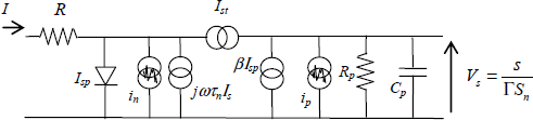
Figure 2.28. Laser RIN simulation and comparison with measurements (dotted line) for several biasing current values
These curves are similar to those obtained by an approximate expression presented in Figure 2.10.
2.1.11. Laser measurements and temperature stabilization
The above described laser models do not yet describe the behavior of all the devices. Numerous characteristics must be obtained by measurements. For example, the intensity noise measurements (see Figure 2.25) or phase noise measurements as a result of microwave modulation. These measurements give rise to complex activities outside the scope of this work.
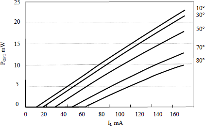
For example, one of these measurements is presented in Figure 2.29 [ALO 09]. The lasers are very sensitive to temperature and this figure shows the static response of a DFB laser in terms of ambient temperature. The optical power emitted by the laser decreases when the temperature increases; subsequently, the threshold current increases with temperature. Finally, the optical power nonlinearity in terms of biasing current also increases with temperature.
Figure 2.29. DFB optical power measurements as a function of temperature [ALO 09]
The variation of threshold current with temperature can be described by a simplified expression [AGR 92]:
In this expression, I0, depends upon the configuration and dimensions of the laser, value T0 is above 120 K for GaAs lasers and 50-70 K for InGaAsP lasers.
The very large laser sensitivity to temperature means that a number of them are equipped with a temperature stabilization system as is schematized in Figure 2.30 [TEL 06]. The temperature regulation of lasers has given rise to an abundance of studies in the literature [ERS 06: SEM 06].
Figure 2.30. Laser cooling system
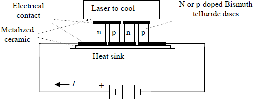
The cooling is based upon the Peltier effect. When a DC current I circulates in the Bismuth telluride discs arranged as in Figure 2.30 (electrical series setup), the heat is transferred from the laser towards the heat sink (thermal parallel setup). Current I is controlled by a microprocessor or a simple amplifier connected to a biasing transistor that able to produce a continuous optical current-to-power ratio output (e.g. the curve relative to a temperature of 20°C can be deduced from Figure 2.29). The measurement of the optical current is performed by a very simple photodiode closely positioned to the laser.
2.2. Electro-optic modulator: EOM
The modulation of an optical signal by a lower frequency signal (analog or digital) can be directly performed a laser diode applying an AC biasing current, or via an intermediate external modulator at the output of the diode.
The latter solution has a number of advantages: a higher applied power modulated RF signal and a signal higher frequency, reaching the millimeter-wave spectrum [BAR 04; MEN 88; TSU 03].
External modulation technology of an optical signal is based on three different physical principles: electro-optic effect, electro-absorption effect, and gain modulation effect with light injection. Only the first two effects will be discussed in this chapter.
The birefringence, or double refraction, of a material is its capacitance to present a variable refractive index in terms of the application of an external force, i.e. an electric field, a magnetic field, or a mechanical constraint. The refractive index depends on propagation direction and light polarization, causing an ordinary and extraordinary refractive indices: induced isotropic birefringence and altered anisotropic birefringence can occur.
Electro-optical modulation occurs while a material is under an electric field causing variation in the refractive index, which affects the propagated optical signal. Two physical effects can cause this birefringence: (1) the first-order electro-optic effect or Pockels effect, whereby the birefringence is directly proportional to the electric field, and (2) the second-order (quadratic) electro-optic effect or Kerr effect where the birefringence is proportional to the square of the electric field [CAR; HUI 89].
2.2.1. General physical principles
A material under an electric field ![]() shows a polarization
shows a polarization ![]() which can be expressed in the form of a limited expansion:
which can be expressed in the form of a limited expansion:
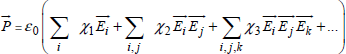
ε0 is the permittivity of free space, Ei is the components of all the electric fields present in the crystal and χn is the n order dielectric susceptibility tensor relative to the materials. The linear response of the environment is characterized by χ1: wave refraction and reflection. The higher-order terms are nonlinear and become influential if the intensity of the electric field is large. Term χ2 particularly indicates the interactions between two fields in the environment: electro-optical Eopt. Eelect (Pockels effect) or optical-optical E2opt (mixing function and generation of harmonic frequencies). Term χ3 indicates the Kerr effect among others, due to the term Eopt. E2elect [HUI 89].
2.2.2. Pockels or linear electro-optical effect
The Pockels effect appears only in crystals with no center of symmetry, like KDP (potassium dihydrogen phosphate), ADP (ammonium dihydrogen phosphate), lithium niobate (LiNbO3), InP, and GaAs.
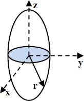
A crystal is represented by the index ellipsoid in a three-dimensional space (x,y,z) corresponding to its principle dielectric axes, on the surface of which the trajectory r gives the solutions of n:
For an isotropic material, the three indices are equal to n0 and the ellipsoid becomes a sphere.
Generally, when an electric field is applied, the index ellipsoid is modified and can be deformed:
[2.49] ![]()
By developing equation [2.49], and using a linear approximation, an electro-optic tensor is obtained (equation [2.50]), which expresses the refractive index difference in terms of electric field. The tensor coefficients are very low (a few tens of pm/V) and some are considered to be zero; therefore, their values are different depending on the crystal: the electrooptic effect occurs if the applied electric field is high (in the order of 107 V/m). This electro-optic effect depends on the orientation of the electric field and on the light polarization compared with crystal cross-section. Thus, in a crystal for which the coefficient r13 is the strongest, the electric field must be applied on the z axis, the light propagates along the y axis with a linear polarization on the x axis; the index change will be induced along the x axis:
[2.50] 
Table 2.4. Crystal or electro-optic material parameters
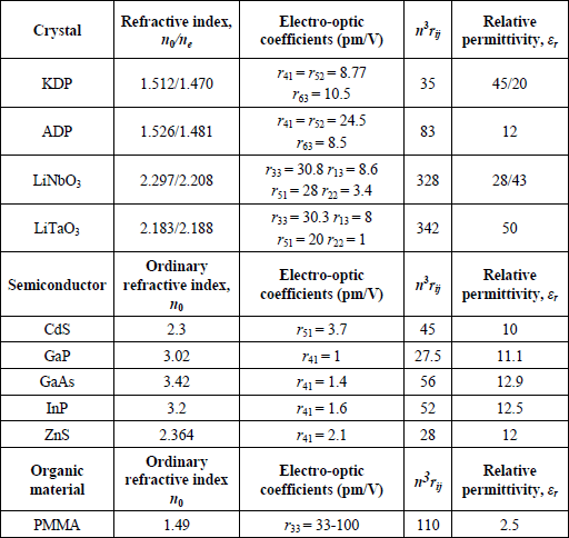
Table 2.4 lists the linear electro-optic coefficient values and the physical parameters of frequently used crystals.
Amongst these materials, LiNbO3 has the strongest electro-optic coefficient and, therefore, the Pockels effect dominates [CAR]. In anisotropic materials the refractive index depends on the propagation direction; they are the most frequently used to fabricate Mach-Zehnder electro-optic modulators. For a longitudinal configuration, only phase modulation is introduced. For a transverse configuration, a phase and intensity modulation is introduced. This latter configuration is the most often used.
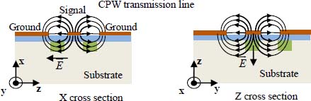
According to the crystal axis direction, an x-cut section modulator for which the electric field is horizontal and the optical wave TM mode is used, is distinguished from a z-cut section modulator, for which the electric field is vertical and TE mode is used (see Figure 2.33). Thus, for these two cutting orientations, the higher tensor coefficient r33 must be considered.
It must be noted that the cut-off RF frequencies are higher for the z than for the x-cut sections, thus the modulation is nearly doubled and able to achieve speeds of over 40 Gb/s [GOU 04].
For the z-cut crystals, the index variation is written according to equation [2.51] by considering the low index variation. The quadratic coefficient, s33, is negligible for LiNbO3, it introduces compression phenomena at high voltages, allowing dynamic range evaluation [HUI 89]:
[2.51] ![]()
2.2.3. Mach-Zehnder electro-optic modulator
This modulator exploits the Pockels effect. It is presented as an optical wave guide, which separates the optical wave into two branches due to a Y-junction. On each branch, a different applied electric field, introduces a phase difference.
The connection at the output of the two branches, with the help of a second Y link, allows the combination of the two mutually interfering output waves (Figure 2.32).
Figure 2.32. Mach-Zehnder E/O modulator and its cross-section
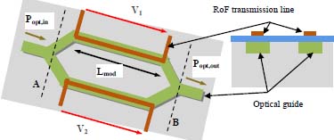
The applied electric field at a very high frequency allows the modulation of an optical signal up to 40 Gb/s [BAR 04; DOL 92; GOU 04]. LiNbO3 modulators are able to achieve frequencies of 100 GHz [NOG 98]. The electric field is applied through a planar transmission line, which via coupling in the optical guide, creates an electrical field in the crystal. The transmission line dimensions must be optimized to minimize the effect of the mismatching phenomena on the applied microwave signals. The planar transmission line can be created via two different technologies: microstrip or coplanar waveguides [GUP 96]. The latter technology is the most often used for Mach-Zehnder modulators as their electrodes are single-sided. Hence, they have a ground plane on the upper substrate face unlike microstrip technology.
For naturally anisotropic LiNbO3, the field can be applied to x or z-cut sections according to the line position on the waveguide as shown in Figure 2.33. The representation of the electromagnetic field that propagates along the transmission line indicates the orientation of E in the optical waveguide. According to these two configurations, the crystal is oriented in such a manner that the optical axis is parallel to the electric field.
Figure 2.33. Mach-Zehnder EO modulator on LiNbO3: x and z-cut sections
The operating principle of the modulator is based upon a phase difference or an optical delay between each of the two optical signals. The length of the modulator branch Lmod is large enough for an optimal RF and optical wave coupling, which is typically 2 cm for a LiNbO3 modulator.
2.2.4. Single-Drive MZM: one driving electrode
If a RF signal is applied on one electrode and the second remains grounded, the phase of each optical signal arising in B is written:
The phase difference between the two optical waves is then expressed linearly in terms of applied voltage on branch 1; the sign depends on the orientation of the electric field compared with the optical field:
where β0 represents the propagation constant, or phase constant, of the optical wave which is constant in vacuum, Lmod the length of the RF modulation line, VRF1 is the RF voltage applied on branch 1 of the modulator, d is the distance between the two electrodes, Γ is the recovery coefficient between the optical and electric fields in the crystal [RAM 82], n0 is the refractive index in the waveguide:
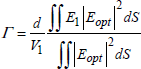
Coefficient Γ is between 0 and 1 [GOU 04] and dS represents an element of the waveguide section.
Vπ is the voltage applied to the modulator to obtain a phase difference of π; it represents an intrinsic characteristic of the material for the whole wavelength:
From this, the variation of optical field propagating between the input and output of the modulator can be determined, and then deduce the optical power.
At the electro-optic modulator input (Figure 2.32), at point A, the optical field is written:
This field is uniformly divided in each optical branch, in such a manner that at the modulator output (point B), the field is equal to the sum of two optical fields that have travelled the Lmod distance of each optical branch, introducing a phase difference linked to the variation of the biased branch refractive index:
The optical wave electric field at the modulator exit is calculated by considering that each Y junction divides the optical power by 2 in the optical guide. Indeed, the optical mode coupling is equals to 50% at each junction.
This field can also be expressed in the following manner:
[2.58] 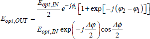
Hence, the optical field shows phase and intensity variations induced by the applied voltage on electrode 1, which correspond to an amplitude and phase modulation of the optical signal:
[2.59] ![]()
The optical power deduced from Poynting theorem is written:
[2.60] ![]()
or expressed in terms of the voltage applied on an electrode:
[2.61] ![]()
2.2.4.1 Static mode of operation
Figure 2.34. Optical field and power at modulator output in terms of continuous voltage V1
If a DC continuous voltage is applied on branch 1, equation [2.61] indicates the power from the modulator will vary sinusoidally between 0 and Popt, IN, as in the plots in Figure 2.34. Optical power varies in terms of voltage V1, extinction appears for a voltage equals to Vπ, corresponding to two waves of opposite phase cancelling in plane B (Figure 2.32). The power is a maximum when no biasing occurs, and is halved for Vπ/2. Around this biasing voltage the optical power variation is linear, allowing an optical signal modulation by complex data, providing the modulation intensity stays linear.
This is only true for a totally symmetric modulator. An asymmetry always exists between the two modulator branches, generating a residual phase difference between the two biasing free optical signals, corresponding to a voltage offset inherent to the modulator [GOU 04]:
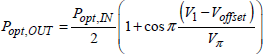
Figure 2.36 represents the power at the modulator output in terms of time for a wavelength of 1,550 nm. The optical signal weakening is observed as V1 approaches Vπ.
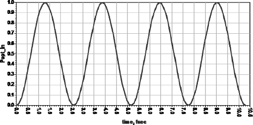
Figure 2.36. Optical power at 1,500 nm modulator output where V1 varies from 0 to Vπ, (decreasing curves)
2.2.4.2. Dynamic mode of operation
2.2.4.2.1. One-tone RF signal is applied
If sinusoidal and continuous biasing voltages are superimposed upon each other, the optical wave electric field has its amplitude and phase modulated by the applied electrical signal (equation [2.64]). The output optical power is thus amplitude modulated (equation [2.64]). A photo-receiver detects the optical power and generates a current proportional to the power contained in the modulated signal:
[2.64] ![]()
The electric field intensity can be developed in a series of Bessel functions corresponding to the sum of the intermodulation products between the optical frequency and the RF signal harmonics, products whose level is a function of the applied continuous electrical and sinusoidal voltages on the electrode (equation [2.65]). Hence the RF signal once again finds itself transferred as a double sideband around the optical carrier:
[2.65] 
The Jn functions represent first kind of n-order Bessel function. The analysis of these results shows that the spectrum is strongly dependent on the biasing voltage and RF signal amplitude. If it is considered that the RF voltage is weak in amplitude, i.e. VRF << Vπ, then first kind of n-order Bessel function are written:
[2.66] 
Г(n + 1) is the Euler function, which is equal to n ! when n is an integer.
In low amplitude RF signal approximation, these functions are respectively written for the first terms, and neglecting k-order terms greater than 1 (equation [2.66]) for each Bessel function:
[2.67] 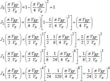
The appearance of the spectrum at the modulator output can be determined in terms of the applied continuous and RF voltages by using equation [2.65]:
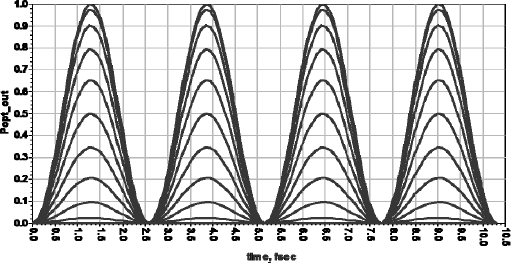
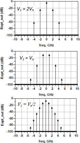
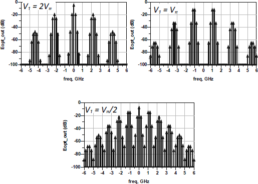
– by basing the electrode at 2Vπ or 0, only the even components appear around the optical carrier, the intensity of each component diminishing when the order increases;
– by biasing at Vπ, only the odd components appear and the optical carrier cancels;
– by biasing at Vπ/2, all the components appear around the optical carrier.
These results correspond to the simulations represented in Figure 2.37.
Figure 2.37. Optical spectrum at modulator output if an RF signal (1GHz) is applied to one electrode, as a function of the biasing voltage V1
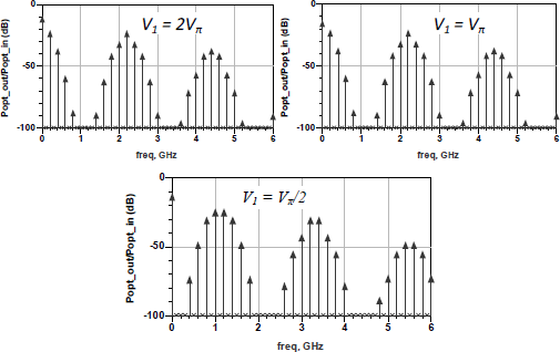
2.2.4.2.2. Two-tones RF signal applied
If two sinusoidal RF signals are applied to electrode 1, the development of an electric field, considering only the main lines, becomes:
[2.68] 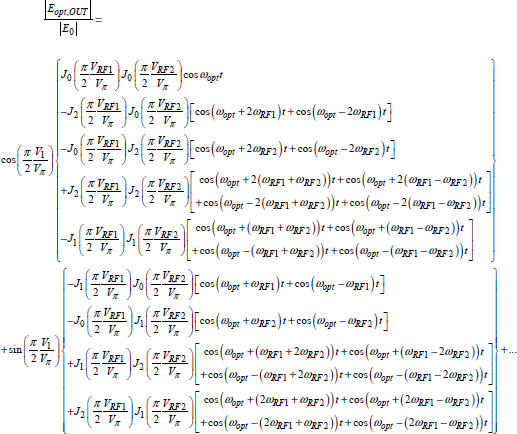
The following figures show the simulation results on the optical spectrum at the exit.
The influence of the biasing voltage corresponding to the analysis of one-tone applied RF signal, as described above, is observed, but the decreasing of the intensity of the products is also noticed.
These simulation results can be deduced from equation [2.69], which corresponds to a simplified equation [2.68] by replacing the Bessel functions by their simplified expansion (equation [2.67]).
The amplitude of each component is directly proportional to a VRF term elevated to a power of n:
[2.69] 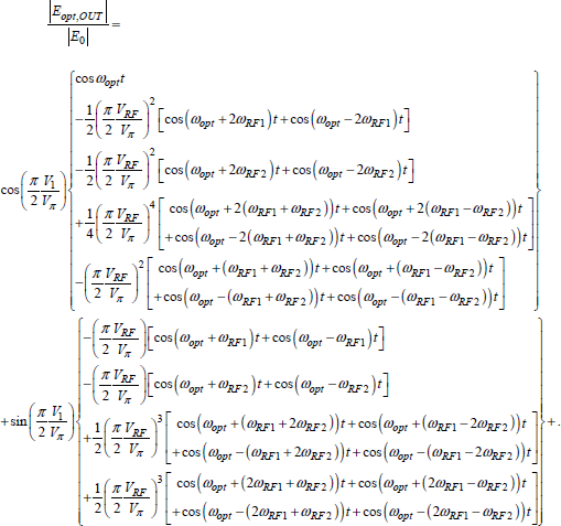
The influence of voltage allows the cancelling of the optical carrier r and/or to highlight certain harmonics. The spectrums of Figures 2.37 and 2.38 represent the optical carrier (centered at 0) modulated by intermodulation products between RF signals.
This simulation was performed using a commercial software package (ADS) for microwave circuits by using an envelope method and a nonlinear r component, which models the electro-optic effect of a modulator. As the RF frequencies are far from the optical frequency, a classical physical or harmonic balance method cannot be used [ADS].
Figure 2.38. Optical spectrum at modulator output if two-tones RF sign as (1 and 1.2 GHz) is applied to one electrode, as a function of the biasing voltage V1.
2.2.4.2.3 Optical intensity and power
The demodulation of an optical signal, in frequency or phase, requires a coherent optical receiver, which is complex to produce and has low performance because it requires a mixer, a local oscillator, and an optical filter [COX 04; SEE 96]. However, its sensitivity is better than that produced using direct detection. Nevertheless, the sensitivity with direct detection can be greatly improved by using an optical amplifier.
Considering only the case of direct detection and detecting only the optical wave intensity, all information concerning optical carrier phase and frequency is hence discarded. This intensity, I, is directly proportional to the optical power, as shown in equation [2.70], and therefore, to the square of the amplitude of the electric field:
[2.70] ![]()
Thus the spectrum can be represented in optical power. However, as the detection is quadratic, it is different from the field spectrum and contains a larger number of intermodulation products. The desired signal envelope is uniquely obtained: the optical carrier disappears and only the signal envelope is obtained. In the same way, only the detectable single sideband RF signals are examined.
By considering the low modulation indices, i.e. a low-amplitude modulating RF signal, it is possible to neglect many of the intermodulation products and to consider the optical spectrum close to the field spectrum.
For example, where a single RF signal is applied at a biasing voltage of Vπ/2, the optical power is simply written as an amplitude modulation of the index modulation equal to πVRF/Vπ, by considering the limited expansion of the first-order sine function:
[2.71] ![]()
A smaller expansion provides the expression of the optical power as a function of one or two applied RF signals. Thus, from equation [2.64], an additional DC term appears in relation to the electric field expansion, as well as different intermodulation products. The optical carrier disappears as only the signal envelope is required:
In the case of low modulation and a biasing index at Vπ/2, by considering terms from J3 as negligible (equation [2.67]), the latter being proportional to the amplitude VRF cubed, equation [2.71] is found.
By expanding the first terms while two RF signals are applied, the optical power is the sum of the even intermodulation products multiplied by cos(πV1/Vπ) (equation [2.73]), and the odd intermodulation products multiplied by sin(πV1/Vπ) (equation [2.74]):
[2.73] 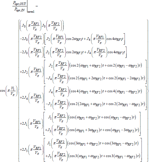
[2.74] 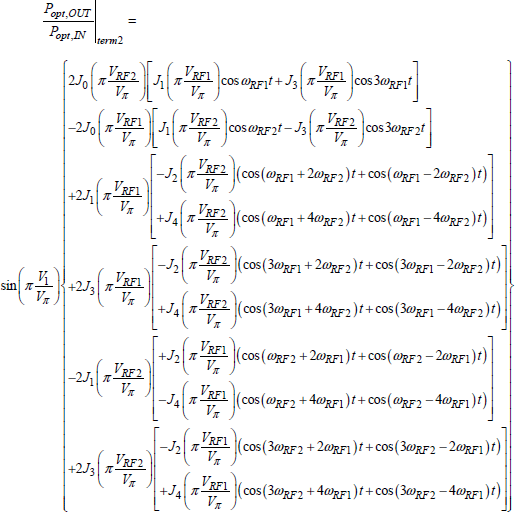
Figures 2.39 and 2.40 represent the intensity simulated spectrum in the same simulation conditions as those represented for the field (Figures 2.37 and 2.38).
The spectrums found in this case are different from those found with field equations. Only the signal envelope is considered. While two RF signals are applied the principal intermodulation terms calculated from equation [2.74] are found. Nevertheless, for low modulation indices, many intermodulation products can be neglected and the field and power spectrums are close. Only the power spectrum is considered because only direct detection is taken into account.
Figure 2.39. Intensity at modulator output if one-tone RF signal (1 GHz) is applied on one electrode, as a function of biasing voltage V1
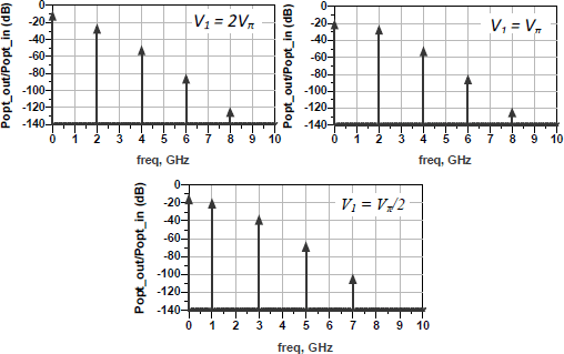
Figure 2.40. Intensity spectrum at modulator output if two-tones of RF signal (1 and 1.2 GHz) are applied on one electrode, as a function of biasing voltage V1
2.2.5. Dual-drive MZM: two driving electrodes
In this configuration each modulator electrode is biased. The z-cut section is the most appropriate for this. From structure symmetry, it is considered that the two recovery coefficients between the fields are identical.
In this case the optical signal phase introduced by each branch is written:
The phase difference becomes:
The modulator voltage, V’π, is hence expressed:
The expressions of electric field at the modulator output as well as optical power are given by equations [2.58] and [2.60].
2.2.5.1. Static mode of operation
The application of two equal continuous voltages of equal absolute values such as V1 = -V2 corresponds to a working identical to a single-drive MZM, as a function of V1.
2.2.5.2. Dynamic mode of operation
The interest is in the application of two different signals on each of the electrodes.
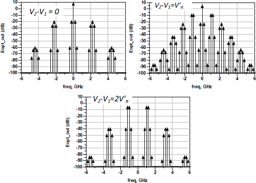
The series expansion of Bessel functions leads to an infinite number of terms of which the following are predominant:
The optical carrier is double sideband modulated. The variation of biasing voltages allows the interesting frequencies to be highlighted. The following figures give the envelope simulation results using ADS software for different DC biasing voltages.
Single-drive modulator similar results are recovered:
– by applying a biasing with no difference between the two electrodes, only the even components appear around the optical carrier;
– by applying a biasing difference between the two electrodes of 2V’π, only the odd components appear and the optical carrier is cancelled;
– by applying a biasing difference between the two electrodes of V’π, all the components appear around the optical carrier.
Figure 2.41. Optical signal at modulator output if a different RF signal is applied on each electrode: fRF1 = 1 GHz and fRF2 = 1.2 GHz
More complex signals can also be introduced as a binary sequence: the digital signal is found around the RF signal frequency, but also around the optical carrier, and even the resulting intermodulation products are seen.
2.2.6. Real Mach-Zehnder modulator: characteristics and performances
The description of the previous function essentially rests upon the electro-optic effect and its influence upon the optical signal. Strictly speaking, the modeling of this component type cannot occur without an electric and microwave model, which inevitably induces maximum modulator frequencies and the accompanying losses. These losses can be taken into account by introducing an attenuation coefficient on the field or optical power (equations [2.59] and [2.60]). This coefficient takes into account both the optical losses in the guide and the fiber coupling losses.
The coupling between the two electrical and optical electric fields is executed along the entire electrode length; however, the two waves do not propagate at the same speed across the modulator. The optical wave travels the length Lmod with a velocity of c/n, n corresponds to the crystal refractive index equals to ![]() , whereas the RF signal travels at a velocity equal to
, whereas the RF signal travels at a velocity equal to ![]() , εreff corresponds to the relative effective permittivity of the transmission line [GUP 96]. While the optical wave propagates in a homogenous environment, the RF signal electromagnetic field propagates in two environments: the crystal and the air above. At the modulator output, the two waves propagate at different velocities, inducing a phase shift. On the contrary, if the two waves propagate at similar velocities, the phase difference becomes small, and the coupling-enabled RF signal frequency becomes very large. This harmony between propagation velocities is realized by using progressive wave modulators (TW-MZM) [KUB 80; GEE 83] and by optimizing electrode dimensions in such a manner as to minimize the mismatching and reflection phenomena of the RF wave.
, εreff corresponds to the relative effective permittivity of the transmission line [GUP 96]. While the optical wave propagates in a homogenous environment, the RF signal electromagnetic field propagates in two environments: the crystal and the air above. At the modulator output, the two waves propagate at different velocities, inducing a phase shift. On the contrary, if the two waves propagate at similar velocities, the phase difference becomes small, and the coupling-enabled RF signal frequency becomes very large. This harmony between propagation velocities is realized by using progressive wave modulators (TW-MZM) [KUB 80; GEE 83] and by optimizing electrode dimensions in such a manner as to minimize the mismatching and reflection phenomena of the RF wave.
The main characteristics of a Mach-Zehnder modulator are:
– maximum operating frequency: resulting from the phase difference between optical and RF waves:
– modulation depth: in the case of amplitude modulation, I represents optical intensity at biasing voltage V:
– optical extinction rate:
– optical bandwidth at 3 dB: modulation depth divided by 2;
– electrical bandwidth: modulation depth divided by ![]() ;
;
– insertion losses:
– figure of merit: allows modulator comparisons [WAL 91]:
where Z is the modulator impedance, feo the electro-optic band magnitude, Vd the command voltage, and λ the optical wavelength;
– chirp: corresponds to the change of carrier frequency (optical wave) during the modulation.
The transmission line associated with the electrode, through the technology used and its dimensions, corresponds to a lowpass filter and is associated with a characteristic impedance. Modeling can be carried out by electromagnetic simulations and the results can be integrated into the electric simulation software to calculate its influence upon the signals. Thus we can visualize eye patterns, calculate Binary Error Rates and the Error Vector Magnitude in high speed optical communications, simulate the dynamic range, the chirp, and the known component defects. This was realized for the electro-absorption modulator, and is applicable to all well-known components as shall be shown in the following sections [DES 07a; DES 07b; DES 09, ALG 10].
2.2.7. Mach-Zehnder modulator technology
This technology was discussed in section 2.2.2, during the description of the principle electro-optic materials. Four materials are mainly used for the production of this component: LiNbO3, polymers, GaAs, and InP.
The first material undoubtedly performs best in terms of optical losses (0.2 dB/km), working frequencies [MEN 88], and strong Pockels effect, but the biasing voltages are higher (4-7 V) due to the high value of Vπ. Currently, it is the most studied and most used [WOO 00]. Frequencies of 110 GHz associated with bandwidths of 70 GHz have been attained [NOG 98]. The modulation length is 1-2 cm and the total losses vary from 3-7 dB. Nevertheless a modulator has been reported to operate at a voltage of 1 V [SUG 02].
InP is very interesting as its dimensions are smaller (a few millimeters in length), as are its operational voltages (1-3 V) and it can be integrated into OEMIC circuit technology operating at 1,550 nm. Operational frequencies of 40 GHz have been attained [BAR 04; MEN 88; TSU 03]. However, the optical losses are higher in an InGaAsP guide: 1 dB/km, which is compensated for by smaller lengths.
GaAs has also been thoroughly studied and has shown performances of up to 40 GHz [HAX 03; SPI 95]. Circuit production technology using GaAs is well established. This substrate use is interesting in terms of cost and the control of the physical characteristics of the layers. Furthermore, the substrate wafers are available in 6" diameters, whereas InP or LiNbO3 are only available in 3" and 4" diameters.
Polymers, such as polymethyl methacrylate (PMMA), are interesting because not only do they have the highest electro-optic coefficients (in the order of 90 pm/V for PMMA-DR1) [LAB 02; LEE 02], but also the lowest insertion losses at millimeter frequencies, a low command voltage, simple and cost-effective production technology. Furthermore, the square root of the effective relative permittivity is very close to the refractive index, facilitating electrode dimension optimization to equal the two optical and RF wave propagation velocities [ALG 05; DAL 03]. The electro-optic effect is associated with the doping of PMMA with chromophoric molecules [LEE 00]. Thus frequency performances of up to 110 GHz have been reported for a PMMA modulator [CHE 97]. The losses can range from 6-10 dB.
Devices have also been fabricated using silicon substrates and based on silicon-germanium/silicon (SiGe/Si) heterostructures [HEM 89; TRE 91; ZHA 95], in order to develop a low-cost technology compatible with circuits integrated on silicon.
This technology has the disadvantages of a small optical confinement, large dimensions, and a limited bandwidth, linked to low RC value [LI 99].
The introduction of carbon atoms in the SiGe layer alleviates these limitations.
Regarding modulator topology, the bandwidth can be doubled and the biasing voltage divided by 2 by using a four-electrode push-pull configuration [BAR 04].
2.3. Electro-absorption modulator: EAM
In comparison to electro-optic modulators (EOMs), electro-absorption modulators (EAMs) have a lower command voltage (1-3 V), smaller dimensions (75-500 µm in length), and the possibility to integrate them with lasers. However, they are sensitive to optical wavelengths whereas the EOM are optically large band, i.e. have a chirp much higher than an EOM, but this chirp can be compensated for by optimizing the dimensions. A strong heat dissipation is introduced by the generated photocurrent.
Two main types of EAM exist, which rely on two distinct physical phenomena, linked to the light absorption phenomenon in a semiconductor: the Franz-Keldysh effect (FKE) and the quantum confined Starck effect (QCSE).
EAMs using the FKE have a lower chirp, but for a high reverse biasing voltage, negative chirp is very difficult to attain. EAMs (FKE and QCSE) strongly depend upon the optical signal wavelength and can only operate at a fixed wavelength, implying the use of a DFB laser.
In this context these characteristics can be improved by using quantum-well and multiquantum-well structured EAMs (QW-EAM and MQW-EAM). A MQW-EAM QCSE enables the control of a negative or positive chirp by altering the reverse biasing voltage, detrimentally increasing optical losses, while the biasing becomes very large. Likewise, the use of a quantum well structure allows significant increase in frequency bandwidth.
2.3.1. Electro-absorption effect
The intrinsic light absorption phenomenon in a semiconductor is the capacitance of an electron in the valence band to absorb energy hv from a photon to rejoin the conduction band. This prompts the creation of a free electron-hole pair, which contributes to the photo-generated current. This absorption phenomenon is only possible if the photon energy is superior or equal to the forbidden bandgap energy EG:
Thus a threshold wavelength can be defined, corresponding to the maximum absorption wavelength, above which the semiconductor becomes transparent. The absorption takes place if:
Each semiconductor has an absorption spectrum linked to the value of its bandgap. It is equally characterized by an absorption coefficient, which not only depends upon optical wavelength, but also upon the implied absorption phenomenon (Figure 2.42). Classical absorption occurs in zones (2), (3) and (4) on the plot, corresponding, respectively, to exciton absorption phenomenon, valence band-conduction band transition, and the absorption due to impurities present within the semiconductor. Zones (1), (5) and (6) account for interband transition absorption, intraband transitions, and extrinsic excitation phenomena [MAR 08], respectively.
Figure 2.42. Optical absorption coefficient in a material
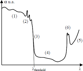
Physical absorption processes can be summarized as such:
– (1) interband transitions: high α and strong interactions with free carriers and photons in the crystal lattice, whose energy levels are situated outside the bandgap;
– (2) excitons absorption: high α, the exciton corresponds to an energy level Eexc (Coulomb energy) between electron and hole in the electron-hole pair created by photo excitation. This bond energy is lower than the bandgap energy, the electron and the hole can stay electrically interacting under certain conditions;
– (3) absorption of the bandgap: absorption of an optical signal to bring an electron from the valence band to the conduction band and thus free it in the lattice to participate in conduction. The created electron-hole pair is assumed to have no interactions;
– (4) absorption by the impurities present in the crystal;
– (5) intraband transitions: low α and optical absorption by free carriers in the lattice whose energy levels are situated inside the bandgap;
– (6) extrinsic excitation: low α and photo-ionization of impurities present in the crystal.
Figure 2.43. Direct transitions allowed (a), direct transition forbidden (b), indirect transition allowed (c), in a semiconductor as a function of the wave vector k
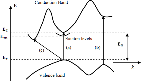
In this absorption process, transitions between valence and conduction bands are of the most interest. These occur in a direct gap semiconductor (if the peak of the valence band is in the same wave function plane as the conduction band minimum) or in an indirect gap semiconductor (the band extremes are not in the same plane). Thus four distinct transitions can exist and/or coexist (Figure 2.43) [KIR 75; SAP 90]:
– allowed direct or vertical transition: r = 1/2;
– forbidden direct or vertical transition: r = 3/2;
— allowed indirect transition: r = 2;
– forbidden indirect transition: r = 3.
Close to the threshold and depending upon its response, the absorption coefficient is written:
where α0 is a semiconductor and optical wave energy function constant, r is a transition dependent coefficient.
In the presence of excitons and phonons ((2) in Figure 2.42), the latter can participate in light absorption by interband transitions, corresponding to an absorption coefficient dictated by the Urbach equation:
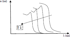
where σ is a coefficient between 1 and 3, dependent on temperature, Eexc is the exciton energy level. The Urbach equation accounts for the absorption coefficient above the threshold, when the absorption phenomena are no longer uniquely intrinsic between the valence and conduction bands but are caused by impurities whose energy levels are inside the forbidden band (Figure 2.44).
Figure 2.44. Near threshold absorption coefficient
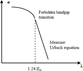
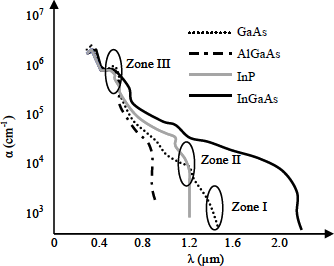
Figure 2.45 shows the absorption spectrum close to the threshold for different direct gap semiconductors. The three zones on the plot are easily distinguishable, zone I accounts for the Urbach equation, zone II close to the threshold accounts for intrinsic absorption of the semiconductor, and zone III accounts for absorption due to crystal impurities or by electrons found in localized states. This is characterized by more or less narrow absorption bands.
Figure 2.45. Near threshold absorption coefficients for different semiconductors
2.3.2. FKE
A compression or expansion of the crystal lattice produces a variation of the magnitude of the bandgap, causing threshold displacement, and hence, an intrinsic absorption band boundary shift.
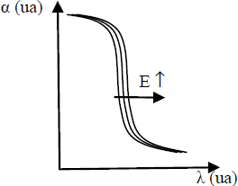
Also, the application of a strong electric field prompts a shift of this boundary towards large wavelengths, diminishing the magnitude of the bandgap energy: this is the FKE (Figure 2.46).
Figure 2.46. Threshold absorption shift due to an applied electric field: Franz-Keldysh effect
Thus by applying a high enough voltage on a semiconductor, the absorption coefficient can be increased for a given wavelength and thus increases the number of photo-generated electron-hole pairs. A typical Franz-Keldysh modulator can be composed of a Schottky diode or a PN junction reversely biased to create a strong electric field in the depletion region. The material used depends on the range of useful wavelengths.
2.3.3. Stark effect
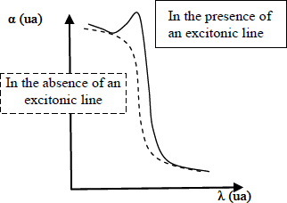
At low temperature and in a very pure semiconductor, or at ambient temperature in a quantum well-confined structure, the electron and hole can continue to interact electronically allowing a decrease of the photon energy required to create this linked electron-hole pair. In these conditions, there exists a fine absorption line with energies stronger than the semiconductor gap energy (zone (2) of Figure 2.42), corresponding to the generation of electron-hole pairs if the semiconductor is illuminated by photons with such an energy.
If an electric field is applied to the material, the pair level energy varies and a spectral shift of this absorption line is obtained, called the excitonic line. This is due to the Stark effect and is called the ”quantum confined Stark effect“ in the case of components using a quantum well structure. The magnitude of this absorption line depends on intrinsic parameters (exciton lifetime) and extrinsic parameters (crystal quality).
This shift causes a variation of the absorption coefficient as a function of the applied voltage at a given wavelength. Thus structures can be created, which by a more or less strong absorption phenomenon from a traveling light beam, will be able to transport an electric signal by modulating the light. An electro-absorption modulator is thus obtained.
Figure 2.47. Semiconductor absorption coefficient plot in the presence or absence excitonic lines
The biggest problem is that the strong absorption coefficient relies on temperature. As a result a negative temperature variation in a semiconductor, such as GaAs, causes a shift of its absorption coefficient towards blue, so towards smaller wavelengths due to the size increase of the bandgap. A steady temperature is constantly required around an electro-absorption modulator in order to function properly at the reference optical wavelength.
2.3.4. Quantum well structures
By creating a quantum well structure component (see section 2.1.9.4), excitons are confined to quantum wells and hence comparatively improve the Stark effects of a very pure intrinsic semiconductor. This results in an absorption coefficient that is a function of the optical wavelength and of the electric field applied for each quantum well.
Considering a quantum well in which there are no free carriers without excitation, the application of an electric field on the material will cause an absorption coefficient variation. Furthermore, after excitation, free carriers will be generated in quantum wells, contributing to an additional absorption coefficient variation. The well absorption coefficient variation can thus be divided into two parts: (1) due to the electric field and (2) due to free carrier filling of well energy bands. This variation as a function of the applied electric field is nonlinear.
These quantum well structures allow the creation of electro-absorption modulators named QCSE-EAMs (quantum confined Starck effect-electroabsorption modulators) [SCH 99; WEL 99] and MQW-EAM [CHI 92; HOJ 02].
2.3.5. MEA operation
The absorption spectrum in an EAM is very important and doubly dependant on the optical signal and electrical signal. The variation of its absorption coefficient, at a given length must be as large as possible on a biasing range.
It is equally important to minimize the modulator optical insertion losses by operating it at a biasing point corresponding to small losses. Thus the component will show a higher power reading than components showing strong losses linked to their biasing point.
This last point is less limiting if the EAM is uniquely used as an external modulator.
An EAM thus consists of multiple quantum well structures lit by an optical beam. These multiple quantum wells can themselves be inserted into an optical guide to increase the optical signal absorption length. Thus if the beam perpendicularly lights the layer comprising the quantum well, the absorption length is severely reduced. If there are multiple quantum wells, the absorption length is multiplied by the number of quantum wells, and to further increase it, multiple quantum wells are inserted into the optical carrier center (Figure 2.47). This structure is then inserted between 2 N and P-doped layers to constitute a PIN diode, which when reversely biased will create inside the layer i, composed of the multiple quantum wells, a strong electric field that will induce the absorption coefficient variation.
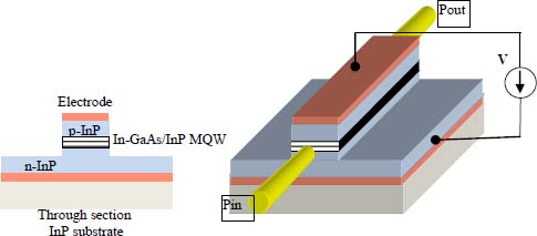
The optical power, Pin, injected at the EAM input is exponentially attenuated along the length of the optical guide made of multiple quantum wells according to the formula:
For a considered optical wavelength and assuming a constant temperature:
Thus at the exit of the modulator of total length Lm, the exit power is written:
It is relatively difficult to analytically determine the absorption coefficient as it is very nonlinear and dependant on the material, the temperature, and the optical signal wavelength. However, the optical response of the EAM as a function of the biasing voltage can be determined by measuring the output optical power, for a fixed input power (Figure 2.50).
Figure 2.50. Optical extinction ratio measured from an InP modulator operating at 1,550 nm [DES 07a]
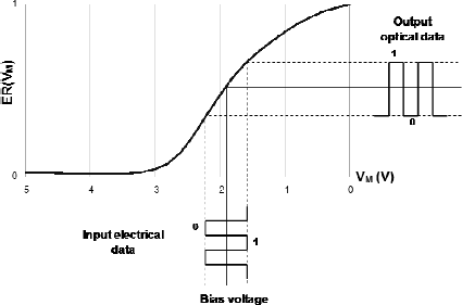
The optical extinction ratio is then deduced:
A response nearing an exponential and consisting of a linear zone is observed for a continuous biasing close to -2 V. If a sine or digital signal is superimposed on the modulator biasing, the optical power is then modulated and will convey the information to transmit. A very strong optical power attenuation at the EAM output can equally be observed if polarized below — 3 V, due to a very strong absorption in the optical guide. Thus the EAM can be used in this biasing zone at the cost of introducing very strong insertion optical losses. Similarly, if the biasing voltage is too close to 0, insertion losses are low but the amplitude of the modulated signal is limited.
The curve of the absorption coefficient as a function of the biasing voltage can be deduced from the measured curve of the optical extinction ratio (Figure 2.51).
Figure 2.51. Absorption coefficient of a modulator of 75 µm length on InP operating at 1,550 nm corresponding to the extinction ratio of Figure 2.50
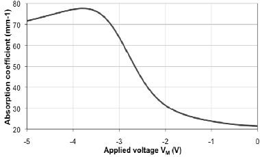
2.3.6. Characteristics of an EAM
The main characteristics determining the electro-absorption modulator performance are those of the electro-optic modulator:
– modulation efficiency: the modulation voltage value necessary to modulate the optical signal, measures the linear zone of the extinction ratio:
– optical extinction ratio: accounts for the modulator output power ratio at voltage V on maximum power, corresponding to a voltage of 0:
– optical insertion losses:
– chirp: corresponds to the frequency change of the carrier during the modulation of an optical wave, depending on the wavelength and the biasing voltage. The chirp in an EAM can be positive or negative by adjusting the biasing voltage.
2.3.7. EML: EAM integrated to a DFB laser
The main interest of an electro-absorption modulator is that it can be directly linked with a DFB laser to form an EML (electro absorption modulated laser) [GER 03; LIM 08; SRI 08]. The chip has two electric driving electrodes, the first brings the biasing from the laser diode and the second brings it from the EAM coupled to the modulated electrical signal. The output is purely optical: an optical beam modulated by a very high output signal. Figure 2.52 represents this type of structure.
Several physical phenomena are to be considered when evaluating such a circuit:
– the alignment at the output of the laser diode and input of the EAM, this optical coupling gives rise to optical losses increased by the propagation in the optical guide;
– the optimization of the EAM driving electrode shape, which must keep a large bandwidth in such a way as to increase the signal to very high speed [DES 07b; YAM 05];
– the dissipation of heat generated by the components while stabilizing the temperature in order to prevent thermal shifts to which the components are very sensitive. Thus a thick metallization for electrodes associated via holes connected to the ground plane must be used [BIA 03; YU 05].
Figure 2.52. EAM and laser diode integrated EML structure
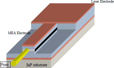
Integrated EAM have the potential for very high bit rates; in particular, they can modulate an optical signal at 43 Gb/s [CHO 03; CHO 07].
By introducing multiplexing techniques, bit rates in excess of 100 Gb/s can be achieved [CHO 07; LEE 04].
They operate at telecommunication wavelengths of 1,550 and 1,310 nm, mainly produced using InP technology.
2.3.8. EAM electrical modeling for ultra-fast signal simulation
High bit rate optical communications simulation software integrate EAM models. However, it is interesting to develop integrated nonlinear optomicrowave components in a microwave-integrated circuit simulator and a simulator system such as the ADS software commercialized by Agilent. Thus the dynamic electrical response and the electro-optic response of the component can be simulated.
A nonlinear electric model EAM has been developed [DES 07b, DES 09, ALG 10]. It accounts for:
– the EAM nonlinear electro-optic response characterized by its extinction ratio by considering that it can be expanded in the form of a rational fraction (Padé approximation);
– the dynamic response of the PIN junction constituting the EAM, equivalent to a RC circuit;
– the EAM electrode frequency response, very precisely simulated on Ansoft finite element method HFSS (high-frequency simulation system), a three-dimensional high-frequency simulation commercial software.
An equivalent electrical model integrating these three aspects allows the accurate simulation of an EAM electro-optic response, its frequency response in S parameters, and equally, the eye diagrams for different bit rates.
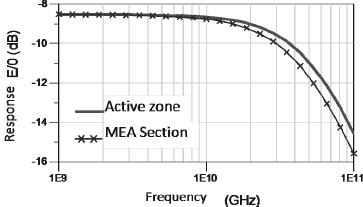
Figure 2.54. EAM output simulated eye diagram for bit rates of 10 Gb/s (unbroken line) and 40 Gb/s (dashed line) [DES 07a]
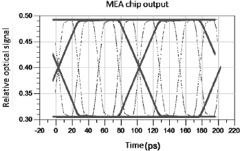
An EAM eye diagram can also be simulated for a bit rate of 43 Gb/s by using an ideal pseudo-random binary sequence from ”0“ to ”1“, generated by the simulation software (Figure 2.54). This simulation allows the demonstration of the EAM biasing point and the modulating electrical binary signal amplitude influences. Thus the appearance of asymmetry in the eye diagram, while straying from the biasing linear zone can be noted (Figure 2.56).
Figure 2.55. Transmission and reflection frequency responses, simulated on HFSS, from the EAM driving electrode [DES 07a]
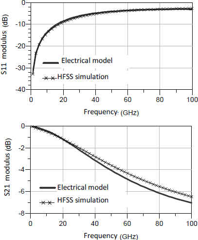
By introducing through simulation a real PRBS (pseudo random bit sequence) from a generator, an opening of the eye close to that measured is obtained.
This system can be integrated into a more complete high bit rate optical communications system, as shown in Chapter 7 of [ALG 10].
Figure 2.56. EAM eye diagram simulation at 43 Gb/s for an ideal PRBS and a biasing of -2.6 V, corresponding to operation in the linear zone