
25
Implementation
25.1 Introduction
This chapter will consider the various issues related to implementing the Bluetooth specification in real products. There are many conflicting design issues, tradeoffs, and the usual cost vs. performance vs. time to market problems which face any product development exercise. However, Bluetooth seems to face a larger and more bewildering array of such issues than most new technologies. This is due—in part—to the sudden explosion in interest from both suppliers and users of the technology and also to the technology itself and the overriding need for low cost and “out of the box experience,” which Bluetooth savvy people like to refer to. That is, Bluetooth-enabled products absolutely have to work reliably and seamlessly with no special configuration straight out of the box.
We start by considering the partitioning between hardware and software, and the types of engines which might be used to run software—i.e., microcontroller, DSP, RISC, or CISC. We then look at the various system design choices—i.e., one silicon device or two silicon devices and some key technical considerations—i.e., clock frequencies and silicon processes. We consider the radio design issues and finally the option of purchasing Bluetooth technology as an Intellectual Property (IP) core to add to an existing product development.
Although originally thought by many to be a relatively straightforward and simple system to implement, Bluetooth has proved to be more complex, especially if one wishes to realise a full implementation of the specification in an optimal way. Many developers have been working on Bluetooth solutions since 1998 with sizable teams of hardware and software engineers. The Bluetooth protocol stack is a complex multithreaded and multilayered piece of real time software, while the lower layer hardware component requires carefully designed autonomous state control and timebase management with a keen focus on power and cost optimisation.
Bluetooth is clearly not a simple system to implement. Though it is fair to say that if one only requires a point-to-point, low bandwidth link, perhaps suitable for a data synchronisation application, then a greatly reduced Bluetooth implementation can be much more straightforward. However, since the majority of applications end up requiring most Bluetooth features, the task soon scales upward.
The key tradeoffs to be addressed in successful Bluetooth system design are summarised below, and in common with most tradeoffs, there is neither a right nor a wrong answer. In this chapter, we aim to highlight these issues and illustrate the different tradeoffs one can make:
- Software vs. hardware partitioning.
- Single-chip vs. digital part + RF part.
- Software partitioning between embedded MCU and the host.
- Which profiles to support.
We also discuss how it is possible through the right design choices to meet the commonly highlighted target parameters for a Bluetooth-enabled product:
- $5 additional cost to the Bill Of Materials (BOM).
- Length of autonomy—many days on one charge: 10μs A Standby, 10s mA Active.
- Form factor—space for only one or two silicon packages.
- Seamless and easy Out Of Box Experience (OOBE).
25.2 System Partitioning
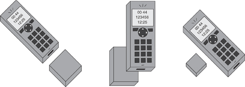
There are a great many ways of incorporating Bluetooth technology into a product. Early Bluetooth solutions adopted a simple add-on strategy using bought-in modules connecting to an existing product. The cellular handset market is an obvious example of this, and three common options are depicted in Figure 25–1. The first diagram shows the ubiquitous Bluetooth dongle, requiring no special support in the handset; the second shows a Bluetooth-enabled battery module requiring some handset support; and the third example depicts the most sustainable option for anything other than a quick market entry demonstrator, the snap-in or slide-in card.
This strategy is the lowest risk and shortest time to market, but of course, it has the highest cost, largest form factor and is the least integrated and seamless. An evolutionary path exists, where the module may be decomposed and absorbed into the product, and this is the likely scenario for handsets in particular. First, a complete module may be integrated onto the PCB. For major cost savings, the components themselves may be integrated onto the PCB using, for example, an RF module and separate baseband ASIC, followed by integration of the RF device and associated circuitry. At this point, there are several choices: absorb the Bluetooth digital part (baseband and MCU) into the system ASIC and add a simple RF device, or integrate the RF and digital parts together.
Figure 25–1 Handset add-on options.
It is interesting to note that as the Bluetooth market takes off at the time of this second edition, we are seeing a distinct move away from the dongle or plug-in module solutions in favour of PCB level integration. As the volumes rise, this is inevitable in order to reduce the cost to consumer levels.
25.2.1 Software vs. Hardware
The block diagram in Figure 25–2 shows once again the familiar protocol stack diagram. This time we are particularly interested in the interfaces between the various parts of the stack. To investigate the optimum partition between hardware and software, we must understand the requirements of each of the constituent parts.
The radio is, of course, unlikely to be implemented in anything other than hardware for some time yet. The baseband will need an element of hardware to at least control the basic on-air symbol timing and radio-enable strobes (RxOn, TxOn, SynthOn, etc.). However, many of the baseband operations such as bit stream processing, encryption, and frequency hop calculation are quite suitable for implementation on a Digital Signal Processor (DSP), if not on a MicroController Unit (MCU). Although modern MCUs such as the ARM7 are reasonably well-equipped in this area, taken as a whole, the Baseband Layer represents a sizable task if implemented on a processor, requiring a large number of “processor MIPS”.
The most interesting area for partitioning is between the Baseband Layer and link control level. This requires a lot of decision making and context switching between links, but it is extremely time critical to get the right information programmed into the radio in time to be active on the next slot. We saw in the earlier link control chapter how the LC state machine had to switch context many times and often in a very short space of time.
Figure 25–2 Bluetooth protocol stack.
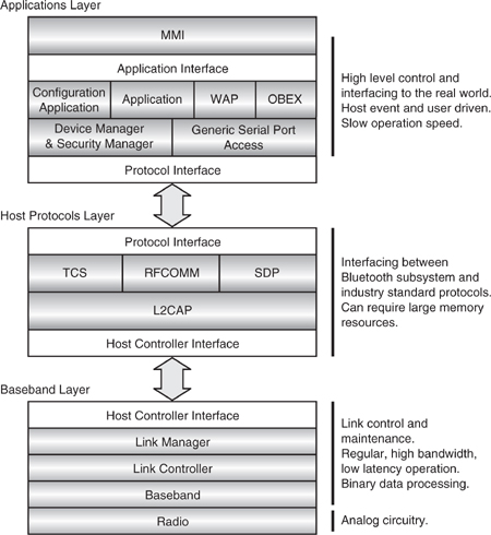
The next layer up the stack, the LM, is relatively time independent, with most LMP operations being self-timed and carried out across several time slots. The HCI is a well-defined part of the specification and therefore a sensible place to make a natural break in the stack. HCI commands are available for link establishment and clearing down and controlling the various aspects of Bluetooth, such as audio and encryption. The defined HCI transports provide a standard way of physically interconnecting two devices with an HCI interface, and indeed, the specification has been written with this split between the Blue-tooth module and the host device in mind.
The diagram attaches some arbitrary but useful names to the separate parts of the stack. The Baseband Layer is the part which exhibits time criticality, requiring knowledge of Bluetooth slot timing and is very bit-operation intensive. As such, it is typically part of the embedded Bluetooth entity which would reside in a Bluetooth module. The Host Protocols Layer is so called as it would most commonly reside on a host, such as a PC or handset. This provides an interface between Bluetooth HCI to a higher layer standard, together with data segmentation and re-assembly. This layer is not time critical, but can have large buffering requirements and be very memory intensive if dealing with large host data packets. As such, it may not really sit well alongside the lower layers in a single, embedded CPU. The Applications Layer consists of the high-level management entities and user interface, which interface closely with the Host Protocols Layer.
25.2.1.1 Software Considerations. It is useful to provide an indication of the magnitude of the baseband layer task. Assuming a full software implementation of LC, LM and HCI running on a RISC MCU, then a fully occupied system (multiple slaves, SCO links, Scan and scatternet operation) would require around 10 to 15 RISC MIPS.1 This means that at worst case system loading, an embedded RISC MCU such as the ARM7 running at 20 MHz will be fully occupied running the baseband layer protocols. Placing some or all of the LC state control in hardware will greatly ease the burden on the processor, but at the expense of increased risk and decreased flexibility.
1Millions of Instructions Per Second, where each instruction is a simple operation such as is typical in a Reduced Instruction Set Computer-type MCU.
The complexity of the stack makes use of a high-level language such as C and some kind of Real-Time Operating System (RTOS) essential to provide the necessary interprocess communication, resource scheduling, and debug facilities. As explained below, latency is so critical for Bluetooth, as is footprint (i.e., memory usage, etc.), that the choice of RTOS is another critical factor. Increasing processor speed and performance cannot unfortunately be relied upon to ease the situation. As for most Bluetooth applications, ultra-low power operation and low cost are paramount. These are also strong reasons why a DSP implementation is not generally attractive, others being that most of the stack requires operating system support, context switching, and large address range operation, all of which are not generally available from a DSP.
The timing diagram in Figure 25–3 shows how critical a task the link controller is. The diagram shows the end of a receive packet protruding into the current slot. The worst case figure given is that for an ID packet received in the second half of the slot (312 + 72 μs). This is, of course, a specific case during page, inquiry, or unparking. However, in an ordinary connection, the worst case packet end is only slightly better at 376 μs for a DM3. The transmission itself could be offset by up to 10 μs and still be successful due to the uncertainty window. Following reception, the baseband must notify the LC (typically via an interrupt), which must then examine the relevant status information to ascertain what to do in the next slot. Among the various decisions to be taken are:
Figure 25–3 Link controller time criticality.

- Was the previous Tx successful and can new data be transferred to the Tx buffer?
- More importantly, was the packet just received something unexpected—an LMP control message overriding what should perhaps have been an SCO slot?
This latter example will most definitely alter what the device now does in the very next slot. The LC processing must complete and program the baseband and radio in enough time to allow the radio to be ready for the next slot. Since the frequency hop will depend directly on the baseband state, and this will depend on the previous packet received, the LC has only 625 – 180 – 384 – 10 = 51 μs to do this—a very short space of time, especially if it is operating as an Interrupt Service Routine (ISR) on an MCU also running a RTOS.
The diagram allocates a further 3 μs to the baseband to allow for any setup or pre-clocking required, such as buffer switching or synthesizer data serialization and 180 μs to the channel synthesizer for frequency settling. Clearly, reducing the synthesizer's settling time can increase the LC time. However, commercial solutions are in the range 150 to 200 μs, and 180 μs is fairly typical, so there is a limited degree of flexibility here. A faster processor will “cram in” more processing within this critical window, although another constraint exists: the lower priority background task of scheduling the other links, other LC tasks, and transferring data into and out of the baseband. This task is difficult to speed up as it is only driven by the end of the Rx or Tx burst and will probably be active for most of the slot. Again, it must complete before the next Tx or Rx begins.
25.2.1.2 Hardware Considerations. Figure 25–4 shows an example baseband system block diagram. Although similar to the diagram in the baseband chapter, it includes an interface to the MCU, which executes the protocol stack software. This would typically comprise a register set, interrupt control logic, and probably a Direct Memory Access (DMA) engine to provide faster2 memory transfers to and from the buffer memory. The buffer memory itself is shown as one block since this is more area efficient and thus cost efficient in silicon terms.
2Most processors will take more than several cycles to first read a memory location, then write to another, increment a counter and loop. This all makes the time criticality worse, whereas a DMA engine will typically transfer a complete word in one or maybe two cycles.
Figure 25–4 Typical baseband block diagram.
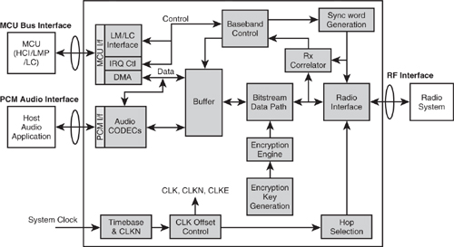
The “Baseband Control” block is so named because this may contain some or all of the link control protocol and state machine. In some implementations, this consists of a basic state machine driven by a software link control task. The advantage of this is lower risk, less complex hardware, and more flexibility, at the expense of a heavily occupied MCU. At the other extreme, some implementations place most or all of the link control task in this control block. This has the advantage of using much less of the MCU, which is running the remainder of the stack; however, at the expense of a very large silicon area and with much greater risk and less flexibility.
Several of the blocks shown may be implemented in software, particularly if the MCU is actually a DSP device. The prime candidates would be the audio CODECs, bit-stream processing, and hop selection, although the on-air data rate would need to be maintained and/or additional FIFO buffering might be required.
Some of the questions to address in getting the software/hardware partition right are listed below:
- Is the task too fast to be carried out by software?
- Is the task very bit-intensive and not byte/word-oriented?
- Is the task too complex to make a hardware implementation efficient?
—In silicon area or in power consumption? - Is the task too ill-defined or complex such that the risk of “hard-wiring” it into silicon is excessively high?
—Due to the risk of mistakes or of the specification itself changing?
25.2.2 Where to Run the Host Protocols
As discussed already, if we implement the LC protocol in software and require a full Bluetooth system, we may not have much processing bandwidth left for the higher layers if we are using a small, low-power, embedded processor, such as the ARM7, Hitachi H8, embedded Power PC, or Motorola Dragonball, to name but a few. We could adopt a much higher performance MCU such as the ARM9, Hitachi SH, or similar, but these do not currently3 fit the target low-power or cost parameters we listed above.
3But naturally, this will change. Over the next few years, CPU performance and power efficiency will increase dramatically, facilitating a complete solution in one processor, though there are other reasons for optimising the partitioning as described here.
The following numbers are just lower and upper bounds gleaned from an overview of the various solutions and partitions currently on the market and serve to illustrate the issues driving the question of partitioning. The actual point in the range, especially the baseband end, depends on the exact partitioning used. For example, the Baseband CPU can also be handling some of the low level Baseband control and Bitstream data processing in order to reduce associated hardware gate count. It is also important to note that although easy to grasp, such MIPS estimates can be dangerous, as they give no indication of latency or instantaneous peak load requirements.
Baseband Layer (Some Baseband functions, LC, LM and HCI): 8 - 12 MIPS
Host Protocols Layer (HCI, L2CAP, RFCOMM, SDP): 1 - 2 MIPS
The Applications Layer requirements are very difficult to quantify, as they depend largely on the other protocols and/or services defined by the relevant profile. A headset, for example, will impose a minor additional processor load, while a LAN access point with IP routing and large Segmentation and Reassembly (SAR) requirements will exhibit significant additional processor loading.
As each of the embedded low-power processors listed above provides around 10 to 30 MIPS with acceptable power consumption, the stack may just be squeezed into one such CPU running at its maximum performance level. However, it is unlikely that any resource will be left to run any interesting applications in. The latency issues alone make integration of any other real-time system (especially a cellular telephony standard like GSM) a very difficult exercise requiring much more than just the sum of the respective MIPS!
One solution to this is to run different parts of the stack on different processors. Figure 25–5 shows three different ways of splitting the stack for different applications with different requirements.
Figure 25–5 Different stack splits.
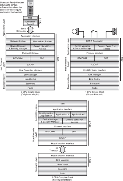
The first is the classic handset add-on solution. A complete Bluetooth subsystem is implemented in the add-on; however, since only the headset and dialup profiles with point to point connectivity are required, the entire stack up to the application level can be run on one CPU. The L2CAP task, which requires much buffering for Segmentation And Reassembly (SAR), is greatly simplified in this case, and the data bandwidth required is quite low (14.4 kb/s for GSM). The host processor in the phone, however, will require some MMI and control application to interface with the Bluetooth stack. This is relatively straightforward and easily implemented alongside the GSM stack since it has no real-time components.
The second example is a typical headset with only a microphone and switch as inputs and a speaker as output. Since the L2CAP, SDP, and RFCOMM components are minimal for such a simple profile, they are easily implemented all together in one CPU. Only one link is likely and, quite probably, multislot packets will not be required. In fact, for an optimal solution, the entire Host Protocols and Applications Layers may be integrated into one “headset” application program.
Finally, the third example is of a complete, fully featured stack where the Baseband Layer resides in one embedded CPU, but since this does not have sufficient spare resource, the Host and Application Layers are run on the host CPU. This represents the case in a PC where the HCI USB transport might be used to provide a clean industry-standard interface to many other devices and systems and is the reason for the natural break in the stack at the HCI. The upper layers are then run on the PC, PDA, or Smartphone, where they happily reside alongside the myriad of other software tasks running on a relatively high-performance CPU.
25.3 Hardware Integration Options
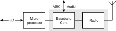
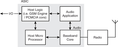
Having decided on where to split the software tasks, we must still decide on the physical partitioning of the system. We need an MCU and associated memory to run the higher layers, a baseband logic core, and a radio system. Typically, we will embed the MCU and memory within the same silicon Application-Specific Integrated Circuit (ASIC), Figure 25–6, to create a baseband to the HCI core with an embedded CPU running the stack up to the HCI and add a separate RF transceiver device. However, we may instead wish to use an existing host MCU.4 Figure 25–7 shows such a partition where the baseband core sits alongside the radio system as a Bluetooth transceiver device with a standard processor bus interface. However, this latter example is difficult to realise due to RF/digital integration issues, which we will look at in the section on the single-chip solution.
4Providing one is available with enough residual resource and performance, or perhaps we have implemented much of the critical LC protocol in the baseband logic core.
Figure 25–6 Two-chip solution: baseband to HCI + radio transceiver.

Figure 25–7 Two-chip solution: micro + baseband and radio transceiver.
25.3.1 Two-Chip Solution
At present, commercially available two-chip solutions revolve around separation of the RF from the baseband, since the RF function is typically implemented in BiCMOS (slightly larger area and more expensive, but easily realises the required RF performance) and the digital part in CMOS (smaller, cheaper, lower power, but without the performance necessary for RF). The interface to the digital part is then direct PCM and HCI via a high speed UART and / or USB transport.
The BlueRF initiative is of major importance here since a standardised interface between the baseband / LC device and RF device will drive the market for such parts immensely due to the multiple sourcing flexibility it provides. Many RF device manufacturers are claiming BlueRF support, and the SIG looks set to adopt this as the industry standard Bluetooth RF interface. This allows different solutions to be easily used from various suppliers featuring different performance/cost tradeoffs and features with a standard interface. Furthermore, one product can be specified with several different radio options, as required.
25.3.2 Single-Chip Solution
The holy grail of Bluetooth implementations is the so-called single-chip solution, which is illustrated in Figure 25–8. Here the digital baseband to HCI part and radio are all integrated into one device. This device may also feature support for applications, such as headset circuitry and the entire stack required for that profile as depicted in Figure 25–5.
Figure 25–8 Single-chip solution.
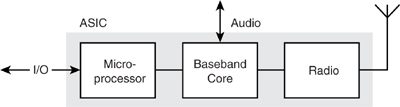
Figure 25–9 shows an example of how a single-chip device could be laid out. The key issue is the integration of RF onto the same die as the digital circuitry. Two problems must be overcome:
Figure 25–9 Single-chip layout.
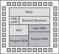
- CMOS is the only cost effective option for the baseband (a large digital system). The standard CMOS process must be improved to provide the necessary low noise and high Ft5 (Transition Frequency) required for RF circuitry. Also, additional silicon processing (typically only one further polysilicon layer) must be added to facilitate the construction of passive components such as capacitors.
- Interference and noise injection from the digital circuitry into the RF via the silicon substrate must be prevented.
5Transition Frequency (Ft) is the linear bandwidth of operation provided by the transistors. It defines the frequency performance of a process. For a 2.5GHz RF transceiver, a minimum Ft of 25GHz is necessary.
The advantages of a single-chip solution are reduced cost, smallest footprint, and an “off the shelf” solution with less knowledge or design-in of RF circuitry required. Manufacturers provide reference designs, following these gives the simplest route to a qualified product. (Implementers who lack in depth radio experience should take great care when using reference designs, as even changing the source of a component to substitute one which is apparently equivalent can subtly alter characteristics so that system behaviour changes.)
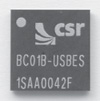
There are some disadvantages of single chip solutions. Less RF flexibility is possible, although it is possible to add an external PA for +20 dBm operation. There are limited possibilities to gain access to the processor, although chips such as the one illustrated in Figure 25–10 can have user applications added, the memory and interfaces available are limited. Finally, no further integration into a system ASIC is possible.
Figure 25–10 Single-chip device (Courtesy of CSR).
Optimised RF processes, such as BiCMOS, are not far behind digital CMOS processes in size and cost; especially RF capable CMOS. So, assuming similar volumes for RF only devices and integrated single-chip devices, an RF only device may allow a lower footprint and cost implementation where integration of the digital baseband circuitry into a larger scale System On Chip (SOC) ASIC is possible, along with other system blocks, as shown in Figure 25–11.
Figure 25–11 Fully embedded solution: SOC ASIC + radio transceiver.
25.3.3 Fully Embedded Solution
This approach is ideal for complex products such as digital cameras, cellular hand-sets, PDAs, game pads, etc. where a large-scale ASIC is used to integrate the system-level block functions together. The addition of a small RF transceiver is all that is required on the PCB, together with a handful of passive devices. This of course also provides us with the same RF advantages of the two-chip solution and allows Bluetooth to be added as a PCB option in manufacture (albeit with some overhead in the SOC ASIC).
With time, the risks and additional cost associated with integrating the RF part will be reduced. However, there will always be advantages attached to the separate radio transceiver solution for certain applications such as the opportunity to integrate digital circuitry into an SOC ASIC, the flexibility of RF supply, and the possibility of higher performance RF on better silicon processes than is possible with the single-chip solution. As is usually the case, there is no one right answer!
25.4 Bluetooth as an IP Core
We now consider an extension to the SOC solution presented above, that is, inclusion of a third-party-supplied Bluetooth core. The opportunity to be in at the beginning and the sheer size of market predictions for Bluetooth have attracted a number of companies into the field of Intellectual Property (IP) design and licensing. As described at the beginning of this chapter, the development effort, and in particular, the elapsed time demanded to produce a Bluetooth solution are sufficient to make the cost and time to market issues related to licensing a Bluetooth IP solution a very attractive proposition indeed.
There are several suppliers of such products, each with a different background, product partitioning, feature set, and business model. Indeed, the size of the potential market seems to encourage discussion and to some extent cooperation among what is likely to become a very competitive sector of the marketplace.
25.4.1 Why IP?
The advantages of adopting an IP solution for any new technology development are reduced time to market, higher levels of integration through SOC design, and a very low Bill Of Materials (BOM) as the cost is reduced to the additional silicon area only. It is important, however, to recognize that some form of license fee will be payable.
The IP supplier should warrant the core to the Bluetooth specification, and through some form of maintenance agreement, maintain the design and supply updates and improvements both as the specification evolves and as the supplier improves its product. In addition, the licensee will benefit from the detection of any bugs and inconsistencies in the core by all other licensees, so they should realise a better quality product over time.
Bluetooth is an enabling technology with applications across a whole variety of products. A great advantage of an IP solution is the possibility to reuse the one core many times, realising new product solutions quickly and easily. Maintenance of the core technology is centralised, with minor variants to the central design easily made and then usually only involving the external interfaces. The increased volume of several product lines combined also facilitates amortisation of the license fees across what is now a very large volume of units.
25.4.2 What Are the Issues?
There are some risks attached to such a solution. Any “bought in” design must be integrated within the design team, the tool environment, and the company methodologies. Dealing with another organisation as an IP supplier adds management and logistical issues. The question of quality and functionality of the supplied core is also important, as is how problems or bugs get dealt with and fixed.
Any IP core must—just like Bluetooth itself—be “Plug & Play”. The supplied core must be complete and ready to use. Design transfer, support and training, and documentation are important. The use of generic or easily redesignable interfaces is also important, as each system’s requirements are different. The core must be capable of integrating into the SOC with a minimum of effort to deliver the promised fast time to market and low risk.
Confidence factor is another key issue, as licensees need to be convinced of success. This will probably be provided by demonstrator kits, reference designs, and ultimately, design-win examples.
If an organisation is going to buy source code, they have the right to expect a quality product in both form and function, so the quality of coding style and documentation is arguably even more important than for an internal development. After all, someone else is going to have to pick up the code and work with it. Some kind of warranty will be expected, and in most cases, suppliers guarantee conformance to the latest version of the Bluetooth specification.
The design itself must be able to cater to all possible requirements of the various customers who will use it while meeting the cost needs of the lower specified products, so a full implementation is probably important. This is a major area where suppliers must work hard to differentiate themselves—providing services and/or solutions to meet the exact needs of each customer.
25.4.3 Source Code Supply
A complete solution is essential. This should comprise a full design hierarchy of well-documented code following a consistent style guide, a full documentation suite at both the module and system level, and a full set of compile and (for hardware) synthesis scripts, including reference constraints for specific processes. The design should also be supplied with a set of module-level test benches where appropriate and a suite of system verification test benches with accompanying reference data to validate the major areas of functionality, such as inquiry, paging, and all packet types used in connection, etc.
The baseband is most likely to be supplied as Register Transfer Level (RTL) VHDL, or Verilog code, and the protocol stack software as portable ANSI C code. Both of these are industry-standard, portable design formats.
25.4.3.1 Baseband Core. The design must be “tool-friendly” and well structured. Automatic Test Pattern Generation (ATPG) tools and synthesis tools require that certain design rules have been followed to deliver good results. A modular design approach provides easy redesign for specific interface requirements and resizing of the memory requirements and silicon area if certain features are not required, such as encryption, for example. This might include porting of the design to support a different MCU, radio, or audio subsystem.
Subsidiary functions may be useful if included, such as MCU peripherals, audio circuitry, and LPO control circuitry to remove the need for additional components, i.e., “just add MCU and memory!” If the supplier is a “one-stop shop”, also supplying the complete software stack, then different protocol software/baseband partitioning may be possible, allowing MCU resource vs. performance to be traded for specific implementations.
25.4.3.2 Protocol Stack Software. Again, modular and well-structured code is important. The choice of RTOS is also very important, particularly as in most cases, the licensee will be looking to add their own code and so they will either wish to reuse their existing choice of RTOS or will be adopting the IP vendor's choice. For these reasons, it is advantageous if the software IP is written to use a Generic Kernel Interface (GKI), as shown in Figure 25–12. This itself is a difficult exercise to get right as we now have an RTOS and a thin API layer above it, which risks increasing the software load and latency issues. However, if implemented well, there are many benefits, such as:
Figure 25–12 Generic kernel interface (Courtesy of TTP Communications).
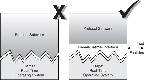
- Portability to different RTOSs by porting only the GKI and simply recompiling the stack.
- A common and reusable API presented to the stack (and any application) software.
- Integrated test features built into the GKI, which aid third-party integration and testing.
25.4.4 The Radio
A generic solution must support or be easily configurable to support all interfaces required by the various licensees. The radio is where this is most manifest as there are a number of different ways of interfacing to the radio and a number of different radio solutions available. Everyone has their own preferred radio solution based on different requirements and commercial pressures. Given the plethora of choices and interface options, a clean generic interface that easily facilitates redesign is the most flexible solution. A “soft” or reprogrammable interface will support some options, but there really are too many emerging to make this generally viable. Since Bluetooth RF requirements are not onerous with a binary digital interface and simple channel synthesiser programming, a simple interface can be easily retargeted with an optimal implementation each time.
The BlueRF initiative will have a strong positive influence on the use of IP solutions in the same way as described in section 25.3.1. Having procured an IP baseband and protocol stack solution, the remaining part of the puzzle—the RF—which is not easily integrated onto the same silicon anyway, will be available from many different suppliers with a standard interface to the supplied IP core.
25.4.5 Reference Designs
Turning the supplied IP into a real product is where the challenge lies. If the IP option is to prove advantageous in the long run, then the route to a product has to be rapid, easy, and low in risk. A key way for an IP vendor to enable this is to provide a “worked example” of the IP in the form of a reference design. Of course, a specific implementation will not be appropriate for all system solutions, but a good, well-thought out reference design or family of reference designs should be useful as a basis for the licensee's system design, and should greatly speed the product development cycle.
The reference design should be well proven, and indeed, will probably double as a technology proving platform and a sales and demonstrator tool. A well-designed and fully functional demonstrator will build immense confidence and will allow preconformance testing on the IP core itself, leading to possible precertification.
However, to be useful, it must not impose artificial constraints on a customer’s product design, such as locking a designer into using a specific interface device or MCU simply because that’s what the reference design uses and the IP solution has been designed to work with. A further risk is that adopting the reference design limits the possibility of product differentiation, although this may be provided by the MMI or application software design. In any case, a tradeoff may usefully be made here between product differentiation and time to market.
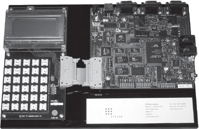
Figure 25–13 shows a typical Bluetooth reference platform. This uses a standalone ARM7-based MCU, a Xilinx Virtex high-performance FPGA containing the baseband IP core, and FLASH ROM containing the protocol stack software IP. This particular board also incorporates an MMI control board for standalone use.
Figure 25–13 Bluetooth evaluation board (Courtesy of TTP Communications).
25.4.6 Design Services
Major reasons for adopting an IP solution are time to market, resource shortages, and risk reduction. It is therefore valid to ask, “Why not outsource the whole Bluetooth subsystem, including modifications to the IP?” Indeed, the best people to modify the code and work with it are those that designed it in the first place. A common scenario is that a company wishes to absorb the technology themselves over time, but at least the first generation products need to be brought to market quickly and risk free, even if they are less differentiated and more costly. It is, therefore, quite common that an IP vendor will be asked to supply services to go with the IP. In fact, some suppliers only supply the IP as part of an overall design services package.
These services are likely to include modifications to the core (especially to the system interfaces), porting of the software to a different MCU, baseband synthesis to the customer’s chosen ASIC library including production test and ATPG generation, and assistance with production test and verification, or working sample approval. Finally, when ready, the vendor must supply sufficient training and design transfer support to ensure that customers are able to modify and maintain the code themselves when or if they wish to.
It is an interesting paradox that often the licensee wants to own the solution but does not want to modify and maintain it. The reassurance of knowing that the designer is on hand as required is very valuable indeed!
25.5 ASIC Prototyping and FPGAs
It is most likely that the final implementation of the baseband core is likely to be in silicon as a custom or semi-custom ASIC. However, it is highly desirable to validate the hardware and software together as a system before “tape out” of the costly silicon design, and as with most real time systems, this is very difficult to do in any meaningful way without some kind of hardware prototype being built.
Field Programmable Gate Arrays (FPGAs) have been around for some time, but they have tended to be very slow in performance terms and difficult to fit any complex design into due to their lack of internal resource. Furthermore, they have always required the adoption of specific design rules, which really do not follow good ASIC design practice. However, this has changed dramatically in recent years. Due to orders of magnitude, increases in performance, and greatly improved architectural design, the latest state of the art devices such as the Virtex series from Xilinx or the Apex series from Altera offer true SOC capabilities. Performance is on a par with ASIC processes of only a couple of generations ago and no specific design rules have to be adopted other than just good ASIC design practice. For a technology such as Bluetooth, which is not terribly demanding of current ASIC technology, a good FPGA implementation is very feasible.
Most Bluetooth IP suppliers at present have demonstration systems that utilise high performance FPGAs, and these are able to promote confidence in the IP, prove the technology, and provide better coverage of bugs and system testing. Of course, there are some “porting” issues to be addressed when moving to an ASIC implementation such as embedding what was an external MCU and moving from the internal FPGA RAM to an embedded ASIC RAM block. It is particularly important to ensure that enough validation is carried out on the ASIC design itself and not just to rely on the lab bench verification of the FPGA-based system.
Although FPGAs are expensive, due to their low risk, fast turnaround time, and flexible nature, they can provide a viable product route in themselves and make a pragmatic solution for low-volume, high-value products.
25.6 Making the Right Design Choices
25.6.1 Profiles Support
Specific applications require support of a particular Bluetooth profile or set of profiles, and each profile in turn will demand a certain set of protocols and features. For example, OBEX is not required for the headset profile, whereas the telephony profile requires the addition of the whole TCS stack.
All profiles are layered on the Generic Access Profile, shown in Figure 25–14, which includes requirements for certain parts of the specification such as Master and Slave operation, ACL and SCO link support, and encryption support. Other profiles add their own requirements on top of the Generic Access Profile.
Figure 25–14 Layering of profiles.

This makes it very important to be precise about what functionality is required in any implementation; adding support for another profile could suddenly bring a whole lot of baggage with it. The whole topic of profiles is a complex one. However, the SIG is planning to enable Bluetooth developers to create their own tailored profiles, which will enable specific optimal designs to include only the parts of the specification required for that specific application.
25.6.2 Memory Requirements
For any optimal solution in cost, size, and power consumption terms, memory usage must be reduced to the absolute minimum. RAM is more expensive in all these respects than ROM, and the data buffering requirements of Bluetooth can be quite large. We have already seen that L2CAP can become very memory-intense when supporting multiple high-bandwidth links driven by a networking application with a large packet size.
Currently, manufacturers are nervous about committing to a specific software code set in a masked ROM, and so most implementations—even current single-chip solutions—use FLASH. Since ASIC processes on 0.25 m and better have recently added FLASH cores as a standard library component, this is not such an issue. But, of course, it isn’t free.
The range of memory requirements exhibited by different implementations is quite diverse and driven mostly by the hardware / software tradeoff. However, other factors are also important, such as coding method and specific processor architecture. As an example, a design based on a large operating system might require 256 kB of ROM and 128 kB RAM, whereas a carefully hand-coded system using a small RTOS may use 128 kB ROM and 32 kB RAM. By reducing the segmentation and reassembly load on L2CAP, the RAM figure will drop noticeably further.
Although the LMP specification makes reference to the use of Nonvolatile RAM (NVRAM), it is desirable (and indeed the SIG has worked to avoid the need for it) to not require nonvolatile data storage. Real-time FLASH reprogramming is not straightforward and the presence of FLASH cannot be relied upon anyway. Other NVRAM technologies are not readily integrated on silicon and will add cost if implemented on the PCB. Therefore, it is highly preferable to avoid the requirement for NVRAM at all. This imposes restrictions on the high-level functionality of a device, as it may need to pass important information to the host for storage, or always require reconfiguration after a power down, for example.
25.6.3 Clock Requirements and Low Power Considerations
The choice of system clock has important ramifications. In cellular applications, 13 MHz is a common frequency; in office equipment, 10 MHz is common. Computing equipment such as PDAs, laptops, etc. use clock frequencies such as 33 MHz, 50 MHz, 66 MHz, or more. Since extra crystal oscillators add PCB area and cost, it is desirable to use the same system clock reference for the MCU, baseband processing, and the 1 MHz symbol timing; however, this requires that it must be accurate to ±20 ppm as defined in the specification. Running a system at a high clock rate increases power consumption, and so unless the clock to parts of the system can be turned off when they are inactive, multiple divided down clock domains may be required. This complicates the design and so has to be balanced against the power savings if the reference clock is large, say above 50 MHz.
The low-power modes defined in the link control protocol allow the system to lie dormant for a period of time, but still require the Bluetooth clock counter, CLKN, to be maintained with a 32 kHz reference, which is specified to be tolerant to ± 250 ppm. It is crucial that this crystal stays within this accuracy during its life or is calibrated in some way to maintain robust operation. It is also important when in low-power mode that everything on the PCB that can be turned off is turned off so as to maximise power conservation.
As process voltages drop and battery technology improves, design techniques have to be more rigorous to deal with the lower operating voltages which result. In addition, below 2.7 v, the range of different operating voltages becomes larger and different devices require level shifting and DC-DC conversion to work together, both of which add cost and power consumption. Battery technology has always evolved slowly, but in the next few years, lithium ion will become commonplace, even for cheap consumer products, while new technologies like lithium poly will become available for longer autonomy in higher end products.
25.7 Radio Implementation
Existing RF architectures for general purpose ISM or DECT applications are relatively easy to bring to market quickly in support of Bluetooth. However, due to various factors, Bluetooth specific RF designs can be made smaller, cheaper, and lower in power. In some ways, they need to be more complex to deal with certain Bluetooth specific issues such as the very short DC-free preamble. DC thresholding is much easier in DECT, as this uses 16 bits with an uncertainty window of ± 10 bits. Bluetooth’s 4 bit preamble, however, demands a new mechanism for both DC thresholding and receive clock recovery. The Philips UAA3558 part is an example of a DECT-based RF device which has been optimised to create a Bluetooth transceiver. By contrast, the Philsar 2401 is a clean sheet design that was targeted at Bluetooth from the start and has been designed on SiGe to offer robust operation in a fairly hostile environment.
Suppliers of radio devices are optimising their products to meet the cost and performance needs of Bluetooth with new architectures and techniques being developed to create optimal solutions in the following areas:
- Robustness—Advanced dynamic gain control, distributed gain stages, and fast DC thresholding
- System performance—Fractional N synthesiser design
- Lower power—Removing the need for mixer stages, increasing sensitivity, and lowering noise.
BiCMOS is the most popular choice for radio devices due to its low cost, which is almost as low as a digital CMOS process. However, some implementations use other processes; the Philsar device is based on SiGe, which gives lower power operation with lower noise and better sensitivity. CMOS has already been mentioned as an RF process in the section on single-chip solutions, where the issues of RF signal performance were discussed. However, as CMOS process voltages drop to conserve power, it becomes harder to maintain the low noise and high enough Ft for RF operation on the same silicon.
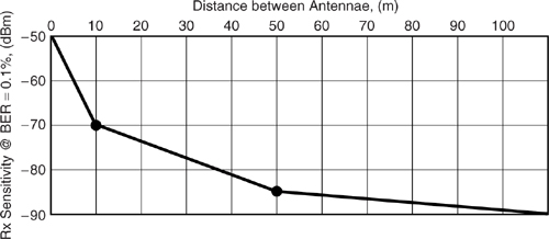
Figure 25–15 shows how increasing receiver sensitivity gives longer range operation. Two points are plotted: the Bluetooth-specific -70 dBm figure, which gives 10 m operation, and the higher value of -85 dBm, which some suppliers are specifying and which leads to claims of a huge increase in ranges up to 50 m. Moving to a more power hungry +20 dBm transmitter is not the only way to increase range. Clearly, in either case, both devices must share higher sensitivity or Tx power if a long range link is to be realised.
Figure 25–15 Receiver sensitivity vs. operation range.
Bluetooth’s RF requirements are not overdemanding of modern radio design and process technology with their simple binary digital interface and channel synthesiser programming; however, there are some issues to be kept in mind, such as the DC thresholding, receive clock, and data recovery and fast synthesiser settling requirements. Furthermore, more than other communication systems, the radio link must be as robust as possible to cope with the many interference sources present, the low link budget, and the low modulation index. In addition to all these factors, it must still maintain the user's “quality experience”.
25.8 Summary
We have looked at a range of issues concerning the realisation of a functional and optimal Bluetooth-enabled solution for a variety of applications. The choices and tradeoffs are myriad, and competing solutions aimed at addressing them are numerous. However, there are some definite conclusions one can make:
- The quality of “user experience” is very important and must be designed in.
- The target application must be well understood and specified.
- Any commercially successful implementation must be tightly optimised for cost and performance.
- SOC ASIC design should not be shied away from. There are very good sources of IP for Bluetooth, but they are not free and must come with a complete package of services and support.
- Standardisation of interfaces will make Bluetooth system design and implementation easier and the market larger.
- Bluetooth needs to be very high volume and thus has to be very low cost.