Chapter 11: The NXP LPC55S69 a reference IoT microcontroller
Abstract
In this chapter, we will look at a real-world microcontroller and the ideal hardware feature set required to support the PSA security model. For the purposes of this chapter, we will use the NXP LPC55S69 as a reference Cortex-M33 microcontroller. The LPC55S69 has a security structure on three levels, compute environment, device security, and assistive security peripherals.
Keywords
IoT microcontroller; Secure bus matrix; Security sideband signal; Master security wrapper; Peripheral protection checker; Security architecture; Trusted; Execution; Environment
Introduction
In this chapter, we will look at a real-world microcontroller and the ideal hardware feature set required to support the PSA security model. For the purposes of this chapter, we will use the NXP LPC55S69 as a reference Cortex-M33 microcontroller. The LPC55S69 has a security structure on three levels, compute environment, device security, and assistive security peripherals (Fig. 11.1).
The first requirement for our microcontroller is the ability to create a secure compute environment. This means that we need to extend the TrustZone partitioning to all the other bus masters within the system. Here, bus master means any unit within the microcontroller that can initiate a memory transfer. This will typically be DMA units and additional secondary processors. In order to achieve this, the microcontroller must provide additional bus filters that lock down all the bus masters to create a Trusted Execution Environment.
In addition, the microcontroller must also implement a secure boot process that validates the executable images and establishes a Root of Trust. We also need a way to store security credentials in immutable memory and ideally a method of concealing secrets within the device so they cannot be retrieved by an attacker. The microcontroller must also provide support for the Platform Security Architecture lifecycle, including the ability to define several levels of debug access. The PSA security model also requires a set of counters for firmware version numbers. These counters should be monotonic in that they can be incremented but not decremented. This is intended to prevent an attacker from installing an old firmware version with known vulnerabilities.
A microcontroller designed to form the basis of an IoT device is also likely to provide hardware acceleration for cryptographic primitives. To date, accelerators have mainly been for symmetrical encryption algorithms such as ciphers like AES, DES, and hashing algorithms SHA1 and SHA2. More recent devices now provide support for asymmetrical algorithms like RSA and also elliptic curve algorithms, which is a big step forward in both performance and energy consumption. The LPC55S69 is also able to store execution images in an encrypted format. During run-time, blocks of instructions are decrypted on the fly by a dedicated hardware accelerator called PRINCE before execution with no loss of processor performance. Finally, when looking at a device, it is important to check that peripherals like GPIO and DMA have appropriate security features that prevent sensitive information from being exposed to an attacker. So with these requirements in mind, let us look at the LPC55S69 security architecture.
Trusted execution environment (TEE)
In the last chapter, we saw how the TrustZone security peripheral may be configured to create a secure processing environment by creating secure and nonsecure partitions. However, a typical Cortex-M33 microcontroller will have multiple additional bus masters that are separate from the CPU and will not have their memory access restricted by the TrustZone peripheral. For example, to an adversary, a DMA unit looks like a Trojan horse that can be used to tunnel into a secure region; a secondary processor can be used to snoop on user data. In order to create a fully Trusted Execution Environment, we need additional hardware support to extend the partitions created within the Cortex-M33 processor so that it applies to all the bus masters within the microcontroller. In the case of the LPC55S69, this includes a second Cortex-M33 processor, multiple general-purpose DMA units, and multiple peripherals with dedicated DMA.
Secure bus matrix
Like the earlier Cortex-M processors, the Cortex-M33 has an internal bus structure that consists of an advanced high-performance AHB bus matrix. This provides an array of parallel high-speed busses that connect each bus master to memory resources and groups of peripherals located on separate advanced peripheral busses (APB). This bus structure provides a dedicated path for each bus master to a resource, be it memory or a group of peripherals, to improve performance by minimizing bus arbitration (Fig. 11.2).

With the introduction of TrustZone, the bus matrix has an additional pair of sideband signals, which are generated by a Master Security Wrapper (MSW) associated with each bus master. These signals are used to relay the security state of the bus master to the different AHB slave ports. Each slave port has a protection checker, which is configured with access rights based on the state of the security sideband signals. The TrustZone IP provides two different types of protection checker: a Peripheral Protection Checker (PPC) and a Memory Protection Checker (MPC). Together the PPC and MPC are used to enforce the TrustZone security partitions across all bus masters within the microcontroller. Each additional bus master within the microcontroller will generate the same pair of security sideband signals. The state of the bus master security signals are defined by programming the bus masters access rights into the dedicated MSW when the microcontroller is configured. This layer of additional filtering creates a rules-based Trusted Execution Environment.
Security sideband signals
Two security sideband signals are added to the bus matrix. These are HPRIV, which determines the privilege access level (privileged or unprivileged), and HNONSEC, which determines the TrustZone security access level (secure or nonsecure). These signals will be asserted for a processor Cortex-M33 fitted with TrustZone but must be defined for any other bus master on the system.
Trusted execution environment configuration
How MPC and PPC registers are exposed (register naming) within a given microcontroller will vary between manufacturers, but this section will give you an introduction to how the TEE access levels are configured.
In the LPC55S69, the TEE is configured through a set of Security Control registers. The overall device access rules are defined in a two-step process. First, we must define access rights for each of the bus masters. We then need to set the access levels for each region of memory and peripheral bus (Fig. 11.3).
Master security wrapper
The security rights for each additional bus master are managed by a local Master Security Wrapper (MSW). Each bus master other than core 0 is allocated two bits within this register. These bits are used to define four access levels, as shown in Table 11.1.
| Master security level bit pattern | Master security level anti pole | Access level |
|---|---|---|
| 0x03 | 0 | Secure privileged |
| 0x02 | 1 | Secure unprivileged |
| 0x01 | 2 | Nonsecure privileged |
| 0x00 | 3 | Nonsecure unprivileged |
The Master Security Level Register is mirrored by a master security antipole register. This register must be written with the inverse bit pattern to complete configuration of the MSW.
Once the access levels have been set, the MSW is locked by writing to a pair of lock bits located at the top of Master Security Level Register.
Memory protection checker
Access to each page of memory is managed by a local Memory Protection Checker (MPC). The MPC divides each memory region into a number of subregions so that different levels of access rights may be defined for each region and subregion. The FLASH memory within the LPC55S69 is divided into 32K regions, while the SRAM is divided into 4K pages. Configuration of the MPC checkers are controller through registers in the Advanced Highspeed Bus (AHB) controller. The AHB controller contains a set of rules registers. Within these registers, each memory region is assigned two bits, which are used to define the access level for the region.
Peripheral protection checker
The Peripheral Protection Checkers (PPC) work in a similar fashion. A set of rules registers located in the AHB and APB bus controllers allow you to define the access level for each peripheral within the microcontroller.
If a security violation occurs, a security exception is generated, which will cause the processor to enter the secure world and vector to the secure fault handler. The secure fault is logged in a set of registers within the Security Control peripheral. The access address violation is logged along with details of the bus master peripheral.
Example: Trusted execution environment
In this example, we will examine the Trusted Execution Environment (TEE) Configuration for the LPC55S69, which has been generated by a CMSIS Zone project. In addition to configuring the Trust Zone peripheral, the code will set the DMA0 MSW so that it can only access nonsecure memory. The nonsecure code will configure DMA0 to copy data in the secure world ram to generate a memory violation.
- In the pack installer, select Example 11.1.
This is our original TrustZone project that has been configured using the CMSIS-Zone Utility tool. As discussed in the last chapter, the CMSIS-Zone Utility generates configuration files for the Cortex-M33 processor and the TrustZone peripheral. In addition, it will also generate configuration functions that match the TrustZone configuration for a specific microcontroller.
- Open TZN_MPC_PPC.c.
The peripheral access rights are defined in TZ_Config_PPC().
void TZM_Config_PPC(void) { /* Setup Peripheral Protection Controller (PPC) */ AHB_SECURE_CTRL->SEC_CTRL_AHB0_0_SLAVE_RULE = 0x02000000U; AHB_SECURE_CTRL->SEC_CTRL_APB_BRIDGE[0] .SEC_CTRL_APB_BRIDGE0_MEM_CTRL0 = 0x00000022U; }
The memory access rights are defined in TZ_Config_MPC().
Here, we can program the access rights for the internal FLASH pages in 32 K blocks:
AHB_SECURE_CTRL->SEC_CTRL_FLASH_ROM[0].SEC_CTRL_FLASH_MEM_RULE[0]=0x00000002U |/* memory:CODE_S */0x00000020U |/* memory:CODE_S */0x00200000U |/* memory:CODE_S, memory:VENEERS */0x00000000U |/* memory:CODE_NS */0x00000000U;/* memory:CODE_NS */
and also the internal SRAM pages in 4 K blocks:
AHB_SECURE_CTRL->SEC_CTRL_RAMX[0].MEM_RULE[0]=0x00000000U | /* memory:SRAMX */|0x00000000U ; /* memory:SRAMX */ /* SRAM Bank 0 */ AHB_SECURE_CTRL->SEC_CTRL_RAM0[0].MEM_RULE[0]=0x00000002U | /* memory:DATA_S */|0x00000020U ; /* memory:DATA_S */
We can now configure the Master_Sec_Level and antipole register to define the access rights for a given bus master. In this case, we are assigning DMA0 with nonsecure privileged access rights. The top two bits are used to lock the MSW.
AHB_SECURE_CTRL->MASTER_SEC_LEVEL = 0xC0000400; // SDMA0 non secure priv and lock MSW
and then program the master security antipole register.
AHB_SECURE_CTRL->MASTER_SEC_ANTI_POL_REG = ~(0xC0000400);
Now, as part of the system configuration, we must initialize the full TEE by configuring the Core0 TrustZone SAU along with the MPC, PPC, and the Master Security Wrapper.
Once the TEE is configured, the code will jump to the nonsecure code. Which will configure a DMA0 transfer into the secure memory to cause a security violation.
- Run the code and observe the messages in the Tera Term console window.
Security architecture
Overview
In addition to creating a TEE, the LPC55S69 provides extensive support for the PSA Security Model. This includes a PSA compliant secure boot ROM that is used to create a Root of Trust along with secure key storage and lifecycle management. Although these features are unique to the NXP microcontrollers, the remainder of this chapter will examine them to get an overview of how a microcontroller can provide hardware features that support the PSA security model.
Protected flash
To begin to understand the LPC55S69 device security, we will first look at a special region of the FLASH memory, which contains many of the overall device security configuration options. This region is called the Protected FLASH and is divided into four subregions as shown in Fig. 11.4.

When the device is manufactured, the Customer Manufacturing Programmable Area (CMPA) must be provisioned with the default security options. Once provisioned, the CMPA is permanently locked to become an immutable RoT. During the device’s lifetime, any updates to the default options can be stored or modified through the Customer Field Programmable Area (CFPA). The protected FLASH region also provides a Keystore that holds keycodes that are used to reproduce encryption keys. As we will see, the actual encryption keys are never physically stored within the device but can be reconstructed at run time through a key store peripheral called the Physically Unclonable Function (PUF). Finally, the NXP region is used to store vendor data, which includes a Unique Device ID. Access to the protected FLASH region is managed by the secure boot ROM and will depend on the current lifecycle state of the device. We will look at this later, but for now, during development, the protected flash will be in a programmable state. Once the device is in active service, the lifecycle state will be changed to OEM_Closed. This will secure the CMPA against writes while the CFPA can be updated using an API provided by the boot ROM. The values of each page must also be used to create an SHA2 hash, which is stored in the last 32 bytes of the protected FLASH memory. This is checked by the boot ROM after reset to ensure the protected FLASH configuration has not been tampered with.
Customer manufacturing programmable area (CMPA)
The CPMA holds many of the default device security options. These can be divided into four regions as shown in Fig. 11.5.
The device configuration region is used to define the boot configuration and enable the secure boot process within the boot ROM.
The LPC55S69 is also able to store executable code and constant data as an encrypted image within the user FLASH memory. As the code executes each instruction, it is then decrypted on the fly as the code executes using a custom symmetrical cipher called PRINCE. Up to three separate FLASH regions are supported, and each region has its own encryption key. As we will see later, these keys are provisioned when the device is manufactured by storing access keycodes in the CMPA FLASH configuration region.
The CMPA also defines security policies for debug access. Depending on a debuggers credentials, the on-chip debug will allow varying debug access levels from full debug access to all memory regions or restrict debug access to the nonsecure code.
When the secure boot process is enabled, the executable image in the FLASH must be signed by a dedicated RoT private key. The RoT public key is stored as part of the image, and it is anchored to the device by storing its hash in the protected FLASH CMPA RoT hash table (Fig. 11.6).
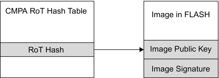
This is a vitally important hardware-based mechanism to establish an immutable RoT and is an intrinsic function of the microcontroller. We will have a closer look at how this works a bit later in this chapter. Finally, this region also contains fields to remap a (shadow) region of FLASH memory over the device reset vector.
Customer field programmable area (CFPA)
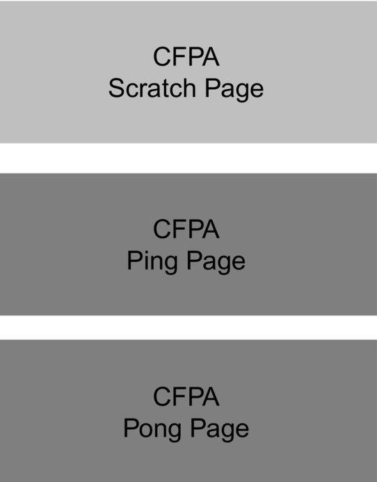
The CFPA is intended to update the CPMA settings as required during the device lifetime. In order to minimize the chance of the data being corrupted as it is modified, the CFPA data are duplicated on two pages (ping and pong) plus an additional scratch page. Each page has a version field, and when the device boots, the ROM code will use the values from the page with the highest version number. When the application needs to update the CFPA data, the new values are first written to the scratch page, and a higher version number is assigned. When the device boots, the buffered version will be written to the CFPA page with the lowest version number so that it becomes the active page (Fig. 11.7).
The CFPA has three counters, which are used to store image version numbers. These counters are monotonic (increment only) to prevent an attacker from attempting to roll back an execution image by using an old firmware update. When an update is presented, it is first validated, and then the version number is checked against the version counter. The new firmware must have a version equal to or later than the counter version in order for it to be installed. When a new version with a higher version number is installed, the counter is incremented to be equal to the latest version. This prevents an attempt to downgrade the firmware to an earlier version that may have known vulnerabilities.
The CFPA contains a second key hash table, which is used as a revocation table for currently installed keys. This functions in the same way as the RoT hash table in the CMPA but is used to hold the hash of a key that is to no longer be used. The final entry in the CFPA is a set of initialization vectors for the PRINCE run-time image encryption/decryption algorithm.
NXP programmed area
The factory programmed area contains a Universally Unique Identifier (UUID). This is a 128-bit number. There is an additional security peripheral called the Device Identifier Composite Engine (DICE), which can be used to combine the UUID with a further key to produce an identity string defined by the Trusted Computing Group. However, at the time of writing, the DICE peripheral is not supported by NXP for broad market adoption.
Key storage
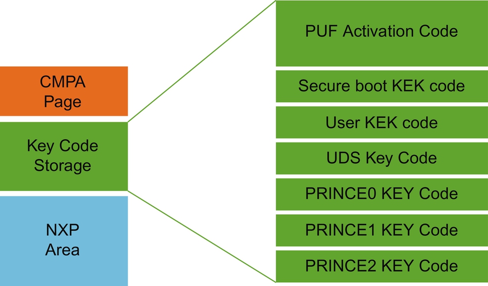
One of the major difficulties in using a “plain old microcontroller” as an IoT device is being able to store secrets such as encryption keys within the device securely. These secrets have to be held in nonvolatile memory, which will be general-purpose FLASH or EEPROM. Hence, they are at risk of being exposed through a software attack or device tampering. With the new generation of Cortex-M33 microcontrollers, silicon vendors have addressed this issue by adding Keystore peripherals to provide secure storage for encryption keys. The LPC55S69 Keystore does not hold encryption keys directly. Instead, it uses keycodes that are used to regenerate a specific encryption key using a peripheral called the Physically Unclonable Function (PUF). While it is possible to regenerate user keys by supplying a keycode to the PUF directly, the Keystore storage slots are designed to hold keycodes that are used for specific security functions. There are specific slots for the secure boot ROM, a user Key of Keys (KEK), a Unique Device Secret (UDS), and slots for each PRINCE encryption region, as shown in Fig. 11.8.
Physically unclonable function
Developed by Intrinsic ID, the Physically Unclonable Function (PUF) removes the need to store any secret keys within the device. The PUF works by combining a digital fingerprint, which is unique to the device, with a keycode to derive a unique encryption key. This key may then be regenerated after a reboot by using the same key code and the device digital fingerprint. The digital fingerprint is derived from the values held in an uninitialized SRAM. These values are random on a given device, but they are deterministic in that the SRAM will always have the same values after reset. For the purposes of this chapter, we can call this a Deterministic Uninitialized SRAM (DU SRAM). Once the power is removed, the DU SRAM data disappears, so no secret values are permanently stored on the device. This prevents retrieval of stored secrets through tampering attacks such as microprobing.
To use the PUF, we first must perform an enrolment process to generate a unique device fingerprint. Each time the enrolment process is started, it will create a new and different digital fingerprint. During the enrolment process, an activation code (AC) is output from the PUF. The device needs to be enrolled once to generate the AC, which is then used to initialize the PUF in all future sessions. During initialization, the AC is combined with the values in the DU SRAM to recreate the digital fingerprint. Second, it provides error correction codes to manage any degradation in the DU SRAM over time. When the secure boot is enabled, an AC must be stored at the start of the protected FLASH key store along with a secure boot key code. Once the PUF has been enrolled and initialized, we can create encryption keys. A new key is created within the PUF through a random process, and a unique key code will be output from the PUF. This key code acts as a handle that can then be used to regenerate the same key after the PUF has been reset. A get key function can then use the key code to read the stored key from the PUF. If we have an existing key, it can be registered with the PUF and its keycode generated. Then, the key can be regenerated using its keycode in the same fashion as PUF generated keys.
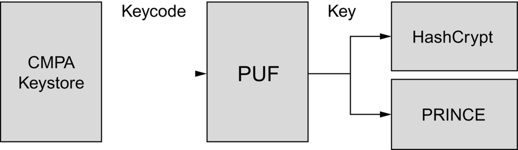
While we can use the keycodes to read out a key registered with the PUF, the LPC55S69 also contains a hardware accelerator for the AES and SHA algorithms called HashCrypt. It is possible to supply a key to this unit directly from the PUF using a local bus that is not visible to the CPU, as shown in Fig. 11.9. This creates an encryption subsystem where a secure function such as the secure boot can access a key code stored in the CMPA to reconstruct a key registered in the PUF and send the key directly to the HashCrypt encryption unit.
The PUF is controlled through a set of memory mapped registers; a subset of the critical registers is shown in Table 11.2.
| Register | Description |
|---|---|
| CTRL | Control register |
| KEYINDEX | Key index register |
| KEYSIZE | Key size register |
| KEYINPUT | User key input register |
| CODEINPUT | Code input register |
| CODEOUTPUT | Code output register |
| KEYOUTINDEX | Output index register |
| KEYOUTPUT | Key output register |
The keycode format is shown in Fig. 11.10. The key code contains fields for the registered keys size and storage index (0–15). All the index slots work the same way, except any key that is stored with index zero will be sent to either the HashCrypt or PRINCE hardware encryption units through a dedicated hardware bus that is not visible to the processor.

The type field is set to “0” for a randomly generated key and “1” for a stored user key.
Each PUF operation is controlled by writing a command code to the control register. Data transfers are managed through the CODEINPUT and CODEOUTPUT registers. The LPC55S69 provides a support library for the PUF, which includes the functions shown in Table 11.3.
| Command | Parameters | Description |
|---|---|---|
| PUF_Init() | PUF Base Address | Enables the PUF and waits until the block initializes |
| PUF_Enroll() | Base Address, [out]activation code | Performs an Enroll operation and returns an activation code |
| PUF_Start() | Base Address, activation code, activation code size | Starts the PUF with the generated activation code |
| PUF_SetIntrinsicKey() | Base Address, key index, key size, [out] key code, [out] key code size | Generates a random key and returns a key code to reconstruct the key |
| PUF_SetUserKey() | Base Address, key index, user key, user key size,[out] key code,[out] key code size | Accepts a user key and returns a key code to reconstruct the key |
| PUF_GetKey() | Base Address, key code, key code size, [out] key, [out] key size | Reconstruct a key from a key code and returns it to the user |
| PUF_GetHwKey() | Base Address, key code, key code size, key slot, key mask | Reconstruct a key from a key code and send to Hash Crypt via local bus |
| PUF_Zeroize() | Base Address | Clear all internal logic and enter error state |
| PUF_IsGetKeyAllowed() | Base Address | Checks if the get key operation is allowed |
| PUF_PowerCycle() | Base Address | Power cycles the PUF |
Before we can start using the PUF, we first need to perform an enroll process to generate an activation code by writing the PUF_ENROLL command to the CODEINPUT register (Fig. 11.11).

When the enroll is completed, the activation code can be read from the PUF CODEOUTPUT register. The activation code is 1192 bytes in size, and it can be stored in any nonvolatile location. The CMPA protected flash page provides a storage location for the activation code so that it can be used by the secure boot ROM at startup. Ideally, it will only be necessary to perform an enroll process once per device. Once the activation code has been generated, it is possible to disable further enroll commands by setting on OTP fuse (Fig. 11.12).
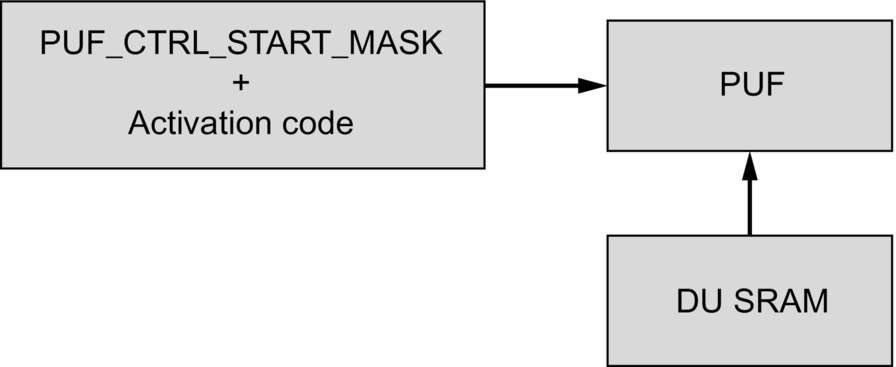
When the activation code has been generated, we can place the PUF into its operational mode by issuing a START command. During this operation, the activation code is written to the CODEINPUT register in 32-bit chunks. Once the start command has been successfully executed, we can configure the PUF to hold our encryption keys.
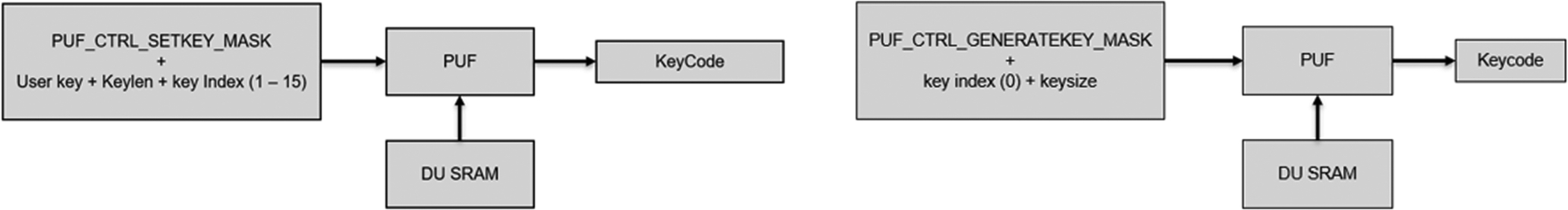
Once the PUF has been started with a valid activation code, there are two methods of registering a key. You can either use the PUF to create a random key by using the GENERATEKEY command or register an existing user key with the SETKEY command (Fig. 11.13).
In either case, the PUF will return a keycode that in combination with a PUF_CTRL_GETKEY_MASK command to retrieve the key. In the case of a key that has been stored with index zero, the key will be sent via the hardware bus to the PRINCE and HashCrypt units (Fig. 11.14).
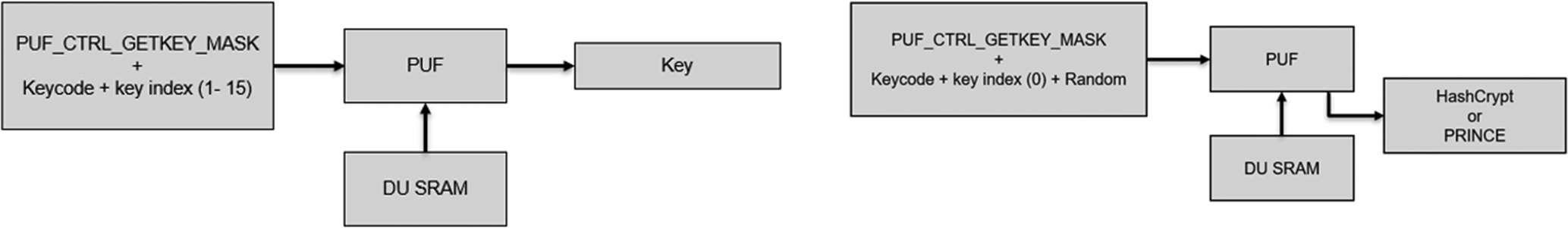
When we use a key with index zero, an additional block of random data must be passed to the PUF. This is used as “blinding” data, which masks the encryption key as it is transferred to the encryption engine. This is intended to mitigate against side-channel attacks.
Exercise: Key storage using the PUF
This exercise demonstrates how to use the PUF to “store” and generate a pair of keys. Both keys are retrieved from the PUF, and the “stored” key is tested against the original.
- In the pack installer, select Example 11.1 and press the Copy button.
- Build the project and start the debugger.
- Step through the enroll and start functions.
This will create and use the activation code.
- Now step through the key set and generate key functions.
This will “store” the user key and create a new random key and return keycodes for future access.
The key codes and activation codes are public information. They cannot be used to reconstruct the “stored” keys without access to the deterministic uninitialized SRAM values, which are both hidden and unique to each device.
- Now run the getkey function and key compare functions.
This will retrieve the “stored” key and check that it matches the original values.
Secure boot
After a reset, the LPC55S69 will execute code in the boot ROM before passing execution to the application image in the FLASH memory. The boot ROM can be configured to perform a secure boot process that validates the device images to provide an immutable RoT. The LPC55S69 secure boot is certified as a PSA Level 1 and Level 2 device. The secure boot process is a critical part of the Arm Platform Security Architecture that is used to establish an initial RoT that all future device security is based on.
The LPC55S69 is designed to support a standard plain boot which will automatically execute any image that is programmed into the internal FLASH memory. This is used during development when it is necessary to update the execution image frequently. The LPC55S69 also supports a boot process that validates the execution image using a CRC32 checksum. While this is a useful self-test measurement, it only provides a weak (in cryptographic terms) measure of image integrity and does nothing to authenticate the image. This would leave our device wide open to rogue images and potential malware. We need something stronger.
For our uses, the LPC55S69 has both hardware support and ROMed system code for a sophisticated secure boot process. While this is specific to this family of devices, understanding how it works provides a useful introduction to the implementation of the of the PSA secure boot requirements.
The LPC55S69 secure boot performs the following functions:
- • Validation of the FLASH memory images before starting execution.
- • Configure and enable the TrustZone SAU.
- • Perform an In System Programming (ISP) software update over a range of serial interfaces, such as USART SPI or USB.
The ROM also provides an API to the application code so we can access its functions to perform In-Application Programming (IAP) via a second-stage bootloader.
When the secure boot is enabled, the FLASH image must be formatted is shown in Fig. 11.15.
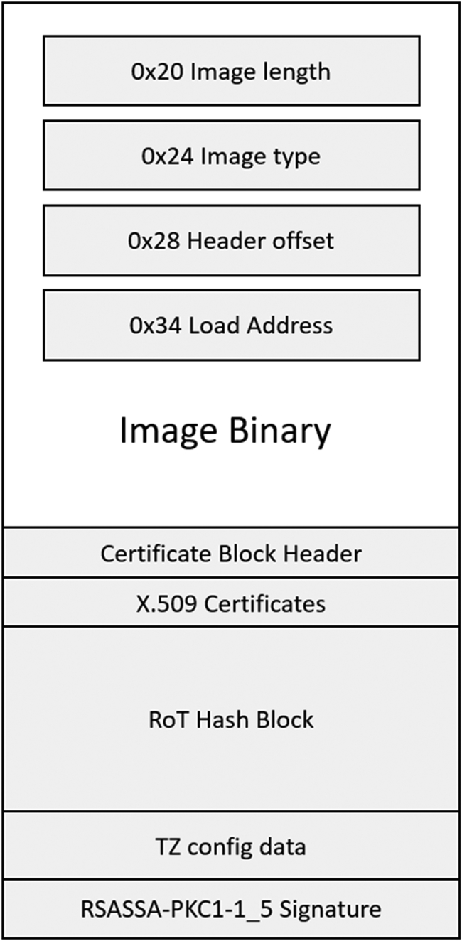
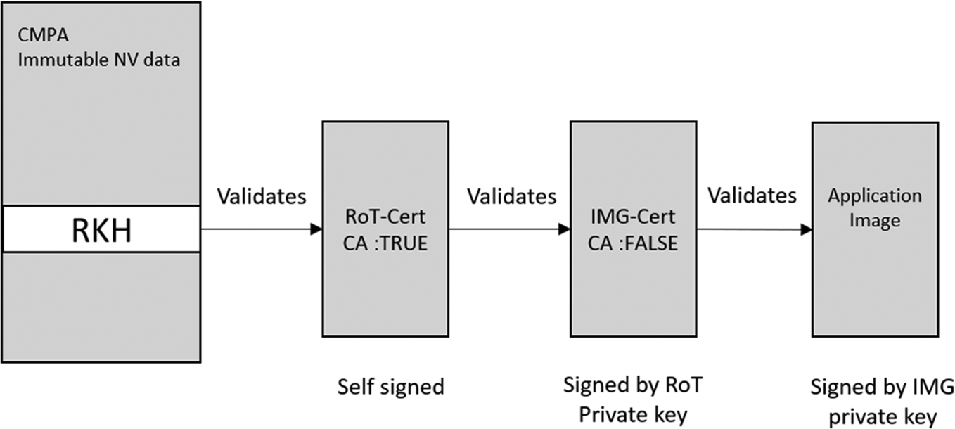
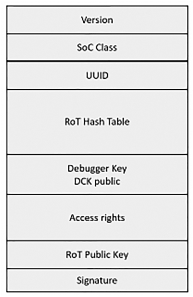
In addition to the binary application code, the image contains a block of security credentials. These consist of an X.509 certificate block and a set of RoT key hashes followed by TrustZone configuration information. The code image and security block are signed by the private half of an RSA (2048) key pair. This is called the Image-Signing Key (IPK). Typically, the security credentials will be appended to the end of the code image but can be located anywhere within the signed region. The address of the security header block is stored in the exception vector table and occupies the reserved (unused) vector at 0x 00000024. This allows the secure bootloader to locate the security credentials and validate the FLASH image.
The security credentials start with a block of X.509 certificates. While this block is capable of holding a chain of up to sixteen certificates, the most common configuration uses two certificates. The first certificate is a self-signed root certificate that contains a Root Public Key (RPK), which is used as a Certificate Authority (CA). The second certificate contains the Image Signing Public Key (IPK) and is signed by the private half of the RPK. In order to anchor the certificates to the LPC55S69, a Hash of the RPK is stored in the CPMA page of the protected FLASH. Once the CPMA page has been programmed, it can be sealed, which makes its contents immutable. This gives us an immutable RoT hash value, which is used by the secure boot loader to validate the public key stored in the root certificate. The root certificate is then used to extend the chain of trust by validating the image signing certificate IPK. If this is successful, the IPK public key can be used to validate the full image signature. The full Chain of Trust is shown in Fig. 11.16.
So why use two certificates? It is possible to use a single certificate and use its key to validate the image. However, this certificate is bound to the device through the Immutable Root Key Hash Table. If its matching private key is compromised, we have no way of updating the public certificate and hash value. By using two certificates, we are creating an additional “bastion” layer of security that future-proofs our devices against such a compromise. In this approach, the root certificate private key will be used as little as possible and stored away very securely. Typically, the RPK private key is used just once to sign the Image Signing Certificate (IPK). Now all update images will be signed by the IPK private key. This means we make regular use of the IPK private key, potentially making it more liable to be compromised to an unauthorized third party. If this does happen, we can create a new IPK signing key pair and a fresh X.509 image certificate, which will again be signed by the RPK private key since this is still valid.
All new images will be signed with the fresh Image Signing Key (IPK private), and the image will be encapsulated with the original RPK and the new IPK certificates. This allows us to recover from the compromise without having to modify the RoT hash in our devices. As mentioned earlier, a hash of the RKP public key is stored in the CMPA block protected flash area. Since this is immutable once programmed, it would be a big problem if the RKP private key was compromised. We would have no easy way to make our devices trust a different key. In order to minimize this threat, the CMPA block has a RoT hash table that can store up to four RPK public key hashes (Fig. 11.17).

This allows us to pre-generate up to four RPK key pairs and store their hashes in our devices when they are manufactured. The first key in the table will automatically be the active key, and the remainder are stored for possible future use. If we need to switch to a new Root Key, the Protected Flash CFPA block provides a mechanism to revoke the existing RoT key hash and activate the next entry in the table. This can be done up to four times (to lose one private key…). The hash table is further protected by a root key table hash (RKTH), which is a hash of the hash table.
Monotonic counters
To prevent an attacker from installing an unauthorized or older version of the device firmware, the Protected flash CFPA page contains three monotonic counters (they can be incremented but not decremented). These counters are used for firmware version control and revocation of the secure boot certificate keys.
If the IPK private key has been compromised, it would be possible for an attacker to create their own image and sign it with the compromised IPK. The CFPA provides a counter that is used to store the serial number of the Image Signing Certificate. For the image update to be accepted, the serial number must either match or be one count higher than the current counter value. The counter is restricted to a range of seventeen set values, which effectively restrict the range of the IPK certificate serial number.
The first two counters are used to store the current Secure firmware version and the current nonsecure firmware version. When a new image is installed the version, numbers stored in the update image must be the same or later than the value stored in the hardware counters. If this is not the case, the firmware will be rejected. This is intended to prevent an attacker from rolling back the firmware to an earlier version with known vulnerabilities.
Once enabled, the secure boot ROM within the LPC55S69 is always the first code to execute after reset. The secure boot ROM will validate an initial image located within the FLASH memory. In terms of our security model, this will be the updatable Root of Trust, which is the second stage bootloader BL2. If this image is successfully validated, the boot ROM will pass execution to the BL2 image. The BL2 bootloader will, in turn, validate the remaining secure code image and the nonsecure image before passing execution to the secure application code. We will have a look at the BL2 bootloader in Chapter 14.
Exercise: Secure boot
NXP has made the process of creating the necessary credentials and secure boot image very straight forward, with an easy to use an application called “MCU Expresso Secure provisioning.” This tool can be downloaded from their website to provide a self-contained environment that automates the entire provisioning process.
- However, before we look at this tool, it is important to note that it will fully enable the secure boot support, which cannot be reversed. This tool should only be used to program a device where you want the boot security permanently enabled.
You can download the secure provisioning tool from the following URL:
Start the tool and select the LPC55Sxx as the target device.
First select the Key management tab.
Press the Generate Key tab (Fig. 11.18).
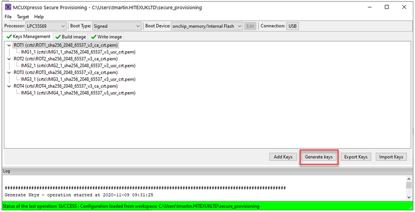
This will generate four sets of RoT certificates and associated image signing certificates along with their private keys. It will also generate a symmetrical Secure Binary Encryption Key SBKEK, which is used to encrypt the binary update image. During provisioning, the SBKEK key is stored in the CMFA.
Next, select the build image tab. Here we need to provide the raw binary file and a name for the output secure boot image. The start address for the image is zero. In this example, we are not going to use the secure boot ROM to configure TrustZone, so this is disabled. Finally, we can select the Root of Trust Hash that will be used to anchor the certificate chain. Once these options are set, press the build image button, and the tools will generate the bootable image and the provisioning credentials for the protected FLASH CMPA page (Fig. 11.19).

Once the image has been generated, we can use the provisioning tool to download it into the device.
- This is the bit you should not do unless you want to permanently enable the secure boot! (Fig. 11.20).

Fig. 11.20 Secure Boot Warning. Do not proceed beyond this screen unless you want to permanently enable secure boot! No permission required.
- Connect a USB cable to the Xpresso P9 USB port.
- Place the board into its bootloader mode by holding down the ISP button and pressing Reset.
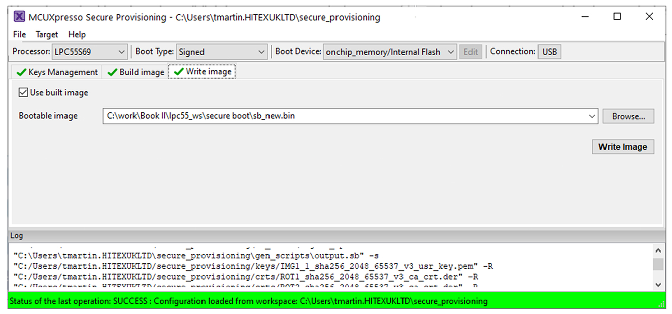
- Now press the Write Image button.
This will download the secure boot image into the internal flash and program the CMPA page. It will also seal the device by setting the CMPA Hash value (Fig. 11.21).
Once the board is reset, the secure boot process will be active. Any updated application image must be correctly encapsulated and signed before it will be accepted by the microcontroller.
Debug authentication
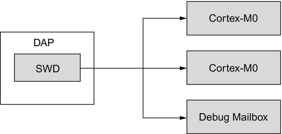
The LPC55S69 extends the Cortex-M33 processor debug authentication to enable tiered debug access in a final product. The debug architecture provides debug access points for each Cortex-M33 core plus a debug mailbox, which is used by the debugger to negotiate a secure debug session (Fig. 11.22).
When the debug security is configured, the debug mailbox remains enabled, while both of the core debug access points are disabled. When a debugger wants to connect, it must go through a challenge-response messaging protocol using the debug mailbox.
To configure the LPC55S69 debug authentication, an asymmetric key pair must be generated to act as the Root of Trust. The public key is then stored in the device along with a set of credentials that define different types of debug access. Different users are granted access through a debug credential certificate. To create this certificate, the user must generate a second public key pair. The public key is given to the OEM vendor, and this is placed into the certificate along with the credential constraints appropriate to the access he requires. The certificate may also include a UUID field which, limits the certificate to activate a specific device. This binds together the end user’s identity and access rights (Fig. 11.23).
To start a debug session, the technician connects to the debug mailbox, and the device will send a debug authentication challenge. This contains the stored credential constraints and some random data. The debugger must now have a matching debug credential that will allow it to negotiate its authorized level of debug access. In order to reply, the debugger then generates a response packet which includes its debug credential certificate and the random data. The random data act as a nonce to prevent replay attacks. If the authentication is successful, the device will enable the debug ports, and grant access appropriate to the certificate credentials (Fig. 11.24).

Lifecycle
This system allows us to implement the PSA lifecycle model for debug access. During manufacture, the device will be open for assembly and test. When it is programmed with the application firmware, the device can also be provisioned with secrets, including the debug private key and the credential constraints. At this point, the device can enter its active state with secure boot enabled, and the debug port will be locked down.
As part of the service contract, the vendor can create a range of the third-party debug credential certificates that allow debug access to the nonsecure code and OEM debug credential certificates to allow full access for vendor technicians.
Hardware accelerators
The LPC55S69 has three cryptographic hardware accelerators: HashCrypt, which provides symmetric encryption and hash algorithms, CASPER, which supports rapid calculation of asymmetric algorithms and PRINCE, which is able to support execution of encrypted images with a zero cycle overhead (Table 11.4).
| Function | Algorithms | Accelerator |
|---|---|---|
| Symmetric Cipher | AES (ECB, CBC,CTR) PRINCE (CTR) | Hash Crypt 128,192 & 256 bit keys |
| Asymmetric Cipher | RSA, ECC | CASPER |
| Hash | SHA-1, SHA-256 | HASH Crypt |
| MAC | HMAC, CMAC | HashCrypt + Software |
| Signature | RSA, ECDSA | HashCrypt and CASPER |
Asymmetric encryption
The CASPER hardware unit supports hardware calculation of the RSA asymmetric encryption algorithm, the Diffe Hellman Key Agreement algorithm, and Elliptic Curve Cryptography, including the Elliptic Curve Digital Signature Algorithm. In order to reach a high level of security, each of these algorithms uses very large numbers. While arithmetic with these numbers can be done in software using the mbedTLS Bignum library, it is both computationally intensive and energy-hungry. Being able to offload these calculations into a hardware co-processor has clear advantages.
The CASPER unit is a general-purpose computational engine. The acronym stands for Cryptographic Accelerator and Signaling Processing Engine with RAM sharing. While it is primarily intended for cryptographic use, the CASPER coprocessor can be programmed to perform a wide range of mathematical algorithms such as DSP algorithms, matrix math, and even graphics acceleration such as shading.
The CASPER coprocessor takes its input from four RAM banks that can be accessed simultaneously, allowing the CASPER coprocessor to load 128 bits of data in a single cycle. The coprocessor has several layers of computational blocks. The first layer provides two 32 bit multipliers that can multiply various combinations of the input words to give a 64- or 32-bit intermediate result. These results may either be carried through to the final output layer, or a half word from each intermediate result may be combined in an adder unit. In this case, the lower half word from one intermediate result and the upper half word from the second intermediate result are used. The final output layer consists of four results blocks that can load the intermediate results via a multiplexer (Fig. 11.25).
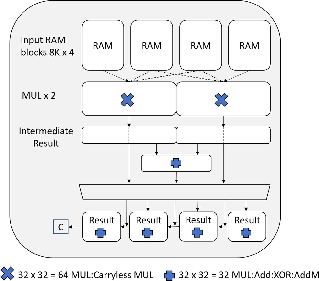
Each of the results blocks contains an adder unit and results register which operate in parallel. There are several different data paths for each results block that can be individually configured. This array of hardware arithmetic units and multiplexers allows us to perform complex calculations, store constants, and use data from the previous calculation.
The CASPER coprocessor is programmed as a state machine with each calculation step programmed by a mode command. Fortunately, a number of low-level cryptographic primitives are provided for the CASPER coprocessor, so unless you need to implement a custom algorithm, it is unlikely you will need to program it directly.
Exercise: Casper primitives
- In the pack installer, select Example 11.2 and press the Copy button.
- Build the project and download to the debugger.
The code will use the CASPER unit to perform modular exponentiation. The code is annotated with debugger event recorder macros, which are used to display the execution time:
CASPER_ModExp(CASPER, (void *)signature0, (void *)pubkey0, sizeof(plaintext0) / sizeof(uint32_t), pub_e, plaintext);
- Set a breakpoint after the casper_modEXP function.
Run the code and note the execution time in the viewevent statistics window.
The code will next perform elliptic curve scalar multiplication, which has also been annotated with event recorder macros.
- Set a further breakpoint at the end of the code and note the timing measurements in the event statistics window.
The mbedTLS library has been ported to use the CASPER coprocessor for the asymmetric algorithms. The table below shows the performance boost for each of the supported algorithms (Table 11.5).
| Algorithm | Operation | SW execution time (mS) | CASPER execution time (mS) | Improvement % |
|---|---|---|---|---|
| Signing | ECDSA—secp256r1 | 333.33 | 142.86 | 233 |
| Verification | ECDSA—secp256r1 | 598.80 | 149.93 | 399 |
| Key Exchange | ECDSA—secp256r1 | 300.30 | 130.38 | 230 |
| Signing | RSA—1024 | 250.00 | 272.48 | − 9 |
| Verification | RSA—1024 | 8.9 | 1.81 | 493 |
| Signing | RSA—2048 | 1000.00 | 1000.00 | 0 |
| Verification | RSA—2048 | 31.92 | 5.03 | 635 |
Symmetric cryptography
The LPC55S69 provides a second dedicated cryptography processor for the key symmetric cryptography algorithms. The HashCrypt processor provides hardware acceleration for the AES cipher and the SHA message digest algorithms. A hash or cipher based MAC can be implemented with additional software, as discussed in Chapter 4.
The HashCrypt processor provides a fixed implementation of the AES algorithm and supports encryption key sizes of 128, 192, 256 bits. The user software may provide the encryption keys in the case of session keys, or as we saw earlier, a key may be provided from the PUF key store. In this case, the key will be sent to the HashCrypt unit via a local bus which is not observed by the CPU. While the AES supports ECB mode, it also supports various streaming modes, including CBC and CTR modes. The HashCrypt processor provides an additional streaming mode called IBC, which is designed to prevent side-channel analysis and is intended to protect data at rest rather than communications data. Once configured encryption/decryption operations will take 32 + 2 cycles per AES block.
As its name implies, the HashCrypt processor also provides a hashing or message digest function using the SHA-1 and SHA-2 algorithms. The HASHING function will process blocks of 512 bytes at a time for the SHA-1 algorithm. This will take 80 cycles while the SHA-2 takes only 64 cycles, which is much faster than a software implementation. To further speed things up, the data blocks can be provided by internal DMA transfers from memory or peripheral buffers.
Exercise: HashCrypt
In this exercise, we will use the HashCrypt peripheral to encrypt and decrypt data using the AES cipher and its chaining modes. The code uses both a user-supplied key and a key that is securely stored in the PUF unit. The project then uses the HashCrypt peripheral to generate SHA1 and SHA256 hashes.
- In the pack installer, select Example 11.3 and press the Copy button.
- Examine the code in the HashCrypt.c file.
The first section of the code provides functions that test the AES engine in Electronic Code Book format and chained modes CBC and CTR with a user-supplied key.
The second section uses an encryption key stored in the PUF using index zero, so it is delivered through the dedicated hardware bus. This ensures that no secret key is held on the device, and during operation, the reconstructed key is never visible to the CPU.
The final section is used to generate SHA1 and SHA256 hashes.
- Build the project and Start the debugger.
- Run the code and check the output messages in the console window.
Executable image encryption
The final cryptographic co-processor is used to encrypt and decrypt the firmware image using a lightweight symmetrical block cipher called PRINCE. However, while the PRINCE algorithm is a proprietary algorithm it has been subjected to extensive cryptoanalysis and was selected through a challenge competition. The cipher itself is used to encrypt/decrypt 64-bit blocks of data using a 128-bit key. Interestingly, the program images do not need to be encrypted before being downloaded into the microcontroller. Once image encryption is enabled, the PRINCE cipher will automatically encrypt image data as it is programmed into the FLASH memory. Then during normal execution, each instruction will be decrypted on the fly with zero overhead beyond the standard FLASH access time.
The program FLASH memory is divided into three sections, two of 256 K and a final section of 128 K. Each section has a separate encryption key, which are each stored in the PUF. The CMPA has dedicated storage slots for the resulting PUF keycodes, which are accessed by the PRINCE unit when image encryption is enabled.
Exercise: Image encryption
In this exercise, we will first provision the CMPA with keys for the three PRINCE regions and then download an image using the ISP programming support. This will allow the PRINCE engine to encrypt the image as it is downloaded. We can then check that the image executes successfully and view the encrypted code using the debugger assembler view.
- Warning: Like the secure boot example, this exercise is for information only. Once you have set the encryption options, your device will automatically encrypt the code that is downloaded via the bootloader.
- Install the J10 jumper to allow the ISP mode after the reset.
- Connect a micro USB cable between the PC host and the CMSIS DAP USB port (P6) on the board.
- Open the Command Prompt, move to the folder with the blhost.exe and apply the following commands:
blhost -p comX -- key-provisioning enroll blhost -p comX -- key-provisioning set_key 7 16 blhost -p comX -- key-provisioning set_key 8 16 blhost -p comX -- key-provisioning set_key 9 16 blhost -p comX -- key-provisioning write_key_nonvolatile 0
- Remove the J10 jumper and reset the board.
- Open a serial terminal with the following settings 15200 8N1.
- Download the program to the target board.
- Either press the reset button on your board.
- Once you have seen the code execute correctly start the debugger.
- Open the viewassembly window.
- Run the code to main().
- Examine the code in the assembly window.
Security peripherals
Entropy source
As we saw in the cryptography chapters, the generation of secret keys should be done through a random process. Random numbers are also used during the TLS handshake. This makes a cryptographically strong RNG as important to our overall security as the secrecy of our encryption keys. Like most microcontrollers designed for IoT use, the LPC55S69 has a True Random Number Generator (TRNG) with 256 bits of entropy (uncertainty). The TRNG is certified to meet and exceed current standards such as FIPS140–2, AIS31, and P2/PTG.3.
Secure user peripherals
The security control block contains a number of additional registers to manage other security concerns within the LPC55S69. While controlling memory access is a driving concern, other signals such as interrupt channels also cross the boundary between secure and nonsecure code. We need to ensure that useful information does not leak from the Secure world. Within the Security Control Block, we can also lock some important processor configuration options so that an attacker cannot modify them while the device is running.
Secure interrupt masking
The LPC55S69 contains two Cortex-M33 CPU’s but only CPU-0 is fitted with TrustZone. The memory and peripheral access rights for CPU-1 are defined by a Master Security Wrapper in the same fashion as the other bus masters. However, all of the peripheral interrupts are also routed to the NVIC in CPU-1. If CPU-1 is being used to execute nonsecure code, it is still able to see interrupt activity from the secure peripherals. To close this loophole, the Security Control Module provides a set of masking registers that can be used to disable the connection of selected peripheral interrupts to the NVIC in CPU-1.
Secure DMA unit
The LPC55S69 has two general-purpose DMA units with multiple independent channels. After reset, either DMA unit may be accessed by each of the Cortex-M33 processors. To prevent this from becoming a security risk, one unit can be assigned to the nonsecure code, while the second is used by the secure code by defining its access rights using its Master Security Wrapper. However, all of the peripheral interrupt signals are routed to both DMA units so they can act as flow controllers. This could potentially expose some secure information to the nonsecure DMA unit. To prevent this from becoming a problem once a DMA unit is assigned to the secure code, a set of masking registers can be used to prevent DMA requests from secure peripherals from being routed to the nonsecure DMA unit.
GPIO masking
On LPC55S69, all digital pins states are readable through GPIO controller registers, which means that information can leak through pins connected to peripherals configured as a secure peripheral.
On the LPC55S69, any digital I/O that is sensitive to information leakage can be masked using SEC_GPIO_MASK0/1/2/3 registers to ensure that the nonsecure code cannot snoop on the activity of secure peripherals.
Secure GPIO
The LPC55S69 provides a secondary set of GPIO registers for GPIO port 0.
The security control block provides a pair of registers than are used to lock access to processor configuration options within CPU-0 and CPU-1.
The CPU-0 and CPU-1 lock registers contain bit fields that, when set, prohibit further configuration of each processor. Each lock register also contains a bit that, when set, locks the register itself from further updates until a device reset is performed.
Conclusion
In this chapter, we have seen how a Cortex-M33 based microcontroller can build on the TrustZone security extension to create a run time trusted execution environment. Typical microcontrollers designed to be the basis of an IoT device will also provide a PSA-certified secure boot process that is held in immutable ROM. The silicon vendor should also provide a region of memory that can be programmed with key device information when the device is manufactured. The device must also have a strong source of entropy in the form of a true random number generator. Ideally, the microcontroller will also have a set of monotonic counters for image versioning. Beyond these base features, the device is likely to provide a range of security assistive peripherals such as a secure key store and cryptographic accelerators. Once you have a device that meets all these requirements, you can start thinking about the application.