
Library modeling
Abstract
Keywords
component
library
cell model
specify block
user-defined primitive
timing checks
Once a design has been verified, the next step is logic synthesis. Logic synthesis produces a technology-dependent netlist implementation of the design. Such a netlist needs to include instances of cell models. All the cell models for a given target technology are gathered together into a library. This chapter deals with creating cell models for a component library.
Component libraries
The synthesizer will reference a library of components to map the design into the target technology. This library will typically contain hundreds of Boolean logic gates, complex cells, and flipflops. There may be numerous cells that are logically identical but have different speed and power characteristics.
Because gate-level simulation with annotated timing information is slow, designers may depend on timing reports generated by the logic synthesizer or other static timing analysis tools to ensure that the implementation meets all performance requirements, but simulating the netlist with the verification suite already developed often finds obscure timing problems not caught by static timing analysis. Before any such simulation can be done, a Verilog component library is needed. A component library is a link between an abstract behavioral design and the ultimate goal, a physical implementation.
Libraries have a cell model for each component. They will have to be updated for each new semiconductor process, even if no cells are added or subtracted from the library, as the performance characteristics of the cells will have changed.
An example of behavioral code for a four-bit counter and the synthesized netlist produced from it is shown in Figure 11.1. In this example, the Synopsys®, Inc. 90 nm SAED Generic Library [1] was targeted and the Synopsys Design Compiler tool was used for synthesis. This library is made available from Synopsys to universities for educational purposes and requires an educational addendum to the normal tool license [2].

In order to simulate the gate-level implementation, Verilog modules for the flipflops (cell DFFARX1) and each of the combinational gates would be needed. All the models for a given technology would be gathered together in one library. Some libraries have all cells in a single Verilog file and others have a separate file for each component, with the library then consisting of the directory where all the files are stored. The Synopsys library used in this example has all the cells in a single file.
Cell models
Each cell model has both behavioral and timing data. For combinational cells, timing data are limited to propagation paths from inputs to outputs. Sequential cells also need timing checks to ensure that operating parameters such as setup and hold times are not violated.
In the simplest case, a cell model can have a single delay parameter added to the instantiation of a primitive component. Delay parameters can also be separated into rise times and fall times for more accurate modeling. Examples of such models are shown in Figure 11.2. This type of modeling is rarely used in modern libraries for timing simulation but can be found when only functional verification is being used. In Figure 11.2, the timescale directive at the top will be used for both modules. Having only a single timescale directive at the top of a file containing many library models is standard procedure.

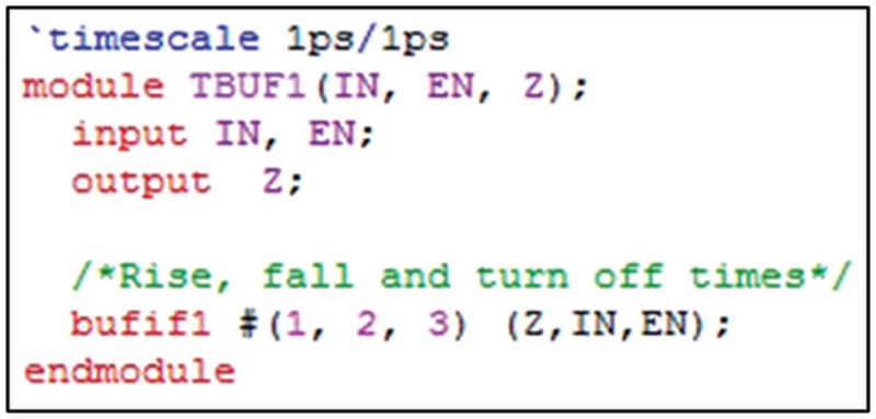
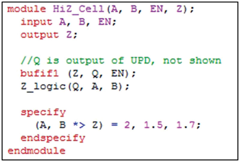
A third field for turn-off time can be added for cells that have the capability of being put into a high-impedance state. Figure 11.3 shows a Tri-state® buffer cell that has a zero-to-one transition time of 1 ps, a one-to-zero transition time of 2 ps, and a turn-off time of 3 ps. With this type of delay modeling, the high impedance to zero time is the same as the one-to-zero time and the high impedance to one time is the same as the zero-to-one time.
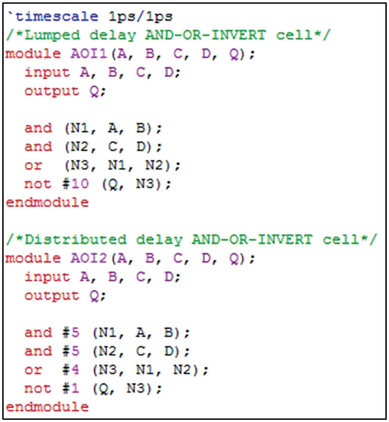
A model of a more complex cell, such as an AND-OR-INVERT function, could have all the delay lumped together on the output driver or it could be distributed among the primitive operations. Both methods are shown in Figure 11.4. The two AND gates in each cell are in parallel, so the input-to-output delays of cells AOI1 and AOI2 are identical. The simple lumped delay model assumes all input to output paths have the same delay, which will not always be the case.
Paths from inputs to outputs can, as has been shown in Figure 11.3, have different delay characteristics for rise, fall, and turn-off times. In addition to these differences, semiconductors will not always perform the same under all operating conditions. Temperature, power supply, and manufacturing variability will affect the speed at which an electronic component can operate. Taken together, these three define a performance envelope for a component.
Each device will have a nominal operating voltage. However, it would be impractical to specify the voltage to infinite precision. Instead, a range is specified. For old TTL components, the supply voltage is 5 V, plus or minus a quarter of a Volt. More modern technologies use lower values but still have a range of acceptable voltage. Even if the supply voltage happens to be the nominal value to a thousand decimal places when the circuit is in its quiescent state, it will fluctuate with circuit switching, so some tolerance in the power supply is always needed.
Although circuits must continue to work as long as the power supply is within the specified range, they do not operate at exactly the same speed across the entire range of acceptable supply voltages. Operating speed decreases with reduced voltage.
Each device will also have a specified temperature range. Commercial components are normally specified to operate between 0 °C and 70 °C. Military grade components need to operate over a larger range, from −55 °C to +125 °C. As with supply voltage, delay characteristics will fluctuate with temperature. CMOS components tend to be linear with temperature for both rise and fall times, operating faster as the temperature drops. In TTL devices, fall times decrease with rising temperatures while rise times increase, but TTL is not used in modern integrated circuits.
In addition to these external variables, there will be some fluctuations in the delay characteristics of the devices produced when supply voltage and temperature are held constant. There are dozens of different factors that affect delays in semiconductors, but all can be lumped together to form a single “process” variable. Testing should weed out the devices that fail to meet specified delay characteristics, but there will remain some range of operating speeds for the devices that are deemed acceptable.
Process, temperature, and voltage can be combined to form scaling factors. When all three are optimal, the device will operate “best case.” When all three are at their worst, a “worst case” scaling factor is applied to delays. Nominal delay values will form the “typical case” setting.
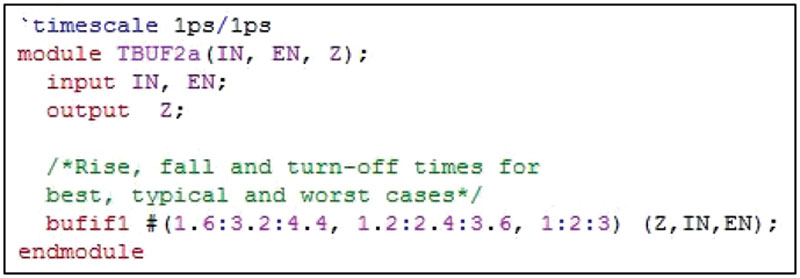
A semiconductor vendor may choose to provide separate libraries for each case or may have all in one library, with the delays multiplied by a scaling factor depending on which operating condition is chosen. When best, typical, and worst case delays are all in the same library, the rise, fall, and turn-off times of each cell are replaced by triplets for each field in the format Min:Typ:Max. Thus for a Tri-state cell, there will be three triplets, representing minimum, typical, and maximum delays for rise, fall, and turn-off times. Cells without Tri-state capability will only have two triplets, one for rise times and the other for fall times.
An example of a Tri-state buffer cell with three operating conditions is shown in Figure 11.5. When simulating worst-case conditions, the zero-to-one transition time will be 4.4 ps. For best case, the one-to-zero time will be 1.2 ps and for the typical case, the turn-off time will be 2 ps.
The distributed delay model offers the option of having some different paths through a cell, but its flexibility is still too limited for accurate timing simulation. Specify blocks are used to enumerate pin-to-pin delays across a cell.
The Tri-state buffer cell shown in Figure 11.5 has been modified in Figure 11.6 to use a specify block for timing data. Because that cell has only one data path from input to output, there is no obvious advantage to putting the delay information into a specify block, but not all cells are so simple.

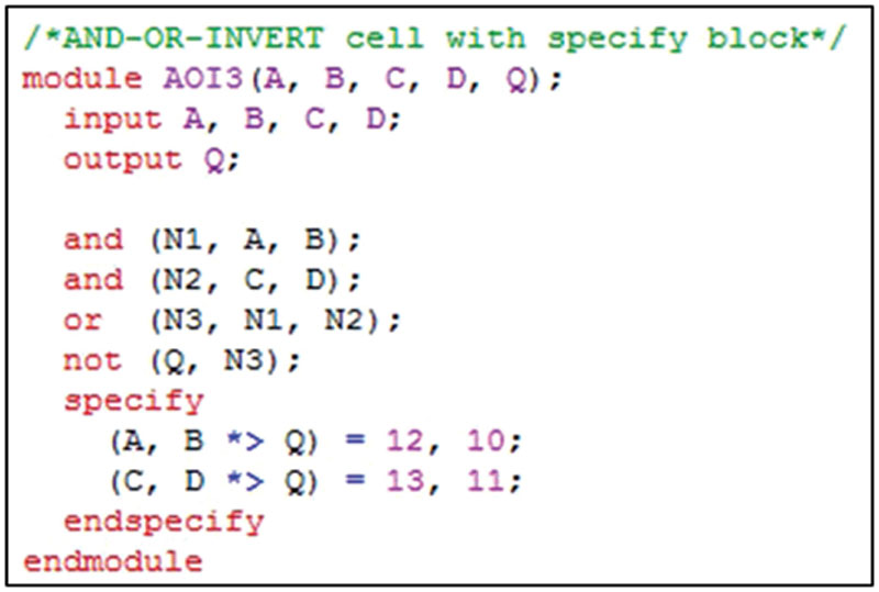
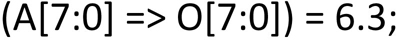
In Figure 11.7, the AND-OR-INVERT cell first introduced in Figure 11.4 is shown with two different path delays from inputs to outputs. Use of the full connector operator *> indicates that both the path from A and the path from B have a 12 time unit rise time and a 10 time unit fall time. The full connector operator can also be applied to cells that have multiple outputs. The path specification shown below indicates that the paths from any bit of A to any bit of O will take 6.3 time units and that there are 64 total paths with the same delay characteristic.

The above path specification indicates that any bit of A may cause a transition on any bit of O. The alternative for multiple input-to-output paths is to specify each in parallel, using => for each path. The following line of code indicates that there are eight parallel paths, each having a delay of 6.3.
Just as was done with parameters and localparams, giving meaningful, mnemonic names that can be updated in one place can help make cell models easier to understand and maintain. Within specify blocks, specify parameters, or specparams are used. Like localparams, specparams are fixed and cannot be redefined at compile time.
Figure 11.8 shows a two-input AND-gate model from the Synopsys library used in Figure 11.1. This model is written to allow two modes of operation: if “functional” is defined, a simple one-unit delay is used. When full timing information is required, rise and fall times from each input to the output are available. The specify block delays will override the unit delay associated with the primitive instance. There are separate libraries for best and worst case, so only one set of delays is included in each cell model.

The cell shown in Figure 11.8 uses +=> to specify that the path from the inputs to the output is noninverting and that a zero-to-one transition on an input will result in a zero-to-one transition on the output, if there is to be any change. Use of −=> in a specify block indicates an inverting path and a zero-to-one transition on an input that causes a change on the output should use the high-to-low delay figure rather than the low-to-high transition time. Plus and minus modifiers to delay paths can be used with full connections as well as with parallel paths.
An alternative syntax for specifying inverting and noninverting paths is to add a separate field for that in the path specification. The two lines below are equivalent.
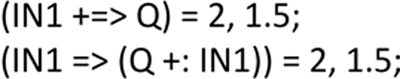
If a rising edge on IN1 would cause a high-to-low transition on Q, both of the following lines would indicate that the high-to-low transition time is to be used and a falling edge on IN1 would mean that the output delay would be that of a zero-to-one transition.

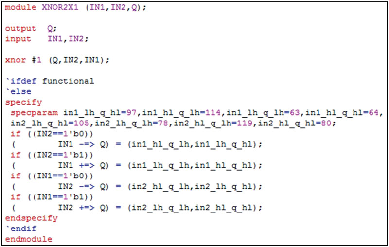
Sometimes path polarity is conditional on the state of another input. An example of this is a two-input XNOR gate. If one input is steady state zero, then a change on the other one precipitates an inverting path from it to the output. Conversely, if an input is steady state one, a change on the other input would cause the output to follow the changing input with no inversion. To allow for such run-time path variations and always associate the right delay with each transition, conditional statements may be embedded in specify blocks. Unlike standard Verilog conditional statements, only “if” clauses are allowed. Neither “else if” nor “else” may appear in a specify block. A model for such a cell is shown in Figure 11.9. It also was extracted from the Synopsys 90-nm library.
User-defined primitives
So far, all models used in these examples have had their functionality defined by the instantiation of a single built-in primitive or, in the case of the AND-OR-INVERT models, a small number of primitives. While any function can be modeled with the built-in primitives, cells that use large numbers of them will simulate slowly.
To improve simulation performance, library developers may define their own primitive functions. User-defined primitives (UDPs) have their logical behavior specified in a table. Like built-in primitives, UDPs must have exactly one output. Combinational UDPs may have up to 10 inputs. Sequential UDPs are limited to nine inputs, as they also need a value for current state.
In addition to standard zero, one, and x values, UDP tables can use several symbols to decrease the number of table entries needed to fully specify the function. UDP symbols are shown in Table 11.1. Combinational UDPs only use the first two symbols. Sequential UDPs may use all.
Table 11.1
UDP table symbols
| Symbol | Meaning |
| ? | Iteration over 0, 1, and x |
| b | Iteration over 0 and 1 |
| - | No change |
| r | Rising edge: 0 to 1 transition |
| f | Falling edge: 1 to 0 transition |
| p | Potential rising edge: 0 to 1, x to 1, or 0 to x transition |
| n | Potential falling edge: 1 to 0, x to 0, or 1 to x transition |
| * | Any transition |
Combinational cells
A full adder is a cell that could benefit from being implemented as a UDP. Since a full adder needs two outputs, two tables will be needed but this is in contrast to at least five primitive operators for a model without UDPs. Figure 11.10 shows a model for a full adder incorporating a module and two primitives.

The carryout term will be set to one whenever two out of the three inputs are one, so the third input in those cases is don’t care. Use of a question mark for such cases covers any value for the third input, allowing the table to be shorter than if all values needed to be explicitly iterated. No such optimization is possible for the sum term, so all eight input combinations are enumerated there. In a UDP table, any unspecified input combination results in the output being set to unknown.
Question marks in tables are not the same as x values. In a table, an x would only match an x value on an input. It does not mean don’t care, as it does with a casex statement. Any z values in a table are treated as x. The output of a UDP can never be high impedance.
While the outputs of the cell module are declared to be wires, declaring the outputs of combinational UDPs to be anything besides an output would be a syntax error. They are neither wires nor regs. This does not carry forward to sequential cells, where the outputs are registers.
To model a complex cell that does have the ability to be put into high-impedance mode, the module would have to instantiate a Tri-state buffer as well as the UDP. An example of such a cell is shown in Figure 11.11.
A similar technique is used to form models of cells with complementary outputs. The UDP output can be connected to one output, but an inverter is then added to provide the complement. To keep the model symmetric, the noninverting output may use a buffer cell. A model of this type is shown in Figure 11.12.

Sequential cells
A sequential cell may be constructed using built-in primitive functions, but using a table for the logic will take fewer operators.
A D latch is the simplest sequential cell. A model for one is shown in Figure 11.13. All sequential cells can hold state and need a column dedicated to their current state. This latch is no exception, even though the behavior is never dependent on current state and all entries in that column are don’t care. The model uses “–” to show that when the latch is not enabled, there is no change on the output for any value of the D input. Unlike combinational cells, the output of a sequential cell primitive is declared to be a register variable type, as it must have the capability to hold state.

Use of a primitive to define the logic of the cell allows the library developer to efficiently create many cells with identical logic but different timing. The primitive is instantiated in a module along with a specify block. It is in the specify block, and independent of the logic, that the timing characteristics of the cell are defined. The primitive follows the rules of all primitives, in that it has one output and the output is first in the port list. The module follows the general convention of Verilog modules in that the output is last in the port list.
A D latch, while sequential, is not edge sensitive. Flipflop models need edge behavior specified in their tables. Figure 11.14 shows a D flipflop cell using a table for behavior. In this model, edge transitions are specified using the notation (XY), representing a change from X to Y. The edge symbols shown in Table 11.1 can also be used.

If any entry in a table uses edge constructs, the behavior for all edges on all inputs must also be defined. Failure to do this will cause the output to go unknown for any case not covered. The model of Figure 11.14 explicitly covers transitions on the D input, saying that as long as the clock is steady state, any transition on the other input should not cause any change on the output. It also needs to be specified that falling edges of the clock shall not cause any change on the output.
Should the clock transition from logic zero to unknown, the proper output depends on the current state of the flipflop. If the output is already in the same state as the input, there will be no change on the output if the clock goes to logic one or stays at zero. Those cases are covered in the table. However, there are no entries for the cases when the clock transitions from zero to unknown and the data input are not equal to the output. When that happens, the output will transition to X, which is the desired behavior. It does not need to be specified, as unspecified input combinations always result in the output being set to unknown.
Specify blocks for combinational logic only need to define the input-to-output delays. For sequential cells, those data need be supplemented with timing checks for run-time errors such as setup and hold violations. Timing checks for sequential models is shown in Table 11.2. Some simulators may not implement all timing checks, which will cause a model including an unimplemented check to fail.
Table 11.2
Sequential cell model timing checks
| Timing Check | Relationship Tested |
| $setup | Data transition time before clock |
| $hold | Data transition time after clock |
| $setuphold | Data transition times before and after clock |
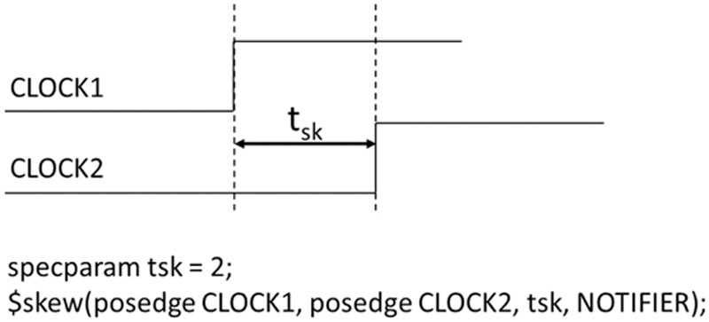
| $skew | Arrival times of two clock signals |
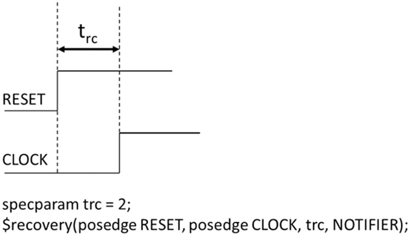
| $recovery | Time from reset release to clock arrival |
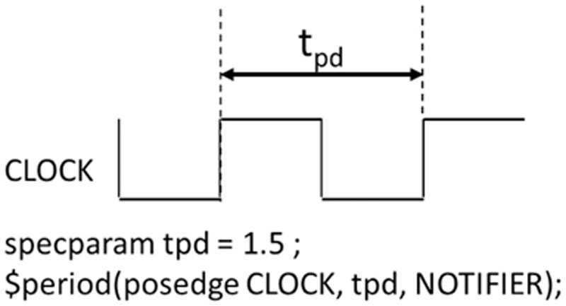
| $period | Clock period |
| $width | Clock duty cycle |
| $nochange | Stability between an edge and another signal |
Not all flipflop models will use all the timing checks. $recovery is only applicable to cells that have asynchronous reset or preset inputs. $setuphold covers both setup and hold timing checks in a single line, so using it with either of the first two would be redundant. $nochange can be used for the same purposes as setup and hold checks. Specifying both a minimum high- and low-width time makes a period check redundant.
$skew reports a violation if the time between edges is greater than the specified limit. The other checks shown in Table 11.2 all report a violation if the difference between the specified events is less than the limit.
$skew is used to check that there is not too much clock skew between active edges of two clock branches. It reports a violation if the active edge of the second clock does not occur within a given amount of time from the active edge of the first clock. This timing check is not normally found in cell models.
Timing checks are used with a special register called a “notifier.” Notifiers can be set to toggle when a timing check is violated. A notifier need not be initialized to any value to toggle. Verification code may be written to stop whenever a notifier changes state. Sequential UDPs will typically have an input for the notifier. When it toggles, the output is set to unknown. The D flipflop model of Figure 11.14 has been modified in Figure 11.15 to include a notifier. Notifier is not a keyword and may be used as the name of the notifier register. Any other legal Verilog identifier may be used as well.
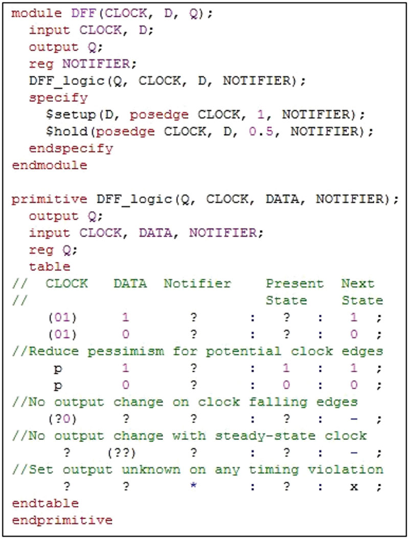
The model shown in Figure 11.15 has two timing checks. A violation of either will cause the notifier to toggle and the cell output to be set to unknown.
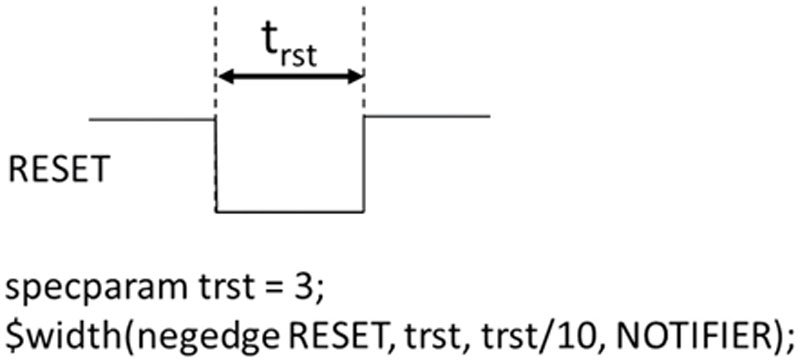
Common timing checks and examples of their usage are shown in Figures 11.16–11.20 . Checks may also have a second timing parameter specifying a threshold value to filter out spikes. The width timing check shown in Figure 11.20 is set so that a pulse shorter than the threshold value will not register as an error but one between the threshold and the width limit will. The threshold value in this case is the minimum width divided by 10.

Whether or not a timing check needs or can accept a threshold argument is implementation-dependent. There is considerable variation in the implementations of timing checks between design automation companies.
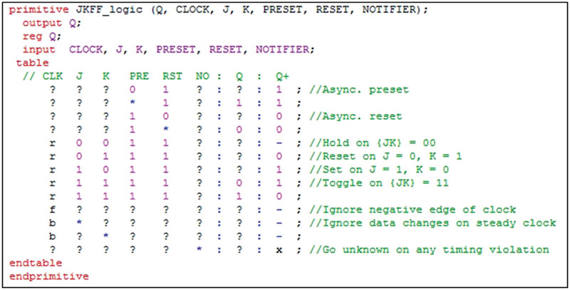
Flipflops that combine level and edge sensitivity add another level of complexity to models. Figure 11.21 shows a module for a model of a JK flipflop with active-low preset and reset inputs. The primitive for the model is shown in Figure 11.22.
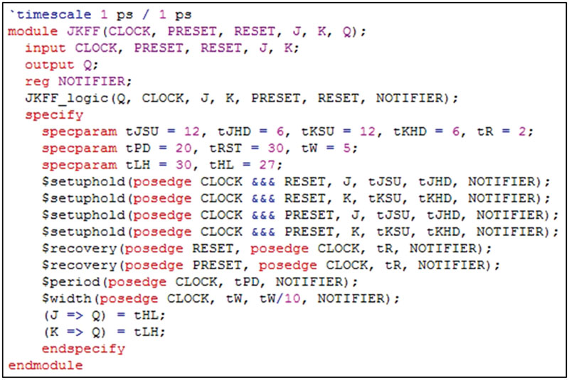
The specify block for the JK flipflop model includes conditions on setup and hold checks. They prevent setup and hold violations on the J and K inputs from causing a timing violation when either the preset or reset is active. The triple & is used to indicate a logical AND only in specify blocks. Timing checks can also use equality operators, case equality operators, negation, and XOR operators.
The UDP table has no entry for both preset and reset being simultaneously active. When that happens, the output will go unknown. This is deliberate, as the behavior of such a flipflop is unpredictable when the two inputs are both active.
Model performance
Chapter 2 emphasized the inefficiency of designing at the gate level. Up to this chapter, all subsequent coding had been done with behavioral constructs. Yet in modeling, primitive operators are back.
The reason for this is simulation performance. Models built from primitives, whether built-in or user-defined, simulate faster than behavioral code. The difference is significant. The D flipflop cell model of Figure 11.14 runs more than twice as fast as the behavioral model of a flipflop shown in Figure 11.23. Modifying the behavioral model of Figure 11.23 to set the output unknown for any timing violation would substantially complicate the model and further slow it down, increasing the advantage of using a table for such a cell.

Summary
Once a design is verified, it is turned into a technology-dependent netlist through logic synthesis. This netlist may only be simulated if there are cell models for the targeted semiconductor process.
Cell models are built from primitive operators. These operators can be the built-in ones introduced in Chapter 2 or they can be user-defined cells.
Besides defining the behavior of a cell, a model will also define its timing. For combinational cells, this is just the propagation paths from inputs to outputs. Sequential cells also need timing checks to detect operating violations such as setup and hold times. When a timing violation is detected in simulation, the cell output is set to unknown.
Designing with primitive operators remains a tedious and error-prone exercise. Behavioral code is far more efficient for design. Once a design has been verified and synthesized, it may be resimulated to ensure proper timing. This requires a library of cell models that do use primitive operators along with timing data. The primitives used in cell models may be the built-in Boolean primitives or user-defined functions. Combinational cells are almost always constructed with the built-in primitives. Sequential cells almost always use a table to define behavior. Because a table can only have one output, tables are often supplemented with one or more instances of built-in primitives to complete a model of a complex cell.