3
Component symbols
On a road map, symbols illustrate towns, cities, secondary roads, primary roads, airports, railroad tracks, and geographical landmarks. The same rule applies to schematic drawings; symbols indicate conductors, resistors, capacitors, solid-state components, and other electronic parts. Every time a new component comes out, a new schematic symbol is derived for it. Often, a new type of component is a modification of one that already exists, so the new schematic symbol ends up as a modification of the symbol for the preexisting component.
Tip
In this chapter, you’ll find most of the schematic component symbols commonly used in electricity and electronics. Appendix A contains a more complete listing in alphabetic, tabular form. You’ll find it in the back of this book.
Resistors
Resistors are among the most simple electronic components. As the term implies, they resist the flow of electrical current. The value or “size” of a resistor is measured in units called ohms; typical real-world resistors are rated from about one ohm up to millions of ohms. Less commonly, you’ll encounter resistors with values of less than an ohm, or hundreds of millions (or even billions) of ohms.
Regardless of the ohmic value, all fixed-value resistors are schematically indicated by the symbol shown in Fig. 3-1. This is the most universally accepted symbol for a resistor. The two horizontal lines indicate the leads or conductors that exit from both ends of the physical component. (Sometimes the resistor contacts are not wire leads but more substantial metal terminals.) Figure 3-2 shows a “transparent” functional drawing of a carbon-composition fixed resistor with leads on both ends. Figure 3-3 shows pictorial drawings of two other types of resistors. Any resistor of the sort shown pictorially in Fig. 3-2 or Fig. 3-3 is indicated schematically by the symbol in Fig. 3-1.

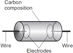
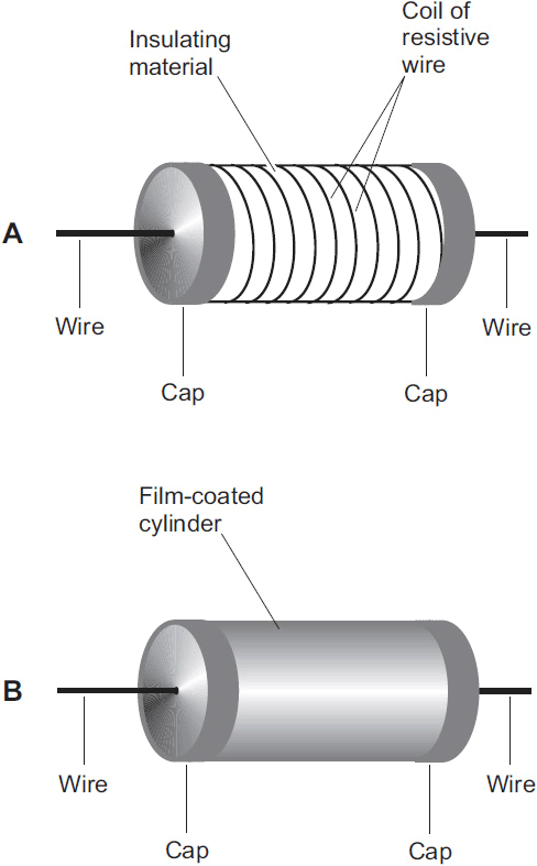
FIG. 3-3. Pictorial illustrations showing the anatomy of a wirewound resistor (at A) and a film type resistor (at B).
A variable resistor has the ability to change ohmic value by means of a slide or rotary tap that can be moved along the resistive element. The variable resistor is usually set to one value, and it remains at this point until manually changed. The electronic circuit, therefore, “sees” the component as a fixed resistor. However, when a variable resistor is required for the proper functioning of a specific circuit, it is necessary to indicate to any person who might build it from a schematic drawing that the resistor is actually a variable type. Figure 3-4 shows the schematic symbol for a variable resistor with two leads. Other types of variable resistors exist, and they have three leads (two end leads and a tap). Figure 3-5 shows two examples of schematic symbols for a three-terminal variable resistor, known as a potentiometer or a rheostat depending on the method of construction. Notice that both examples use the standard resistor configuration, and indicate that it’s a variable type by means of an arrow symbol pointing to the zig-zag part.
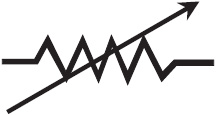
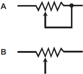
FIG. 3-5. Alternate symbols for variable resistors, also known as potentiometers or rheostats (depending on the physical construction method). The device at A connects one end to the tap; and the device at B uses a three-terminal arrangement.
Rheostats are in effect the same as potentiometers, but mechanically they differ. A rheostat contains a wirewound resistance element, while a potentiometer is normally of the carbon-composition type. Therefore, a rheostat’s value varies in small increments or steps, while a potentiometer’s value can be adjusted over a continuous range.
In schematic drawings, an arrow often indicates variable properties of a component, but not always! Transistors, diodes, and some other solid-state devices have arrows in their schematic symbols. These arrows don’t have anything to do with variable or adjustable properties. Arrows can also sometimes indicate the direction of current or signal flow in complex circuits.
Figure 3-6 is a pictorial drawing of a variable resistor of the wire-wound type, manufactured so that the resistance wire is exposed. A sliding metallic collar, which goes around the body of the resistor, can be adjusted to intercept different points along the coil of resistance wire. The collar is attached by a flexible conductor to one of the two end leads. The collar, therefore, shorts out more or less of the coil turns, depending on where it rests along the length of the coil. As the collar moves toward the opposite resistor lead, the ohmic value of the component decreases.
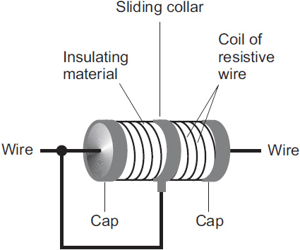
Figure 3-7 shows a functional drawing of a rotary potentiometer (at A), along with the schematic symbol (at B). The symbol looks like the variable resistor equivalent, but has three discrete contact points. Using the potentiometer control, the portion of the circuit that comes off the arrow lead can be varied in resistance to two circuit points, each connected to the two remaining control leads. Figure 3-8 shows a pictorial drawing of a typical potentiometer.
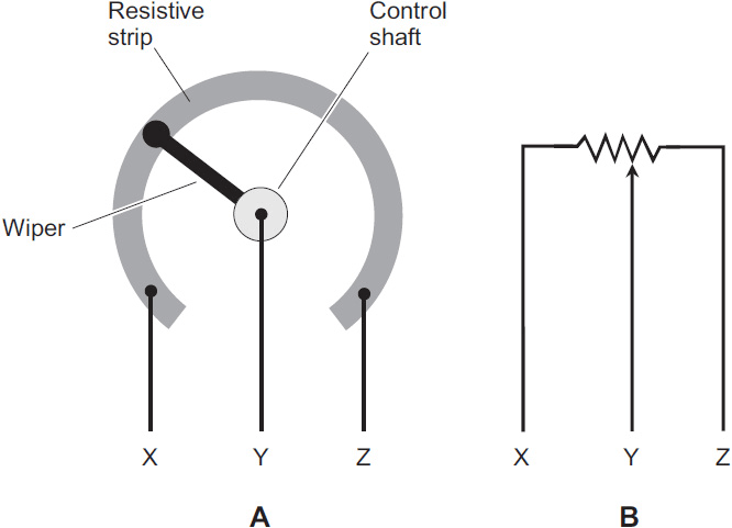
FIG. 3-7. Simplified functional drawing of a rotary potentiometer (A) and its schematic symbol with corresponding connections (B).
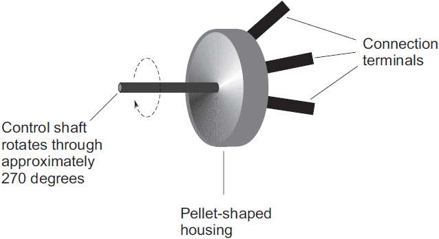
FIG. 3-8. Pictorial drawing of a full-size potentiometer, suitable for mounting on the front panel of an electronic device such as a radio receiver.
The variable resistor shown pictorially in Fig. 3-6 can be changed into a rheostat by severing the connection between the collar and the end. Now, the collar can be used as the third or variable contact. Likewise, a rheostat or potentiometer can be turned into a two-lead variable resistor by shorting out the variable contact point with the lead on either end.
The schematic symbol for a resistor, all by itself, tells us nothing about the ohmic value, or anything else about the component such as its power rating or physical construction, either. Various specifications for the component can be written alongside the resistor symbol, but these details might also appear in a separate components table and referenced by an alphabetic/numeric designation printed next to the schematic symbol (such as R1, R2, R3, and so on).
Tip
You can usually determine the ohmic value of a fixed resistor by looking at the colored bands or zones on it. Appendix B lists the resistor color codes that specify the ohmic values of fixed resistors.
Capacitors
Capacitors are electronic components that have the ability to block direct current (DC), while passing alternating current (AC). They also store electrical energy. The basic unit of capacitance is the farad (symbolized F). The farad is a huge electrical quantity, and most real-world components are, therefore, rated in tiny fractions of a farad—microfarads or picofarads. A microfarad (symbolized µF) equals a millionth of a farad (0.000001 F), and a picofarad (symbolized pF) equals a millionth of a microfarad (0.000001 µF) or a trillionth of a farad (0.000000000001 F).
Figure 3-9 shows the common schematic symbol for a fixed capacitor. On occasion, you might see alternative symbols, such as those in Fig. 3-10. Many different types of capacitors exist. Some are nonpolarized devices, meaning that you can connect them in either direction and it doesn’t make any difference. Others are polarized, having a positive and a negative terminal, and you must take care to connect them so that any DC voltage that happens to appear across them has the correct polarity. Most types of capacitors contain only two leads, although every now and then, you’ll come across one with three or more leads.

FIG. 3-9. Standard symbol for a fixed capacitor. The curved line represents the plate (or set of plates) electrically closer to ground.
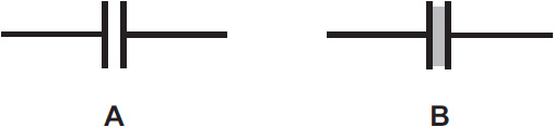
The basic capacitor symbol consists of a vertical line followed by a space and then a parenthesis-like symbol. Horizontal lines connect to the centers of the vertical line and the parenthesis to indicate the component leads. The parenthesis side of a capacitor indicates the lead that should go to electrical ground, or to the circuit point more nearly connected to electrical ground. Unless the symbol includes a polarity sign, it indicates a nonpolarized capacitor, which might be made from metal plates surrounding ceramic, mica, glass, paper, or other solid nonconducting material (and, in some cases, air or a vacuum). The material designation indicates the insulation, technically known as a dielectric, that separates the two major parts of the component. Physically, a typical fixed-value capacitor comprises two tiny sheets of conductive material close to each other but kept electrically separated by the dielectric layer.
Figure 3-11 shows the schematic symbol for a polarized or electrolytic capacitor. Notice that this symbol is the same as the one for the nonpolarized component, but a plus (+) sign has been added to one side. This sign indicates that the positive terminal of the component goes to the external circuitry. Occasionally, a negative (–) symbol will also appear on the opposite side. When you see the plus sign, you know that the component is polarized, and therefore, that you must connect it to the remainder of the circuit in observance of the proper polarity. That means the positive capacitor electrode must go to the more positive DC voltage point in the circuit, and the other electrode must go to the more negative DC voltage point in the circuit.
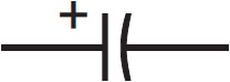
FIG. 3-11. Schematic symbol for a polarized capacitor. The side with the plus sign (+) should carry a positive voltage relative to the other side.
Tip
Polarized capacitors have external markings that tell you the polarity. Some have a plus sign, and some have a minus sign, and a few have both. Often, you’ll need a magnifying glass to resolve the symbols, so beware: You should never connect a polarized capacitor the wrong way around!
All the capacitors that we’ve seen so far have a fixed design. In other words, the components specified have no provision for changing the capacitance value, which is determined at the time of manufacture. Some capacitors, however, do have the ability to change value. These components are generally called variable capacitors, although some specialized types are known as trimmer capacitors or padder capacitors.
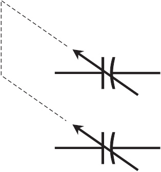
Figure 3-12 shows the most common symbol for a variable capacitor. An arrowed line reveals the variable property; it runs diagonally through a fixed capacitor symbol. Figure 3-13 shows two alternative ways of indicating this same component. Most of the time, the symbol shown in Fig. 3-12 will indicate a variable capacitance, regardless of the physical construction details.
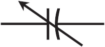
FIG. 3-12. Standard symbol for a variable capacitor. The curved line represents the rotor, and the straight line represents the stator.
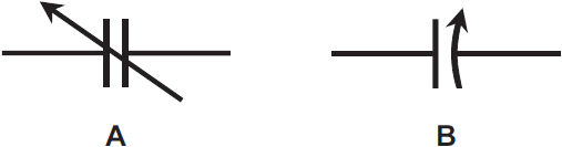
FIG. 3-13. Alternate symbols for variable capacitors. At A, the stator is not distinguished from the rotor; at B, the rotor appears as a curved line with an arrow.
An air variable capacitor (one with an air dielectric) can tune many types of radio-frequency (RF) equipment including antenna matching networks, transmitter output circuits, and old-fashioned radios. A typical air variable has many interlaced plates, with the plates connected together alternately to form two distinct contact points. The set of plates that you can rotate is called the rotor; the set of plates that remains stationary is called the stator. All variable capacitors are nonpolarized components, meaning that the external DC voltage you connect to them can go either way and it doesn’t make any difference.
Tip
In most air variables, the rotor should go to electrical ground. The rotor connects physically to the shaft that you turn. By grounding that shaft along with the rotor, you minimize external capacitance effects so that if you touch the shaft, the addition of your body into the system doesn’t upset the performance of the circuit. In addition, you’re protected against the risk of electric shock when the shaft that you touch goes directly to ground!
Sometimes, two separate variable capacitors are connected together or ganged in a circuit. In a ganged arrangement, two or more units are used to control two or more electronic circuits, but both components are varied simultaneously by tying the rotors of the two units together. Figure 3-14 shows the schematic symbol for two variable capacitors ganged together. The minimum and maximum capacitance values of the two components might be the same, but they don’t have to be the same. They will, however, always track together. In a ganged system, when one of the capacitors increases in value, the others all increase as well.
As is the case with most electronic components, the schematic symbol for the capacitor serves only to identify it and to show whether it is fixed or variable, and if fixed, whether or not it is polarized. The component value might be written alongside the schematic symbol, or the component might be given a letter and number designation (for example, C1, C2, C3, and so on) for reference to a components list or table that goes along with the diagram.
Inductors and transformers
A basic inductor comprises a length of wire that is coiled up in order to introduce inductance into a circuit. Inductance is the property that opposes change in existing current; it acts in practice only while current increases or decreases. Coils or inductors can range in physical size from microscopic to gigantic, depending upon the inductance value of the component, and on the amount of current that it can handle.
The basic unit of inductance is the henry (symbolized H), a large electrical quantity. Most practical inductors are rated in millihenrys (symbolized mH), where 1 mH = 0.001 H, or in microhenrys (µH), where 1 µH = 0.001 mH = 0.000001 H. Occasionally, you’ll see an inductor whose value is specified in nanohenrys (nH), where 1 nH = 0.001 µH = 0.000000001 H.
Figure 3-15 shows the basic schematic symbol for an air-core inductor. The two leads are designated by straight lines that merge into the coiled part. An air-core coil has nothing inside the windings that can affect the inductance. Some air-core coils are wound from stiff wire and support themselves mechanically, and their cores do, in fact, comprise nothing but air. In most cases, however, a nonconductive and noninductive form made out of plastic, mica, or ceramic material serves as a support for the coil turns, keeping them in place and enhancing the physical ruggedness of the component.

Did you know?
In some old radio receivers, you’ll find air-core inductors wound around small waxed cardboard cylinders resembling short lengths of drinking straw. Some hobbyists even use waxed wooden dowels to support “air-core” coils!
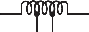
Figure 3-16 shows the schematic symbol for a tapped air-core inductor; in this case, the coil has two tap points along its length. Whereas the fixed coil had only two leads, a tapped coil has three or more. When a coil is tapped, separate conductors are attached to one or more of the turns for intermediate connection. Maximum inductance is obtained from connecting the end leads to the external circuitry. A tapped arrangement allows for the selection of an input or output point that offers lower inductance than the full coil does.
As an alternative to taps, a coil might have a sliding contact that can be advanced along the entire length of the windings. This sliding contact allows adjustment of the inductance value, rather than having a select fixed point with the tapping arrangement. A variable coil can be indicated by either of the symbols shown in Fig. 3-17. The arrow indicates that the component can be adjusted from a maximum inductance value to a minimum inductance value.
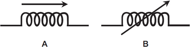
FIG. 3-17. Schematic symbols for a variable air-core inductor. At A, arrow above coil symbol; at B, arrow passing through coil symbol.
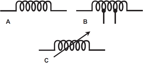
Figure 3-18 shows symbols for a fixed air-core coil (at A), a tapped air-core coil (at B), and an adjustable air-core coil (at C).
An inductor meant for low-frequency applications can consist of a coiled wire wound around a solid or laminated (layered) iron core. Here, the iron, which constitutes a ferromagnetic material, replaces the previous empty or air core. For example, a 60-Hz choke, intended for use in power-supply filters, will usually contain a single coil wound around a circular iron form. The ferromagnetic material greatly increases the magnetic flux density inside the coil windings, thereby increasing the inductance by a factor of many hundreds, or even thousands, of times compared with the inductance of an air-core coil having the same physical dimensions.
Figure 3-19 shows the schematic symbol for an iron-core inductor. Notice that it is the basic fixed coil discussed earlier, along with two close-spaced straight lines that run for its entire length. Sometimes the iron-core inductor is drawn as shown in Fig. 3-20, with the straight lines inside the coil turns in the symbol. (This is not the approved method of indicating an iron-core inductor, but you’ll still see it now and then.) Some iron-core inductors contain taps for sampling different inductance values, and some might even be adjustable. The equivalent schematic symbols for these types of components appear in Fig. 3-21.
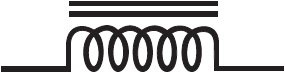

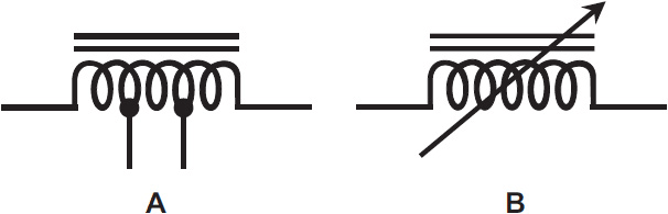
FIG. 3-21. Symbols for a tapped coil (A) and an adjustable coil (B) with solid- or laminated-iron cores.
At higher frequencies, solid-iron and laminated-iron cores aren’t efficient enough to function in inductors. Engineers would say that they have too much loss. At frequencies above a few kilohertz (kHz), a special core is needed if you want to increase the inductance over what you can get with nonferromagnetic core materials, such as air, plastic, ceramic, or wood. The most common substance for this purpose consists of iron material that has been shattered into myriad tiny fragments, each of which has a layer of insulation applied to it. After the fragmentation and insulation process has been completed, the particles are compressed to form a physically solid sample called a powdered-iron core. Figure 3-22 shows schematic symbols for powdered-iron-core inductors.
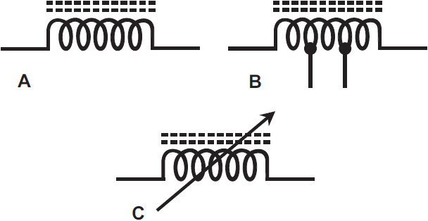
FIG. 3-22. Schematic symbols for fixed (A), tapped (B), and adjustable (C) inductors with powdered-iron cores.
The symbols for powdered-iron-core inductors are nearly identical to those for solid- or laminated-iron-core inductors, except that the straight lines are broken up instead of solid. These types of components, like all other types of inductors, can be tapped or continuously variable.
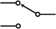
A transformer is made up of multiple inductors with the coil turns interspersed or wound around different parts of a single core. Figure 3-23 shows the symbol for a basic air-core transformer. It looks like two air-core coils drawn back-to-back. A transformer has the ability to transfer AC energy from one circuit to another at the same frequency. Because transformers are made by combining inductors, the schematic symbols are similar. Figure 3-24 shows some transformers that contain iron cores. The ones at A and B have solid or laminated cores; the ones at C and D have powdered cores.
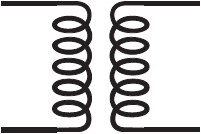
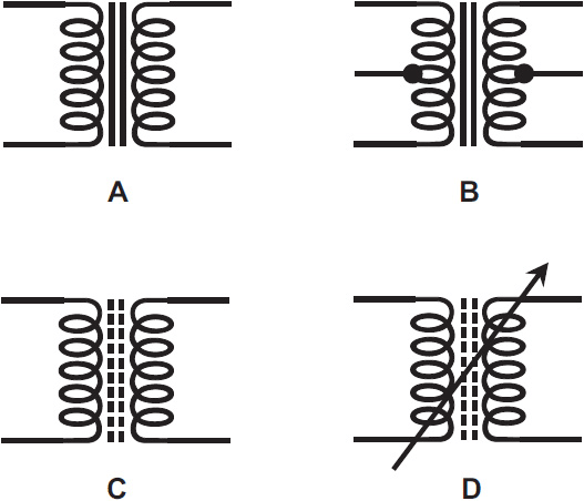
FIG. 3-24. At A, a transformer with a solid- or laminated-iron core. At B, a transformer with a solid- or laminated-iron core and tapped windings. At C, a transformer with a powdered-iron core. At D, an adjustable transformer with a powdered-iron core.
Switches
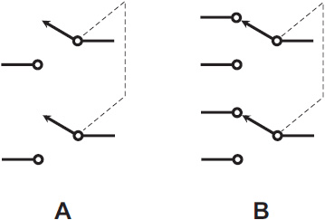
A switch is a device, mechanical or electrical, that completes or breaks the path of current. Additionally, a switch can be used to allow current to pass through different circuit elements. Figure 3-25 shows the schematic symbol for a single-pole/single-throw (SPST) switch. This component can make or break a contact at only one point in a circuit; it’s a two-position device (on-off or make-break).
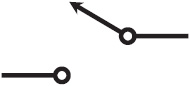
Figure 3-26 shows a different type of switch, designated as a single-pole/double-throw (SPDT) component. Symbolically, the pole coincides with the point of contact at the base of the arrowed line. A throw is the contact point to which the arrow can point. The SPDT switch contains one pole contact and two throw positions; the input to the pole can be switched to either the upper or lower circuit point.
Some switches contain two or more poles. Figure 3-27A shows the symbol for a double-pole/single-throw (DPST) switch, while Fig. 3-27B shows the symbol for a double-pole/double-throw (DPDT) switch. Some switches have even more elements. The one shown in Fig. 3-28 has five poles, each of which can be switched to two separate positions. Engineers and technicians might call it a five-pole/double-throw (5PDT) arrangement.
This last designation can actually be covered under the heading of multicontact switches. This category takes in most switches that have more than two poles or two throw positions. For example, a rotary switch has a single pole and several throw positions; Fig. 3-29 shows an example. The arrow still indicates the pole contact. In this case the switch has 10 throw positions. Technically, then, it’s a single-pole/10-throw (SP10T) device!
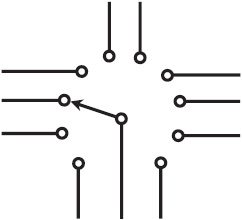
FIG. 3-29. Schematic symbol for a rotary (or wafer) switch. This one has a single pole and 10 throws (SP10T).
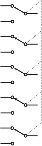
Occasionally, you’ll encounter sets of rotary switches ganged together, much like two or more variable capacitors can be made to rotate in sync with one another. Figure 3-30 shows the schematic symbol for an arrangement that uses two rotary switches. The dashed line tells us that the two switches are ganged. The two arrowed lines, which indicate the throw positions, go around “in sync” with each other. So, for example, when the left-hand switch (or pole number 1) rests at throw number 3 (as is the case here), the right-hand switch (or pole number 2) also rests at throw number 3.
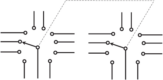
FIG. 3-30. Schematic symbol for two rotary switches ganged together. This one has two poles and 10 throws (2P10T).
In each case, every switch contact point (pole or throw) is represented by a tiny circle. The variable element or pole is indicated by an arrow. The symbols shown here are all standard. You’ll seldom see any significant variations.
Did you know?
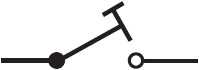
Some amateur radio operators use a special switch called a Morse code key. This old-fashioned device, also called a hand key or a straight key, makes or breaks a circuit for the purpose of sending Morse code manually. It’s an SPST switch with a lever and a spring, causing the device to return to the off position when the operator lets go of the lever. Figure 3-31 shows its schematic symbol.
Conductors and cables
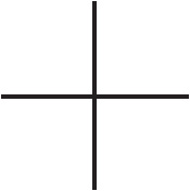
Throughout this discussion, a straight line has always indicated a conductor, but most circuits contain a large number of conductors. When you draw a diagram of a complicated circuit or system, you’ll often find it necessary to have lines cross over each other, whether the represented wires actually make contact in the physical system or not.
Figure 3-32 shows two conductors that must cross each other in a diagram, but that are not connected to each other in the physical circuit (at least not at the point where they cross in the schematic). This diagram geometry does not imply that when you build the circuit, the conductors must physically cross over each other at that exact place. It simply means that in order to make the schematic drawing, you have to draw one conductor across another to reach various circuit points without introducing a whole lot of confusion and clutter, or resorting to three dimensions to make your drawing.
Aha!
A real-world circuit exists in three-dimensional (3D) space, but when you want to diagram it, you must do it on a two-dimensional (2D) surface. To carry off that feat, you must learn a few tricks to make sure that your readers see things right!
Figure 3-33 shows two ways of portraying a point where two wires cross and they are electrically connected at that point. In the drawing at A, one of the conductors is “broken in two” so that it appears to contact the other one at two different points. This geometry makes it clear that the two conductors (the “divided” vertical one and the “solid” horizontal one) connect to each other electrically. Black dots indicate electrical connection. In the drawing at B, the two conductors cross (at right angles in this example), and a single black dot is drawn at the junction. This dot tells us that the conductors connect at this point. The method shown at B might look better at first glance, but the neatness comes along with a problem: Some readers might overlook the black dot and think that the two conductors are not meant to connect. The method at A makes that potential misinterpretation impossible.
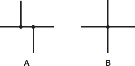
FIG. 3-33. At A, preferred symbol for conductors that intersect and are electrically connected to each other. At B, alternate symbol for the same situation.
Just as a reader might miss a black dot at a crossing point, as in Fig. 3-33B, another reader might see Fig. 3-32 and imagine a black dot when it isn’t there! Then the reader will think the two wires connect when in fact they do not. This problem rarely occurs in well-engineered schematics where the draftsperson makes sure to use big black dots and good quality printing presses. However, in some older schematics you will see nonconnecting, crossed wires shown as in Fig. 3-34. One of the wires has a half loop that makes it look like it jumps over the other wire to avoid contact. That trick (which should never have gone out of style, in my opinion) gets rid of any doubt as to whether the wires electrically connect at the crossover point or not.
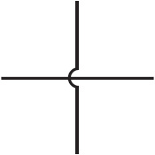
FIG. 3-34. Archaic (but clear) representation of conductors that cross paths but are not electrically connected to each other.
A cable consists of two or more conductors inside a single insulating jacket. In many cases, unshielded cables are not specifically indicated in a schematic drawing, but appear as two or more lines that run parallel to indicate multiple conductors. Shielded cables require additional symbology along with the conductors. Figure 3-35 shows examples of shielded wire, often used to indicate the use of coaxial cable in an electronic circuit. Coaxial cable contains a single wire called the center conductor surrounded by a cylindrical, conduit-like conductive shield. An insulating layer, called the dielectric, keeps the two conductive elements isolated from each other. In most coaxial cables, the dielectric material consists of solid or foamed polyethylene.
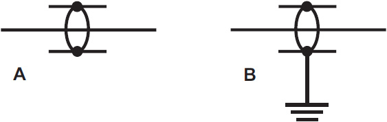
FIG. 3-35. At A, symbol for a coaxial cable with an ungrounded shield. At B, symbol for a coaxial cable with an earth-grounded shield.
Figure 3-36 shows a symbol for coaxial cable when the shield connects to a chassis ground, such as the metal plate on which an electronic circuit is constructed. The chassis ground might lead to an earth ground, but that’s not always the case. In a truck, for example, no earth ground exists, so the chassis of the trucker’s CB radio would go to the vehicle frame.
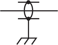
In some cables, a single shield surrounds two or more conductors. Figure 3-37 shows the schematic symbol for a two-conductor shielded cable. This symbol is identical to the one for coaxial cable, except that an extra inner conductor exists. If more than two inner conductors exist, then the number of straight, parallel lines going through the elliptical part of the symbol should equal the number of conductors. For example, if the cable in Fig. 3-37 contained five conductors, then five horizontal lines would run through the elliptical part of the symbol.
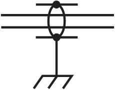
FIG. 3-37. Symbol for a shielded two-conductor cable, in this case with a chassis ground for the shield.
Diodes and transistors
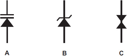
Figure 3-38 shows the basic symbol for a semiconductor diode. In this symbol, an arrow and a vertical line indicate parts of the diode, and the horizontal lines to the left and right indicate the leads. The symbol in Fig. 3-38 portrays a rectifier diode. The arrowed part of the symbol corresponds to the diode’s anode, and the short, straight line at the arrow’s tip corresponds to the cathode. Under normal operating conditions, a rectifier diode conducts when the electrons move against the arrow, i.e., when the anode has a positive voltage with respect to the cathode.
Figure 3-39 shows the symbols for some specialized diode types. At A, we see a varactor diode, which can act as a variable capacitor when we apply an adjustable DC voltage to it. At B, we see a Zener diode, which can serve as a voltage regulator in a power supply. At C, we see a Gunn diode, which can act as an oscillator or amplifier at microwave radio frequencies.
A silicon-controlled rectifier (SCR) is, in effect, a semiconductor diode with an extra element and corresponding terminal. Its schematic symbol appears in Fig. 3-40. In the SCR representation, a circle often (but not always) surrounds the diode symbol, and the control element, called the gate, shows up as a diagonal line that runs outward from the tip of the arrow. In all cases, the lead that goes to the base of the arrow is the anode of the device, and the one connected to the short straight line at the arrow’s tip is the cathode.
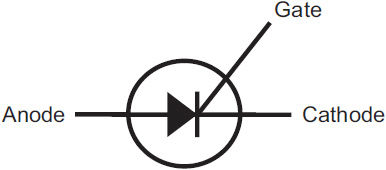
Figure 3-41 shows the schematic symbols for bipolar transistors. The PNP type is shown at A, followed by the NPN variety at B. The only distinction between the two is the direction of the arrow. In the PNP device, the arrow points into the straight line for the base electrode. In the NPN device, the arrow points outward from the base. Occasionally, the circle that surrounds the base, emitter, and collector leads is omitted from the bipolar transistor symbol. Besides the bipolar variety, many other types of transistors exist. Figure 3-42 shows the symbols for four of these devices, as follows:
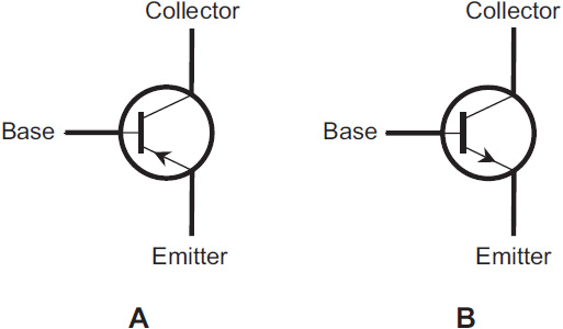
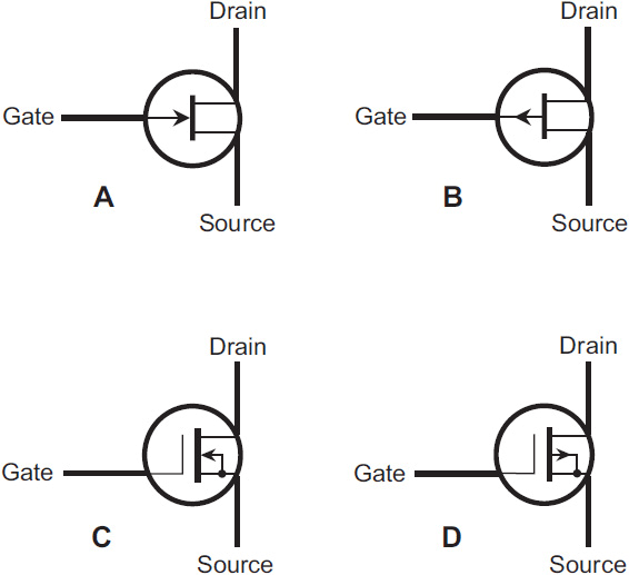
FIG. 3-42. At A, symbol for an N-channel JFET. At B, symbol for a P-channel JFET. At C, symbol for an N-channel MOSFET. At D, symbol for a P-channel MOSFET.
• At A, we see an N-channel junction field-effect transistor (JFET).
• At B, we see a P-channel JFET.
• At C, we see an N-channel metal-oxide-semiconductor field-effect transistor (MOSFET).
• At D, we see a P-channel MOSFET.
Tip
Transistors can be made from various types of semiconductor materials and metal-oxide compounds, but the schematic symbol, all by itself, tells us nothing about the elemental semiconductor material used in manufacture. The symbol merely indicates component functionality.
Electron tubes
Although vacuum tubes aren’t used in electronics nearly as often as they were a few decades ago, many designs still exist that do employ them. When you want to create the symbol for a vacuum tube, you should start by drawing a fairly large circle, and then you should add the necessary symbols inside the circle to symbolize the type of tube involved. Figure 3-43 shows the schematic symbols for the various types of tube elements commonly used in schematic drawings.
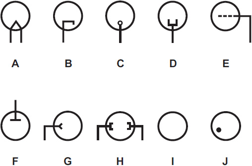
FIG. 3-43. Symbols for tube elements and characteristics. A: Filament or directly heated cathode. B: Indirectly heated cathode. C: Cold cathode. D: Photocathode. E: Grid. F: Anode (plate). G: Deflection plate. H: Beam-forming plates. I: Envelope for vacuum tube. J: Envelope for gas-filled tube.
Figure 3-44 shows the schematic symbol for a diode vacuum tube. This two-element device contains an anode (also called a plate) and a cathode. Just as with the semiconductor diode, the anode is normally positive with respect to the cathode when the device conducts current. The cathode emits electrons that travel through the vacuum to the anode. A hot-wire filament, something like a miniature lowwattage light bulb, heats the cathode to help drive electrons from it. In Fig. 3-44, the filament has been omitted for simplicity, a common practice in all vacuum tube symbology when the filament and cathode are physically separate, an arrangement known as an indirectly heated cathode.
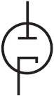
FIG. 3-44. Schematic symbol for a diode vacuum tube with an indirectly heated cathode. Although a filament exists, it is often omitted to reduce clutter in symbols for tubes with indirectly heated cathodes.
All tube elements are surrounded by a circle, which represents the tube envelope. Occasionally, the circle is omitted from some tube symbols in schematic drawings, but that’s not standard practice.
Figure 3-45 shows two versions of a triode vacuum tube, which consists of the same elements as the diode previously discussed, with the addition of a dashed line to indicate the grid. But there’s another difference, too, in drawing A. Can you see it? Look closely at the cathode. The tube at A has a directly heated cathode, in which the filament and the cathode are the very same physical object! We apply the negative cathode voltage directly to the filament wire; no separate cathode exists at all. In Fig. 3-45B, we see the symbol for a triode tube with an indirectly heated cathode. In this symbol, the filament is inside the cathode, which comprises a metal cylinder running along the central vertical axis of the tube.
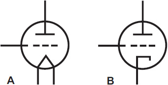
FIG. 3-45. Symbols for a triode tube with a directly heated cathode (A) and an indirectly heated cathode (B).
Tetrode vacuum tubes have two grids. To represent one of them, we need an additional dashed line, as shown in the drawings of Fig. 3-46. In the tetrode, the upper grid, closer to the anode, is called the screen. Figure 3-47 shows symbols for the so-called pentode tube, which has three grids and a total of five elements. In the pentode, the second grid (going from the bottom up) is the screen, and the third grid (just underneath the plate) is called the suppressor. In both Figs. 3-46 and 3-47, the left-hand symbol (at A) portrays a device with a directly heated cathode, while the right-hand drawing (at B) shows a device with an indirectly heated cathode.
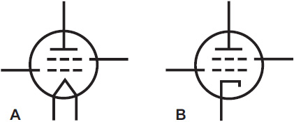
FIG. 3-46. Symbols for a tetrode tube with a directly heated cathode (A) and an indirectly heated cathode (B).
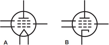
FIG. 3-47. Symbols for a pentode tube with a directly heated cathode (A) and an indirectly heated cathode (B).
In all the vacuum tube symbols shown here, electrons normally flow from the bottom up. They come off the cathode, travel through the grid or grids (if any), and end up at the plate. Once in awhile you’ll see a vacuum tube symbol lying on its side. In that sort of situation, you can simply remember that the electrons go from the cathode to the plate under normal operating conditions.
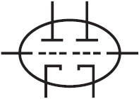
Some vacuum tubes consist of two separate, independent sets of electrodes housed in a single envelope. These components are called dual tubes. If the two sets of electrodes are identical, the entire component is called a dual diode, dual triode, dual tetrode, or dual pentode. Figure 3-48 shows the schematic symbol for a dual triode vacuum tube with indirectly heated cathodes.
In some older radio and television receivers, tubes with four or five grids were sometimes used. These tubes had six and seven elements, respectively, and were called hexodes and heptodes. These esoteric devices were used mainly for mixing, a process in which two RF signals having different frequencies are combined to get new signals at the sum and difference frequencies. The schematic symbol for a hexode is shown in Fig. 3-49A; the symbol for a heptode is shown in Fig. 3-49B. Some engineers called the heptode tube a pentagrid converter. Both of these symbols show devices with indirectly heated cathodes.
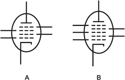
FIG. 3-49. At A, symbol for a hexode tube. At B, symbol for a heptode tube, also known as a pentagrid converter.
You won’t encounter hexodes and heptodes in modern electronics, but if you like to work with antique radios, you should get familiar with them. But take this warning: You’ll probably have a difficult time finding a replacement component, should one of these relics go “soft” on you!
Cells and batteries
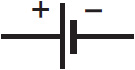
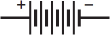
A cell or battery is often used as a power source for electronic circuits. Figure 3-50 shows the schematic symbol for a single electrochemical cell, such as the sort that you’ll find in a flashlight. A single-cell component such as this usually has an output of approximately 1.5 V DC. Electrochemical batteries with higher voltage outputs comprise multiple cells connected in series (negative-to-positive in a chain or string); the schematic representation for a multicell battery takes this design into account, as shown in Fig. 3-51.
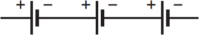
The multicell battery symbol is simply a number of single-cell symbols placed end-to-end without any intervening lines. If a circuit calls for the use of three individual, discrete single-cell batteries in a series connection, you might draw three cell symbols in series with wire conductor symbols between them (Fig. 3-52). Alternatively, if multiple individual cells are set in a “battery holder” designed for direct series connection, you can use a battery symbol to portray the whole bunch.
Standard practice calls for polarity signs to go with the symbols for cells or batteries. Unfortunately, some draftspeople neglect this detail. Then when you see the schematic, you’ll have to infer the polarity by scrutinizing the rest of the circuit.
Logic gates
All digital electronic devices employ switches that perform specific logical operations. These switches, called logic gates, can have anywhere from one to several inputs and (usually) a single output. Logic devices have two states, represented by the digits 0 and 1. The 0 digit is normally called “low” and the 1 digit is called “high.”
• A logical inverter, also called a NOT gate, has one input and one output. It reverses, or inverts, the state of the input. If the input equals 1, then the output equals 0. If the input equals 0, then the output equals 1.
• An OR gate can have two or more inputs (although it usually has only two). If both, or all, of the inputs equal 0, then the output equals 0. If any of the inputs equals 1, then the output equals 1. Mathematical logicians would tell us that such a gate performs an inclusive-OR operation because it “includes” the case where both variables are high.
• An AND gate can have two or more inputs (although it usually has only two). If both, or all, of the inputs equal 1, then the output equals 1. If any of the inputs equals 0, then the output equals 0.
• An OR gate can be followed by a NOT gate. This combination gives us a NOT-OR gate, more often called a NOR gate. If both, or all, of the inputs equal 0, then the output equals 1. If any of the inputs equals 1, then the output equals 0.
• An AND gate can be followed by a NOT gate. This combination gives us a NOT-AND gate, more often called a NAND gate. If both, or all, of the inputs equal 1, then the output equals 0. If any of the inputs equals 0, then the output equals 1.
• An exclusive OR gate, also called an XOR gate, has two inputs and one output. If the two inputs have the same state (either both 1 or both 0), then the output equals 0. If the two inputs have different states, then the output equals 1. Mathematicians use the term exclusive-OR operation because it doesn’t “include” the case where both variables are high.
Figure 3-53 illustrates the schematic symbols that engineers and technicians use to represent these gates in circuit diagrams.
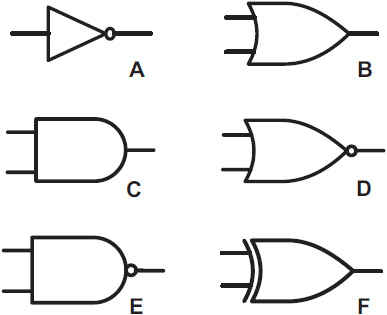
FIG. 3-53. Symbols for a logical inverter or NOT gate (A), an OR gate (B), an AND gate (C), a NOR gate (D), a NAND gate (E), and an XOR gate (F).
Summary
You’ll encounter lots of symbols in electronics other than the common ones shown in this chapter. Appendix A is a comprehensive table of schematic symbols. In addition to the ones already discussed, you will see symbols for jacks and plugs, piezoelectric crystals, lamps, microphones, meters, antennas, and many other electronic components.
It might, at first thought, seem like a massive chore to memorize all of these symbols, but their usage and correct identification will come to you with practice and with time. The best way to begin the learning process is to read simple schematics and refer to Appendix A in this book whenever a symbol crops up that you can’t identify. Within a few hours you’ll be able to move on to more complex schematics, again looking up the unknown symbols. After a few weekends of practice, you should be thoroughly familiar with most electronic symbols used in schematic representations, so that when you see one in a diagram, you’ll recognize it without having to think about it.
Schematic symbols are the fundamental elements of a communication scheme, like the symbols in mathematical expressions or architectural blueprints. Most schematic symbols in electronics are based on the structure of the components or devices they represent. Schematic symbols often appear in groups, each of which bears some relationship to the others. For example, you’ll encounter many different types of transistors, but they’re all represented in a similar fashion. Minor symbol changes portray variations in internal structure, but all can be easily identified as some type of transistor. The same rule applies to the symbols for diodes, resistors, capacitors, inductors, transformers, meters, lamps, and most other electronic components.