
Dynamic Range
Distortion and Noise
Publisher Summary
In engineering terms, dynamic range is the ratio between the largest and the smallest signals, and it is primarily wide dynamic range (not bandwidth) that distinguishes quality audio from rubbish. Provided that the largest signal is not clipped, maximizing dynamic range becomes a problem of minimizing the three unwanted signals that otherwise mask the smallest wanted signal: Distortion; Random noise; and Artificial interference, frequently referred to as Electromagnetic Compatibility (EMC). EMC is largely a construction issue and will be considered in Building Valve Amplifiers, so this chapter investigates how to minimize distortion and noise. To investigate and minimize distortion, one must begin by looking at the fundamentals of distortion measurement. Even designers of test equipment would probably concede that this is not the sexiest of topics, but unless one understands how errors can creep into our measurements, he/she will not have the confidence to compare the results of one measurement with those of the other, leaving one unable to test and improve the designs.
In engineering terms, dynamic range is the ratio between the largest and the smallest signals, and it is primarily wide dynamic range (not bandwidth) that distinguishes quality audio from rubbish. Provided that the largest signal is not clipped, maximising dynamic range becomes a problem of minimising the three unwanted signals that otherwise mask the smallest wanted signal:
EMC is largely a construction issue and will be considered in Building Valve Amplifiers, so this chapter will investigate how to minimise distortion and noise.
Distortion
To investigate and minimise distortion, we must begin by looking at the fundamentals of distortion measurement. Even designers of test equipment would probably concede that this is not the sexiest of topics, but unless we understand how errors can creep into our measurements, we will not have the confidence to compare the results of one measurement with those of the other, leaving us unable to test and improve our designs.
Defining Distortion
Although we may glibly use the word ‘distortion’ while talking about amplifiers, there are actually two distinct types of distortion.
Linear distortions do not change with amplitude. If we consider the transfer characteristic of a device producing linear distortion, it is a straight line – hence the term linear distortion (see Figure 3.1a).
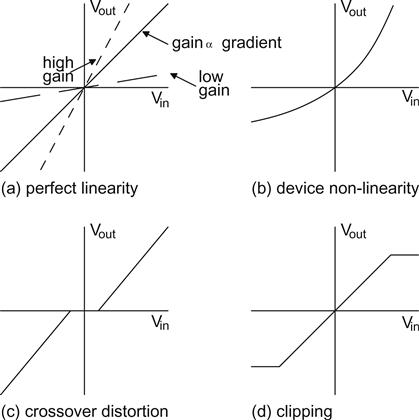
Although a device causing linear distortion changes the shape of the waveform, there are no additional frequencies at the output of the device. Linear distortion typically causes errors in the amplitude against frequency response – and this is the way that it is usually assessed. However, it is perfectly possible to change the shape of a waveform without changing the amplitude against frequency response by distorting the time at which frequencies arrive – loudspeaker crossover systems without delay compensation inevitably generate this distortion. The shape of a square wave’s leading edge is particularly sensitive to timing errors, so an oscilloscope quickly reveals problems. Alternatively, timing errors between sine waves of differing frequencies can be determined by measuring the gradient of a plot of phase against frequency (linear scale for frequency). Deviations from the expected straight line imply phase errors – hence the term linear phase for an ideal device.
Unsurprisingly, the transfer characteristic for non-linear distortion is not a straight line, and a device causing non-linear distortion has frequencies at the output that were not present at the input (see Figure 3.1b–d).
Measuring Non-Linear Distortion
We can assess the linearity of a device in two fundamental ways:
• We plot the transfer characteristic directly. Since the definition of non-linear distortion was that the transfer characteristic should deviate from a straight line, we could measure the deviations. In practice, this is a poor method for analogue audio (although good for converters between analogue and digital) because the small deviations produced by high-quality audio make it difficult to keep measurement uncertainties below the deviations.
• We look for frequencies at the output of the device that were not present at the input. This is a very sensitive and easily applied test, so there are two common variations on the theme.
The simplest expression of the second test is to apply a single sine wave to the device. At the output of the device, we expect to see a single sine wave. However, if the device produces non-linear distortion, there will also be harmonics of the original sine wave. The test is popular because removing the original sine wave at the output is easy, leaving only the harmonics – which can then be measured, either individually or collectively, as Total Harmonic Distortion (THD).
A more complex method is to apply two sine waves to the device. Again, we should only see these two frequencies at the output, but a device producing non-linear distortion causes the two frequencies to amplitude modulate one another, producing sum and difference frequencies known as intermodulation products. Intermodulation distortion measurement is popular with Radio Frequency (RF) engineers because it is easy to tune to each intermodulation product and measure its amplitude, but this is not quite so easily done at audio frequencies.
It is most important to realise that measuring harmonic distortion is no more ‘correct’ than measuring intermodulation distortion, or vice versa. Both forms of measurement simply reflect the same non-linearity in the device’s transfer characteristic. What is important is how the measurement is made and how the results are interpreted.
Distortion Measurement and Interpretation
In an ideal world, everybody would make their distortion measurement in the same way, with the same equipment, and interpret their results identically. All results would then be comparable, allowing us to state that device ‘A’ was better than device ‘B’.
In practice, there are many different measurement techniques. For example, the intermodulation distortion measurement requires two (or more) frequencies. Which frequencies should be chosen, and what should their relative amplitudes be? There are at least three standards for this measurement. Similarly, which frequency should we use for measuring harmonic distortion? Should we make the measurement at a single frequency, or should we sweep frequency through the entire audible range? Which results should we include, and which ones should we exclude? Standards attempt to answer these questions and allow results to be compared. Engineers love standards – that’s why we have so many of them.
If we have designed a piece of equipment, we already know where its failings are likely to be, so we plan our test to expose those failings. This allows us to quantify the failings, make a change to the design and measure to see if we have made an improvement.
The previous paragraph strikes to the heart of the measurement problem, and raises various points:
• We need to be aware of the limitations of the test equipment. There is little point in attempting to measure the distortion of an amplifier suspected to produce <0.01% Total Harmonic Distortion+Noise (THD+N) if the test oscillator itself produces 0.01% THD+N.
• We must know the relevance of our measurements. Measuring wow and flutter on an analogue turntable is useful because this measurement exposes known mechanical failings. Conversely, early CD player specifications quoted pointless wow and flutter measurements (essentially zero for a digital source), but failed to measure jitter (an insidious problem in the conversion between analogue and digital domains).
• A designer, seeking to improve their design, makes the test critical. Conversely, the marketing department requests engineering tests that the device is known to pass comfortably – such as harmonic distortion at 10 dB below full output for a digital source – because these tests give such good figures.
• Hopefully, nobody understands a given design as well as the designer – who is best placed to decide which tests should be made.
For these reasons, measurements quoted by manufacturers or reviewers are not necessarily particularly useful – and this is part of the reason for subjective reviews. (Another reason is that good test equipment is expensive.)
However, if we intend to design and build valve amplifiers, then carefully chosen measurements employing cheap test gear and careful interpretation can be very useful indeed.
Choosing the Measurement
Transistor amplifiers typically have plenty of global negative feedback to reduce distortion. Because applying feedback can easily turn an amplifier into an oscillator, the amplifier is deliberately made to have an amplitude response that falls with frequency before the feedback is applied. Since negative feedback reduces both linear and non-linear distortions, when it is applied the frequency response reverts to flatness and non-linear distortion is also reduced. However, because the amplifier’s response was falling with frequency before the feedback was applied, less negative feedback is available at high frequencies to correct non-linear distortion. This means that high-feedback amplifiers must have THD that rises with frequency, so a single-frequency measurement is inappropriate, and a swept measurement is better.
If we test a circuit that does not have global negative feedback, then a single-frequency measurement may be appropriate – if we know what causes the distortion.
A valve distorts because of the curvature in its Ia versus Vgk transfer characteristic, and does so at all audio frequencies without fear or favour. Harmonic distortion is the easiest measurement, and we are at liberty to choose any test frequency that we feel is convenient. We might choose 50 Hz or 60 Hz because we have a DVM specified to be accurate to 0.1 dB at that frequency. If we do, we will find that we cannot even measure the fundamental amplitude accurately because stray hum picked up from nearby power wiring beats with our wanted signal to give a gently fluctuating measurement. We need to change our test frequency so that it is clear of mains hum and its harmonics.
Perhaps we could use 10 kHz. This is nicely clear of mains hum, but has problems of its own. Some non-linearities produce mainly higher harmonics, but if the amplifier’s amplitude against frequency response was already falling, this would attenuate the very harmonics we were trying to measure, and give a falsely good result. We need a lower frequency.
In terms of octaves, 1 kHz is in the middle of the audio band, so it is least affected by errors caused by reduced bandwidth and is sufficiently far away from AC mains frequency for hum not to upset the result. Marketing people love 1 kHz because it measures so very well.
Refining Harmonic Distortion Measurement
Classical harmonic distortion measurements were made at 1 kHz by removing the 1 kHz fundamental and measuring the amplitude of the remaining signal. Although they were appropriate for the valve amplifiers of the time, these tests were rightly criticised when applied to transistor amplifiers because they took no account of the distribution of harmonics and their subjective annoyance.
Weighting of Harmonics
Various proposals have been made for weighting the levels of individual harmonics to allow harmonic powers to be summed to give a single-figure measure of subjective distortion.
Shorter [1] suggested in 1950 that levels should be weighted by a factor of n2/4 (where n is the number of the harmonic):
From n to 2n is one octave, so the gradient in dB/octave is:
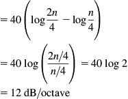
Thus, rather than measuring amplitudes of individual harmonics and calculating THD, a rising response of 12 dB/octave could be applied to a conventional distortion meter. In order that the measurement should be comparable with a conventional meter measuring pure second harmonic distortion from a 1 kHz source, the weighting filter would need a −12 dB gain offset to ensure 0 dB gain at 2 kHz. Note that the combination of the weighting filter and its gain offset means that weighted distortion measurements are only valid for the single specified fundamental frequency.
However, there are problems with the n2/4 weighting technique. Using the 1 kHz measurement example, 20 kHz is 10 times higher than 2 kHz, so the filter would add a minimum of 40 dB of gain to harmonics that are inaudible. Since the whole point of the exercise was that the measured result should agree with the subjective nuisance, a 20 kHz low-pass filter is also required.
Although the Shorter recommendation successfully ranked measured distortion against the subjective nuisance, the test suffered from the limitations of its time. The levels of deliberate distortion were quite high (0.41–3.7% RMS unweighted), and the loudspeaker was a ‘wide-range coaxial horn’ of unspecified distortion.
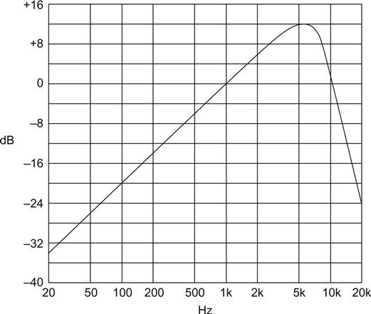
Peter Skirrow of Lindos Electronics argued that distortion should be measured at 1 kHz using a weighting filter conforming to CCIR468-2 because the response of this filter was determined by the subjective nuisance of different frequencies. Broadly speaking, CCIR468-2 rises with frequency at 6 dB/octave, has 0 dB gain at 1 kHz and peaks by 12 dB at 6.3 kHz, after which it falls swiftly (see Figure 3.2).
Summation and Rectifiers
The waveform that remains after the fundamental has been removed is known as the distortion residual and is composed of a number of harmonically related frequencies. How should we measure the amplitude of this waveform? This is not nearly as easy a question as it first appears. Perhaps we could measure Vpk–pk (see Figure 3.3).
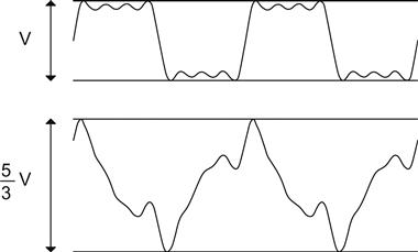
Both waveforms are square waves with correct amplitude harmonics up to the seventh harmonic, and none thereafter, but one has had the phase of the fundamental shifted by 90°, which significantly changes Vpk–pk. Mathematically, the correct way to sum individual harmonics is to turn the voltages into powers by squaring (P=V2/R), take the mean of the powers, and then convert this back into a voltage by taking the square root, otherwise known as an RMS measurement. Thus, classical distortion measurements measure the amplitude of the distortion residual using a meter incorporating a true RMS rectifier, and their measurements may reflect this fact by quoting THD in %RMS.
Alternative Rectifiers
CCIR468-2 specifies that the rectifier should be peak detecting, because noise is impulsive, and we want to capture the amplitude of these noise spikes. Crossover distortion produces narrow spikes that would contribute very little to an RMS summation, but are subjectively extremely annoying, so the peak-detecting rectifier of CCIR468-2 would seem ideal for detecting these spikes.
CCIR468-2 is not quite ideal because it needs the previously mentioned gain offset, so the CCIR/ARM recommendation offsets the gain of the CCIR468-2 weighting filter by 6 dB to give 0 dB gain at 2 kHz, allowing it to be used for 1 kHz distortion weighting. Unfortunately, it also changes the rectifier from peak detecting to average reading (ARM, Average Reading Meter), marking it less likely to detect the spikes produced by crossover distortion, so you might prefer to use CCIR468-2 and add the gain offset manually.
Noise and THD+N
Although using a CCIR468-2 filter to weight distortion is cheap and effective, its rising response with frequency may create another problem. Properly designed circuitry creates very little distortion. To put it another way, the distortion could be of comparable amplitude to the noise that all electronics generates. When we make our THD measurement, using our meter, how do we know that we are not actually measuring the amplitude of the noise?
The best solution is to view the distortion residual on a 20 MHz oscilloscope (or one with the 20 MHz filter engaged). If the waveform appears clean, we are measuring mostly distortion; if a repetitive waveform is difficult to discern, we are probably measuring noise. Thus, all practical measurements made by a meter are actually THD+N, and we have to be certain that the noise is sufficiently small to be ignored. Digital oscilloscopes are excellent for making this decision objectively. The oscilloscope can be set to measure the RMS amplitude of the distortion residual, and this measurement can be compared with the same measurement but with averaging engaged. Averaging multiple waveforms cancels the noise (which is random), but maintains the repetitive distortion residual. If there is negligible (<10%) difference between the two measurements, we are measuring distortion. But if the averaged value drops to 71% of the unaveraged value, we are measuring equal amounts of noise and distortion residual, and it is time to stop recording distortion figures.
By definition, white noise has constant amplitude with frequency, whereas distortion harmonics occur at very specific frequencies. Our meter is a broadband device, which means that it is equally sensitive to all frequencies across the audio bandwidth. Thus, although the noise power in a particular frequency band could be quite low, and possibly significantly less than the amplitude of an adjacent distortion harmonic, when summed, the noise powers could easily swamp the distortion powers. This wouldn’t be a problem if it were not for the fact that the ear/brain combination can pick distortion harmonics out of the broadband noise because it works like a spectrum analyser.
Spectrum Analysers
A spectrum analyser plots amplitude against frequency, allowing us to distinguish easily between noise and distortion harmonics. If we measure individual amplitudes of distortion harmonics, and then mathematically apply a subjective weighting such as Shorter’s recommendation or CCIR468-2 to those numbers, we avoid noise problems.
Analogue audio spectrum analysers were traditionally expensive, but the digital alternative simply relies on raw computing power, and now that this is cheap, many digital oscilloscopes have facilities that convert them into spectrum analysers. Alternatively, a PC with a recording quality (24-bit 192 kS/s) soundcard can perform the entire function of distortion measurement and analysis at audio frequencies. All that is required is some analogue interfacing hardware (such as Pete Millett’s ‘Soundcard Interface/AC RMS Voltmeter’ design) and some audio analysis software (such as AudioTester). Such a solution does not have quite the flexibility and ease of use of a dedicated audio test set, but it’s a fraction of the price and the performance is excellent. Many modern audio test sets are simply outstandingly good soundcards having optimum analogue scaling and dedicated audio analysis software.
However, the process of analogue to digital conversion and its subsequent analysis is not transparent, so we do need to understand its limitations.
Digital Concepts
An analogue signal is continuously variable both in voltage (or current, distance, etc.) and in time. Conversely, a digital signal can only change its parameter in discrete steps (quanta) and at fixed intervals. Taking measurements to plot a graph is a crude form of analogue to digital conversion, because we freeze the variation, make a numerical measurement, and then move on to make another measurement. The power of the technique is that reducing the measurements to a series of numbers allows us to analyse those numbers using a supremely powerful tool – mathematics – to find patterns.
Analogue to digital conversion is a two-part process. We freeze the parameter at fixed intervals, and we take numerical measurements of the parameter. These processes can be done in either order. We could take continuous measurements, but record only those measurements that occur at particular intervals. Alternatively, we can first freeze the parameter at fixed intervals, and then make the numerical measurement. It does not matter which way round these two quite distinct processes are applied.
Sampling
The process of freezing the parameter at regular intervals in time is known as sampling. If we take 192,000 samples in a second, then the sample rate is 192 kS/s; alternatively we can quote the sampling frequency as 192 kHz. The sampling frequency is significant because the Nyquist criterion states that alias (fictitious) frequencies will appear if we attempt to sample a signal containing frequencies at, or above, half the sampling frequency.
Mild abuse of the Nyquist criterion produces low-frequency aliases that were not in the original waveform. You can demonstrate aliasing to yourself by laying two pieces of fine netting or perforated metal one on top of the other and then sliding and rotating one against the other. Large circles appear and disappear, which are known as Moiré patterns (after a type of lace). The reason that Moiré occurs is that one piece of netting is sampling the other, but the sampling frequency is the same as the sampled frequency. As the netting slides, the relative phase changes, which changes the frequency of the aliases.
To avoid aliasing, the analogue to digital convertor must be preceded by a low-pass filter known, predictably, as an anti-aliasing filter. As an example, a non-recording quality computer soundcard operating at a sample rate of 44.1 kHz should be preceded by an anti-aliasing filter having a cut-off frequency of ≈20 kHz. Thus, if we used such a soundcard for distortion measurements, it would be blind to frequencies above 20 kHz and probably attenuate frequencies just below 20 kHz. Conversely, digitising oscilloscopes cannot be preceded by anti-aliasing filters (because their sample rate changes over a wide range). We must either choose a sufficiently high sample rate that we are confident that aliasing will not occur (such as a 192 kHz recording quality soundcard), or add an external anti-aliasing filter.
Scaling
When we plot numbers on graph paper, we must choose a scale that conveniently fits our numbers to the lines on the paper. As an example, if the graph paper has 10 large squares, each composed of 10 small squares, and we had a current measurement ranging from 0 mA to 8 mA, then we would set a scaling of one large square=1 mA. This may seem obvious, but what if we chose a scale of one large square=0.1 mA, or even 10 mA? In the first instance, our data would overload the graph paper, and in the second, it would hardly be seen. The purpose of scaling is to match the range of the parameter to the range of our measurement system.
Similarly, when we convert an analogue parameter to a number, we first scale the parameter to be measured, and then we can measure it. Incidentally, this is why 4¾ digit DVMs specify their basic accuracy on the 0–5 V range. Their measurement system actually measures from 0 V to 5 V, and the range switch selects attenuators or amplifiers to scale external voltages or currents to fit this system. Practical problems mean that the scaling cannot be perfect, hence increased errors on all ranges bar 0–5 V. (3½ digit DVMs typically measure from 0 mV to 200 mV, so they specify their basic accuracy on the 0–200 mV range.)
Quantisation
If we have correctly scaled the parameter to be measured, the precision by which we make the numerical measurement is determined by the number of quanta or steps available. The process of comparing the continuously variable parameter against the series of fixed steps and finding the step that is closest is known as quantisation. The result of quantisation is a number, although it is commonly known as a digital word that is a code for the input voltage, so this is sometimes known as Pulse Code Modulation or PCM.
We now have a succession of digital words appearing at regular intervals that we write into digital memory known as a waveform record.
Number Systems
Computers count in the binary (0, 1) system, rather than the denary (0–9) system used by humans. This seems rather limited because it means that we can count to nine, but no higher, and the computer can only count to one. The solution in both cases is to scale the counting system. Each time we reach 9, and want to add 1, we record the new number as a scaled 1, but this is an inconvenient term, so we call it ‘ten’. There is no reason why we should not scale tens, so you will probably remember ‘hundreds, tens and units’ from when you were first taught addition. The scaling is shown more formally in Table 3.1.
Table 3.1
Powers in the Denary Number System
| Thousands | Hundreds | Tens | Units | Tenths | Hundredths | Thousandths |
| 1,000 | 100 | 10 | 1 | 1/10 | 1/100 | 1/1,000 |
| 103 | 102 | 101 | 100 | 10−1 | 10−2 | 10−3 |
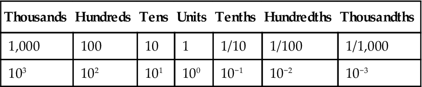
The terms ‘hundreds, tenths’, etc. are simply powers of the base, in this case 10. The binary system works in exactly the same way, but because it uses 2 as its base, rather than 10, its table is slightly different.
Thus, even though the binary system only counts from 0 to 1, if we use a word with enough bits, we can have any number we like (see Table 3.2).
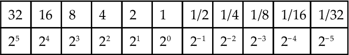
Precision
Computers use binary numbers, so if we make our numerical measurement more precise by using smaller quantising levels, there must be more of them, and a binary word comprising more bits is required. CD used a 16-bit word, and because there are two possible states for each bit, the total number of different levels that can be described by a 16 bit word is 216=65,536. Similarly, a 24 bit system can describe 224=16,777,216 different levels, but requires one-and-a-half times as much memory to store each word (24/16=1½).
As a rule of thumb (ignoring dither), the Dynamic Range (DR) of a digital system is:
where n=number of bits.
Thus, a 16 bit system has a theoretical dynamic range of 6×16=96 dB and a 24 bit system 144 dB (never achieved because Analogue to Digital Convertors (ADCs) simply aren’t that good).
We could decide to be more precise by making more numerical measurements. Sampling twice as often doubles the memory required.
To sum up, a more precise description generates more data, requiring more memory, and this will become significant later.
The Fast Fourier Transform (FFT)
The reason for converting our analogue signal to a digital signal was to allow mathematical techniques to be applied to the resulting numbers and allow patterns to be seen. (Humans are good at recognising patterns, so any technique that reveals patterns helps understanding.) An oscilloscope allows us to spot patterns that repeat in time, such as a spike that occurs each time a sine wave changes polarity, but a spectrum analyser allows us to spot patterns in frequency, perhaps a small spike that indicates fifth harmonic distortion.
The FFT is a mathematical tool that converts data initially presented as a graph of a parameter plotted against time into that parameter plotted against frequency. The FFT is immensely powerful, but it has its limitations.
The Periodicity Assumption
In converting from time to the frequency domain, the mathematics of the FFT makes the assumption that the waveform to be analysed repeats itself periodically. This assumption may seem trivial, but it has major repercussions.
If we capture a single cycle of the waveform, and draw it around a circular drum (like an old-fashioned seismograph) such that the end of the cycle just meets the beginning, then by rotating the drum we can replay the waveform ad finitum and reproduce our original signal. Unfortunately, any uncertainty as to the precise timing of the end of the cycle causes a step in level when we attempt to loop the recorded cycle back to itself on replay. However, if we capture more cycles on our drum, the glitch occurs proportionately less frequently and causes less of an error. Thus, capturing 1,000 cycles reduces the error by a factor of 1,000, but multiplies the length of the waveform record by the same amount.
Windowing
Another way of reducing the step is to force periodicity by applying a window to the waveform record. In this context, a window is a variable weighting factor that multiplies the values of the samples at the ends of the waveform record by zero, but applies a greater weighting (≤1) to samples towards the middle. Since any number multiplied by zero is zero, this forces the end samples to zero and allows the waveform record to repeat without glitches (see Figure 3.4).
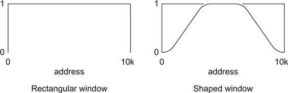
If windowing distorts the waveform record, it must distort the results of the FFT. Windowing either spills energy from high-amplitude bins into adjacent bins, which produces visible skirts around frequencies having high amplitude, or changes bin amplitudes. (Because the process of sampling broke time into discrete slices, the results of an FFT must produce frequencies in discrete slices, and these are known as bins.) All windows are, therefore, a compromise between frequency and amplitude resolution.
A window that does not modify sample values is known as a rectangular window (because it multiplies by a constant value of 1 over the entire waveform record). Because the rectangular window does not modify sample values, it does not cause spreading between bins, and offers the best frequency resolution, but any periodicity violation causes amplitude errors. FFT software generally offers user-selectable windowing, such as Blackman–Harris, which shapes the ends of the waveform record to avoid periodicity violation and minimise consequent amplitude errors at the expense of spreading between frequency bins. Alternatively, Hamming or Hanning windows improve frequency resolution (reduced bin spreading) at the expense of increased amplitude errors.
Best results are obtained by synchronising the oscillator to the FFT system so that only complete cycles without periodicity errors are captured in the record, allowing a rectangular window to be used. If true synchronous FFT is not possible, then a practical compromise is to trigger the analyser from the fundamental frequency and finely adjust oscillator frequency for minimal skirts on the highest amplitude bin.
If multiple waveform records are captured, they can be averaged together to reduce errors. This is a very powerful technique, although it slows measurement speed.
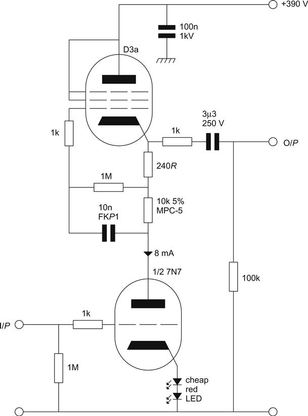
How the Author’s Distortion Measurements Were Made
An MJS401D analogue audio test set and a Tektronix TDS3032 oscilloscope with FFT option were used in combination.
Distortion measurements were made at 1 kHz, and a 400 Hz 36 dB/octave high-pass filter was engaged to reject hum. The meter used an RMS rectifier to sum harmonic amplitudes correctly, and its bandwidth was restricted to the audible range by a 22 kHz 36 dB/octave low-pass filter. The distortion residual was then passed to the spectrum analyser.
The 9 bit oscilloscope/spectrum analyser used a sample rate of 50 kS/s to maximise the number of cycles captured, and the 22 kHz filter in the MJS401D formed the anti-aliasing filter. The oscilloscope was triggered from the 1 kHz fundamental, and rectangular windowing was used, with the MJS401D oscillator frequency fine-tuned for minimum skirts to give quasi-synchronous FFT. To reduce the contribution of random noise, the FFTs were averaged over 16 records (12 dB noise reduction), each 10 kbits long, resulting in >50 dB of reliable spectrum analyser dynamic range.
Because the dynamic range of the audio test set is added to that of the spectrum analyser, the main limitation becomes the distortion residual of the test set, and figures below −90 dB should be viewed with caution.
Now that the distortion measurement method is understood, we can use it as necessary to test and compare low-distortion valve circuits.
Designing for Low Distortion
There are many ways of reducing distortion, or to put it less charitably, it’s easy to generate distortion inadvertently. To simplify investigation, we will consider the distortion generated by a single stage before progressing to multiple stages. We will consider:
We will investigate each aspect in turn and test our hypotheses with practical measurements.
Signal Amplitude
In theory, the distortion generated by triodes is predominantly second harmonic (H2). A common-cathode amplifier using 417A/5842 was set up to test the theory (see Figure 3.5).
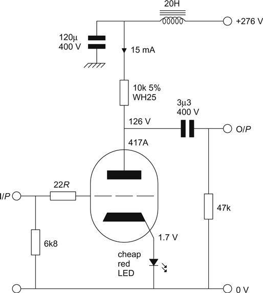
Twenty-two 417A/5842s were tested at an output level of +18 dBu (6.16 VRMS); their results were averaged and are presented in Table 3.3.
Table 3.3
Average Level of Distortion Harmonics Produced by 417-A Common-Cathode Amplifier at +18 dBu
| Harmonic | Level (dB) |
| H1 (fundamental) | 0 |
| H2 | −41 |
| H3 | −100 |
| H4 | −95 |
The distortion generated by the 417A/5842 clearly is dominated by H2. The 417A/5842 type turned out to be a particularly good example, but even for the worst valves H2 is more than 20 dB higher than any other harmonic. This is useful because it means that we can use the following formula to estimate distortion when drawing and comparing loadlines on reliable graphs:
The shape of a triode’s transfer characteristic is a simple curve (Ia∝Vgk3/2), so traversing a smaller distance of the curve becomes a closer approximation to a straight line, and there should be less distortion. This hypothesis was tested by a 7N7/D3a μ-follower circuit (see Figure 3.6).
In order that the test circuit should not be falsely good when approaching grid current, it was driven from a source resistance of 64 kΩ, thus replicating typical conditions of use. The upper limit of measurement was set by the onset of grid current at an output of +34 dBu (THD+N=−43 dB). The lower limit of reliable measurement was set by the ability of the analogue analyser to lock cleanly to the distortion waveform, which began to degrade at an output of +14 dBu (THD+N=−63.5 dB). Between these limits, the output level was changed in 1-dB steps, and a graph of THD+N was plotted against output level (see Figure 3.7).
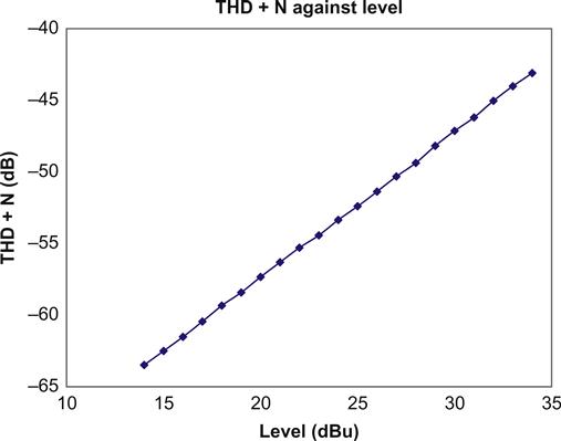
The graph clearly shows that THD+N is directly proportional to output level. Thus, a distortion measurement of 1% at 15 VRMS implies distortion of 0.1% at 1.5 VRMS. This observation is extremely useful if it is necessary to estimate the distortion of a triode handling small-signal voltages – such as would normally be encountered early in an RIAA stage.
The supposition that triode distortion is predominantly H2 and is proportional to level is true for all triodes when used with practical resistive anode loads. The effect of an active load (RL⇒∞) is to minimise H2, but barely changes higher harmonics. Once H2 has been minimised, the effects of the higher harmonics become more significant, with the result that some triodes do not then have distortion that is proportional to level. If you use an active load, you may need to check whether distortion remains proportional to level for that particular type of valve.
Cascodes and Distortion
The cascode is an ideal small-signal RF circuit. It works by placing two devices in series across the high tension (HT) so that the upper device provides most of the gain and loads the lower device with the upper device’s load divided by its voltage gain. This means that the lower device sees a very low resistance load (near vertical loadline), lowering its gain (and in a semiconductor circuit) forcing its voltage gain to unity. From an RF point of view, the reduction of gain in the lower device is extremely advantageous because it reduces Miller capacitance from the output of the device to its input. From an audio point of view, the low impedance load greatly increases H2. Worse, the series connection means that each device has a greatly reduced HT voltage, which tends to increase distortion. For a phono stage, low noise is the primary consideration, so the lower device requires high gm because it reduces noise, but a careful balance of DC current between the upper and lower devices is required to optimise the dynamic range between noise and distortion. However, because distortion is proportional to amplitude, minimising signal amplitude minimises distortion, and the dominant H2 can be removed by cancellation if a pair of cascodes is configured as a differential pair.
Grid Current
Distortion changes with Va and Ia will be investigated later because they are caused by changes in the small-signal parameters μ, ra and gm that are normally assumed to be constant. Thus, unless we also need to maximise voltage swing, our choice of operating point simply needs to be wary of grid current and cut-off. The problems of cut-off are obvious, but grid current causes far more problems.
Distortion due to Grid Current at Contact Potential
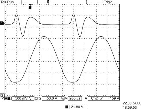
As Vgk approaches 0 V, grid current begins to flow, and the input resistance of the valve falls dramatically. If the source driving the valve had rout=0, this would not be a problem, but it is highly likely that it has significant output resistance, and the potential divider that is momentarily formed at the positive peaks of the waveform where grid current flows clips the input signal. Symmetrical clipping produces a square wave composed of odd harmonics, but grid current clips asymmetrically, so even harmonics can also be expected.
The distortion caused by grid current is obnoxious because it is composed of high-order harmonics. The following traces were obtained by driving the lower valve of a μ-follower into grid current from a source resistance of 47 kΩ. The input signal was increased until distortion of the output waveform was just visible on a carefully focussed analogue oscilloscope. The THD+N was measured to be 2%, and the distortion residual had a very distinctive waveform (see Figure 3.8).
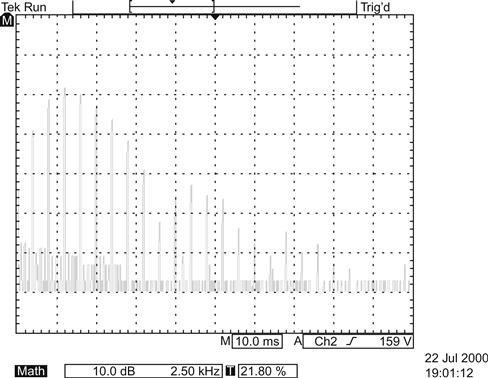
FFT analysis of the distortion residual revealed a spray of high-level, high-order, odd and even harmonics (see Figure 3.9).
Although grid current occurs at Vgk=0 V in an ideal valve, practical valves enter grid current a little earlier due to the thermocouple effect of heated junctions between dissimilar metals within the valve, and the average energy of electrons in the electron cloud above the cathode surface. Typically, grid current begins at Vgk≈−1 V, and this is known as the contact potential. Measuring distortion whilst driving from a high impedance source is an excellent way of determining contact potential for a given valve.
Distortion due to Grid Current and Volume Controls
It is perfectly possible to change the design of the volume control preceding an amplifier stage and measure a change in distortion. The most common type of volume control is a resistor from which a variable tapping is taken, either a wiper moving along the resistive track, or a switch wiper selecting a tapping from a chain of fixed resistors (see Figure 3.10a).
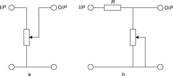
Alternatively, we can use a fixed series resistor followed by a variable shunt resistor (see Figure 3.10b).
Unfortunately, the circuit of Figure 3.10b has much higher output resistance than that of Figure 3.10a. Measuring distortion whilst driving from a high source resistance is a very sensitive test of gas current because the (non-linear) gas current develops a voltage across the source resistance, which is in series with the signal. As the source resistance rises, so does the distortion.
A 6545P cathode follower biassed by an EF184 constant current sink was tested at +20 dBu (7.75 VRMS). When driven from a 5 Ω source, the distortion was 0.02%. A 100 kΩ potential divider volume control has a maximum output resistance of 25 kΩ, so distortion was also measured with a 25 kΩ source resistance, and found to be unchanged. However, when the source resistance was increased to 1 MΩ, the distortion rose to 0.2%. Admittedly, it is unlikely that the source resistance would be as high as 1 MΩ, but 100 kΩ would be quite possible from the volume control in Figure 3.10b.
Operating with Grid Current (Class A2)
Most Class A amplifiers operate without grid current because this allows a high grid resistance that is easily driven. Once Vgk becomes positive, rather than repelling electrons from the cathode, the control grid becomes a weak anode and attracts electrons, most of which are then captured by the true anode that is at a much higher voltage, but some flow out of the grid as grid current. Grid current has important consequences:
• The electron stream from the cathode is divided between grid and anode current, implying partition noise. However, as the most likely use of Class A2 is in the output stage, where signal voltages are high, this noise is unlikely to be a problem.
• There is a potential difference between the grid and the cathode (Vgk) and current flowing through the grid (Ig), so it must be dissipating power in exactly the same way as an anode. If the grid was not designed to dissipate power, it will quickly heat, distorting its shape and possibly destroying the valve.
• Because the input resistance of the grid when operating as an anode is very low, imposing a signal voltage on the grid requires considerable power (P=V2/R), which must be provided by the driver stage.
• However, because the grid is driven positive, it is possible to drive the anode of a triode far closer to 0 V than if Vgk was negative. The efficiency of the output stage is thus significantly increased.
Driver stages for Class A1 are voltage amplifiers that only need to supply sufficient current to charge and discharge the Miller capacitance of the output stage, but a driver stage for Class A2 must provide power. There are two ways in which this power can be delivered.
The driver stage can be designed to be a small power stage. One possible choice is the common-cathode dual triode 6N7 that can be operated either in push–pull or single-ended with the two triodes paralleled to double Pa. A transformer reflects its load impedance by n2, so a step-down transformer with a voltage ratio of 2:1 increases the load impedance seen by the driver valve by a factor of four. Because a transformer in the anode circuit of a valve theoretically allows Va to swing to 2 VHT, requiring double the anode swing is not a problem. Additionally, the low RDC of the secondary reduces the chances of thermal runaway in the output stage. Sadly, good driver transformers are even more difficult to design than output transformers because they operate at higher impedances.
Alternatively, the Class A2 stage can be driven DC-coupled from a cathode follower. A power valve is still required, but it no longer needs to be able to swing many volts. Power frame-grid valves that have high mutual conductance, but low Va(max), such as the 6545P and E55L, are ideal as power cathode followers. Unfortunately, frame-grid valves tend to have modern, efficient heaters (thin heater/cathode insulation), which means that their Vhk(max) is quite low, possibly causing a problem if the Class A2 stage requires significant grid voltage swing. To bias the Class A2 stage correctly, the cathode of the cathode follower can only be slightly positive, but we need a reasonably large value of RL to ensure linearity of the cathode follower, so a negative supply is required (see Figure 3.11).
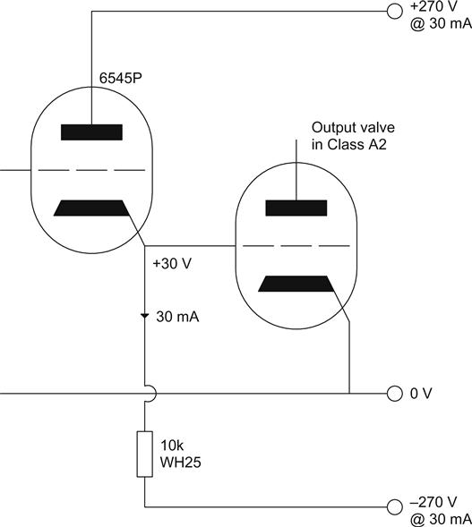
A low output resistance is offered by both of the previous solutions, but it is not zero. Because rout≠0, it forms a potential divider with the input resistance of the Class A2 stage, causing attenuation. If Vgk swings negative, the input impedance of the Class A2 stage becomes infinite, and there is no longer any attenuation, causing distortion. No distortion advantage can be gained using a constant current sink load for the cathode follower because it faces the low-resistance load of the Class A2 grid, but it allows a lower-voltage negative supply, reducing cost. Whereas a Class A1 stage should never be driven into grid current for fear of distortion, the Class A2 stage must never be allowed to stray out of grid current, or distortion will result. Thus, Class A2 power stages typically use high-μ (μ>100) transmitter valves originally intended for Class B use because these valves are designed to pass low anode currents at Vg=0 V even at their intended anode operating voltage.
Distortion Reduction by Parameter Restriction
Triodes produce primarily H2 distortion because as ra changes with Ia, the attenuation of the potential divider formed by ra and RL changes, with more attenuation on one-half cycle of the waveform than on the other. However, there are ways of reducing this distortion:
• Use a large value of RL. If RL>>ra, then the changing attenuation of the potential divider is insignificant because the attenuation itself becomes negligible.
• Hold Ia constant so that ra cannot vary. This implies an active load such as a constant current source is the basis of the μ-follower.
These two methods are actually very similar because both seek to make RL>>ra. (For an ideal constant current source, rslope=∞.) In general, for a given HT voltage and Ia, replacing the load resistor RL with a constant current source can be expected to reduce H2 by a factor of ≈7.
Once the previous methods of distortion reduction have been used, the amplifying valve sees an almost horizontal AC loadline, and when RL>50ra, the far lesser effect of variation of μ with Va becomes observable. The variation of μ with Va can be reduced by avoiding operation at low Ia (where the anode curves begin bunching) and by choosing a valve whose curves bunch less as Ia tends to 0 (see Figure 3.12).
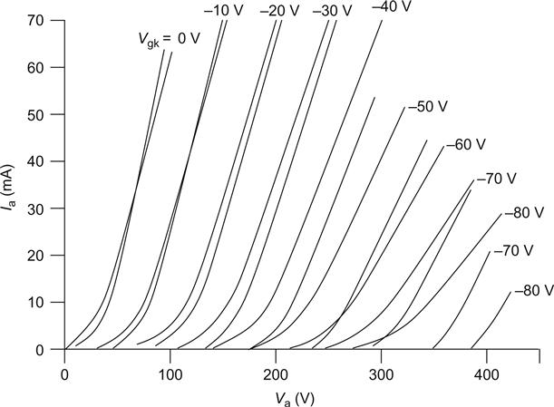
Bunching of anode curves is caused by the inevitable non-uniformity of the electric field between the grid wires at the grid/cathode region, so the graph compares two GEC [2] directly heated triodes having similar μ, but the solid curves are due to a grid wound with a few turns of coarse wire, and the dashed curves are due to a grid wound with more turns of fine wire. Unfortunately, as the grid wire becomes finer, it is less able to support itself, but a frame-grid allows arbitrary thickness of wire, which is why the E88CC, and particularly the 6545P (both frame-grid), exhibit very little bunching.
Alternatively, it may be possible to hold Va constant. Clearly, this cannot be done if the stage has gain, but a cathode follower can be arranged to have constant Ia and Va simultaneously [3] (see Figure 3.13).
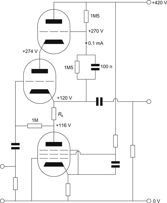
The middle valve is the cathode follower. The lower valve is the traditional pentode constant current sink that forces Ia in the cathode follower to be constant. The upper valve is also a cathode follower and should have high μ and gm, so the 6545P (μ=52) is ideal. The upper valve sees a high impedance load, so its gain is:
The upper cathode follower’s grid is AC coupled to the output of the middle cathode follower, and because its gain is almost unity, its cathode is at the same AC voltage as its grid. Thus, even when the middle cathode follower swings its cathode, the upper cathode follower forces its anode to swing by an almost identical amount, and constant Va has been enforced simultaneously with constant Ia.
Unfortunately, the improvement is accompanied by significant costs:
• The required HT voltage has been raised by Va of the upper cathode follower.
• We need a third elevated heater supply (for the upper cathode follower).
• Cathode followers are already prone to instability, and bootstrapping the anode of one with the output of another invites further problems.
You might have a different opinion, but the author feels that a carefully designed cathode follower sitting on a constant current sink already challenges his test equipment.
Distortion Reduction by Cancellation
In theory, if two common-cathode triode amplifiers are operated in a cascode, because each stage inverts, the distortion of the second triode is inverted with respect to that produced by the first triode, and cancellation should occur. However, a moment’s thought shows that this is unlikely to occur to any significant degree. Distortion is proportional to level, and because the second triode has gain, it produces a significantly higher level, and therefore proportionately higher distortion, than the first triode. A small amount of cancellation may occur, but the improvement is ∝1/A2, so if the second triode was a type 76 (μ=13) and Av=10, we might reduce distortion from 1% to 0.9%, which is less than the sample-to-sample variation of distortion in either valve.
Perhaps we could choose the second valve to be much more linear than the first so that both produce equal amounts of distortion. Low-μ valves are the most linear, so an 845 (μ=5.3) should achieve Av=4, and therefore we need a valve that produces four times the distortion of the 845. This can probably be done, and adjusting the bias of the first valve would allow complete cancellation to be achieved. However, this cancellation would be critically dependent on the gain of the 845, which is determined by RL, yet RL is a loudspeaker whose impedance changes with frequency. In practice, 6 dB reduction in H2 is feasible.
Surprisingly, it is possible to achieve distortion cancellation between a common cathode stage followed by a cathode follower stage, provided that the common cathode stage has its distortion minimised by a constant current load and the cathode follower has its distortion deliberately increased by an AC load (see Figure 3.14).
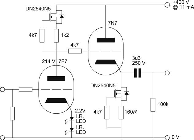
The common-cathode stage produces perhaps 0.1% THD+N, and the dominant harmonic is H2, with all the others better than 20 dB down. In theory, if we could cancel H2, we would be left with only the higher harmonics, and because they are 20 dB further down, our THD+N would have dropped by 20 dB from 0.1% to 0.01%. In practice, the situation is a little more complicated (see Figure 3.15).
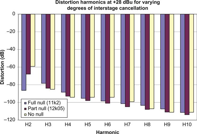
We can see that full nulling (11.2 kΩ AC load) reduces H2 by 27 dB from −59 dB to −86 dB (0.005%), which is certainly impressive, but at the expense of skewing the distortion spectrum so that H3 is 8 dB higher than H2. Note that a 7.5% change in AC load resistance from 11.2 kΩ to 12.05 kΩ radically changes the distortion spectrum. Distortion cancellation can only be achieved reliably if the two valves are identical, carry exactly the same signal and have the same load conditions.
Differential Pair Distortion Cancellation
The differential pair with constant current sink tail provides optimum conditions for distortion cancellation because the signal current is forced to swing between the two valves with no loss. Provided that the load impedances are matched, the voltage swings at each anode must be equal and opposite, theoretically allowing perfect H2 cancellation. The anode load resistors can easily be matched to 0.2% by a DVM, and if each anode drives a cathode follower, then the shunt capacitance is so small that any imbalance is insignificant at audio frequencies. (Even at 20 kHz, Xc=1.6 MΩ for the 5 pF input capacitance of a typical cathode follower, so this is significantly larger than the typical 47 kΩ anode load resistors.)
A Mullard 6SN7GT with well-matched sections was compared in different configurations with Ia=7.5 mA and Va=230 V. Each test circuit was measured at an output level of +14 dBu, but for the differential pair the signal between the anodes was measured (+20 dBu), corresponding to +14 dBu at each anode (see Figure 3.16 and Table 3.4).
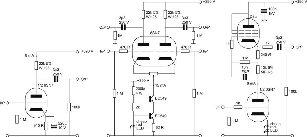
Table 3.4
Comparison of Distortion Harmonics for Different Topologies
| Harmonic | Common cathode (dB) | Differential pair (dB) | μ-Follower (dB) |
| H2 | −51 | −77 | −68 |
| H3 | −93 | −89 | – |
| H4 | (−106) | – | – |
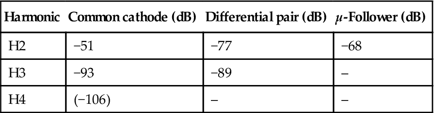
As can be seen from Table 3.4, the differential pair cancels even harmonics, but sums odd ones. Although 0.0035% H3 is unlikely to be a problem, it indicates that differential pairs are ideally built with valves that produce small amounts of odd harmonic distortion. Conversely, the μ-follower was not as effective at reducing H2, but all other harmonics were below the limits of reliable measurement.
Push–Pull Distortion Cancellation
A push–pull transformer-coupled Class A output stage meets most of the requirements for distortion cancellation. In practice, unless the two valves are an accurately gain-matched pair, or provision has been made for DC and AC balance, cancellation cannot be perfect. Nevertheless, 14 dB H2 cancellation is routinely achieved because the tight coupling between the two halves of the transformer assists AC balance.
The Western Electric Harmonic Equaliser
The harmonic equaliser is a recent rediscovery championed by John Atwood and Lynn Olsen. The surprisingly clearly written patent [4] states that distortion reduction action is due to cancellation between H3 produced directly by the valve and that produced by intermodulation between H2 and the fundamental, H1. Remember that intermodulation distortion produces sum and difference frequencies, so H1+H2=H3 as stated by the patent, and H1−H2=−H1, which means that the difference frequency is at the same frequency as the fundamental, but has inverted polarity, thereby slightly attenuating it.
In push–pull form, the equaliser consists of a resistor connected from the two cathodes to ground with its value chosen purely from AC considerations – biassing is a separate issue (see Figure 3.17).
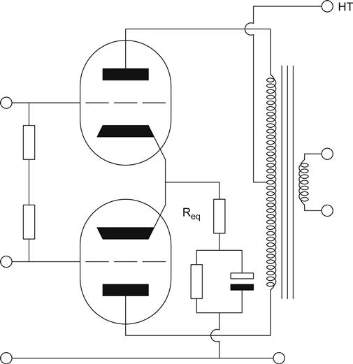
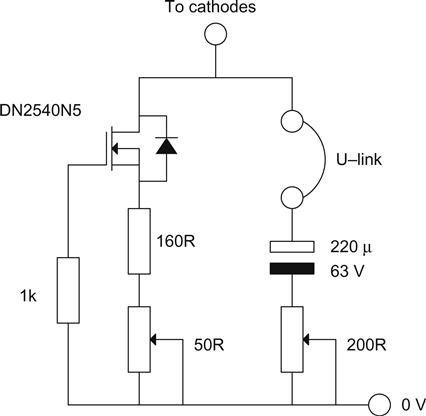
The easiest way to determine the required value of the resistor is to temporarily substitute a constant current sink set to the required DC current and bypass it with a capacitor in series with a variable resistor (the equaliser) (see Figure 3.18).
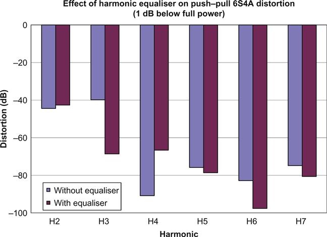
Sadly, the author’s experiments indicate that although the equaliser affects all valves, it isn’t always a positive effect. As a beneficial example, adding a 91 Ω equaliser resistor to a pair of push–pull 6S4As operating with a 9k5a–a load from 320 V reduced H3 by 28 dB so that the spectrum became dominated by H2, with H3 and all others >20 dB below that (see Figure 3.19).
Side-Effects of the Harmonic Equaliser
Although in a harmonic equaliser resistor simple addition can significantly improve an output stage’s distortion spectrum, it does so by cancellation, and that always means that it will be sensitive to load resistance. Once the value of the harmonic equaliser resistor has been set, load resistance must not change (see Figure 3.20).
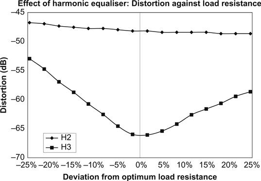
As can be seen, the load resistance ideally needs to be within ±5% of nominal to achieve the full benefit of the harmonic equaliser.
Unfortunately, the impedance of a moving coil loudspeaker rises with frequency due to voice coil inductance and has a low frequency electrical resonance that looks like an inductor and a capacitor in parallel due to the mechanical resonance formed by the mass of the cone and compliance of the suspension. In order for an output stage’s harmonic equaliser to work correctly, the amplifier must be connected directly to a single resistive loudspeaker and the harmonic equaliser resistor must be set to match that specific loudspeaker. Fortunately, most moving-coil loudspeakers can be rendered adequately resistive above resonance by the addition of an appropriate Zobel network across their terminals (see Figure 3.21).
Unfortunately, applying the harmonic equaliser tends to increase the output resistance of the output stage. The significance of this increased output resistance is that the loudspeaker system must be designed to be driven by this specific non-zero output resistance.
In short, an amplifier having an output stage using the harmonic equaliser technique cannot be used as a universal amplifier. Whether it is part of a complex loudspeaker system employing an active crossover or a loudspeaker with a single full-range driver, it is a complementary system where the amplifier must be designed for a specific loudspeaker, and the loudspeaker’s acoustic loading must be designed with the specific amplifier in mind. It is probably the combination of these requirements that has prevented widespread adoption of the harmonic equaliser, yet the requirements can be met, as we will see in Chapter 6.
Although an explicit harmonic equaliser might not have been intended, cathode feedback sometimes results in distortion reduction exceeding the feedback factor, implying cancellation and consequent load sensitivity. For both amplifiers, cathode feedback in the Quad II power amplifier and in the author’s ‘Scrapbox Challenge’ produced better results than expected from the feedback factor alone, implying cancellation.
DC Bias Problems
Having chosen the topology of a stage with great care, we choose an operating point that cunningly maximises output swing, minimises distortion, uses standard component values, and all within the current capability of the power supply. We now need to bias the stage, which can be done in a number of ways:
Cathode Resistor Bias
Bias can be achieved by inserting a resistor in the cathode path (see Figure 3.22).
If valve current rises, resistor current also rises, making the cathode more positive with respect to the grid, thus tending to turn the valve off and offering some overcurrent protection. This method of bias has the least sensitivity to variations between valves, making it by far the most popular bias choice. We know Ia and the required Vgk, so we simply apply Ohm’s law to determine the required cathode resistor.
However, inserting a resistance in the cathode circuit of a single valve common-cathode amplifier creates negative feedback that reduces gain, which might not be acceptable. The traditional solution bypasses the resistor with a capacitor (which is a short circuit at audio frequencies), the cathode is connected to ground at AC, and negative feedback is prevented. It is generally argued that the audio bandwidth extends from 20 Hz to 20 kHz, and that audio electronics should be as nearly perfect as possible within this bandwidth. Because rk tends to be low (typically <500 Ω), the cathode bypass capacitor needs to be quite a high value, forcing it to be an electrolytic type. Unfortunately, such a capacitor is typically +25%, −15% tolerance so this haphazard time constant should not be allowed to affect any formal filtering action, and its value is usually set to produce f−3 dB=1 Hz, which is the same as saying τ≈160 ms.
When biassing a stage, we make the assumption that the signal voltage is sufficiently small that it does not affect the DC conditions. However, as clipping is approached, the signal voltage at the anode of a triode could be hundreds of volts peak to peak, and the distortion (which contains a DC component) temporarily lowers the average Va. A secondary effect of this distortion is that it has a DC component that changes the mean anode current.
As an example, a common-cathode triode amplifier was tested. When the generator was muted, Va=117.1 V, but when the stage was driven to a level that produced 5% THD+N, the mean anode voltage fell to 114.2 V, indicating a change in mean anode current. Since this anode current flows through the cathode-bias resistor (which is in parallel with the cathode capacitor), any change in mean anode current is integrated by the cathode CR network (τ≈160 ms). When the overload passes, the capacitor takes 5τ≈1 s to recover to 99% of the previous bias point. During this time, ra (which is dependent on Ia) will change, slightly changing rout. If the circuit feeds a passive equalisation network, rout is inevitably part of the design, so the change in rout causes a temporary frequency response error. Although a minor frequency response error could be considered irrelevant when the amplifier is producing 5% THD+N, a frequency response error that decays to zero over a period of 1 s after overload might not be so acceptable.
The bias shift effect can be observed by monitoring the DC voltage across the cathode bypass capacitor with and without a large sine wave at the anode. This method has the advantage that an ordinary DVM can be used, whereas measuring at the anode requires an instrument that can measure DC accurately in the presence of significant AC.
Ideally, there should never be a shift in the operating point of a valve, whatever the signal level. Provided that the valve is never driven to produce >1% THD, cathode bias is perfectly satisfactory, but if clipping is likely, an alternative bias strategy should be considered.
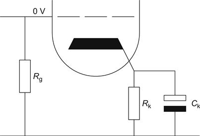
Grid Bias (Rk=0)
If Rk=0, the DC component of distortion cannot cause bias shift.
Grid bias from an auxiliary low current negative supply is common in the output stages of Class AB power amplifiers, whereas battery bias is occasionally found in pre-amplifiers (see Figure 3.23).
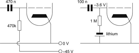
Note that battery bias can be applied either in series or in parallel. In practice, parallel is usually preferred because the output impedance of the previous stage and the battery’s series resistor form a potential divider that attenuates battery noise, whereas there is no attenuation of battery noise in series mode.
Grid voltage is fixed, and valve current is determined purely by valve characteristics, so there is no protection against overcurrent, or compensation for changes in valve characteristics with age.
Overcurrent protection is important in transformer coupled stages because the winding resistance of the transformer is negligible and an output valve is almost certainly being operated at maximum anode dissipation. Current from the supply is, therefore, almost unlimited, and a fault is likely to damage an expensive valve quickly, and worse, risks the even more expensive output transformer.
Conversely, in pre-amplifiers or driver stages using resistive or active loads, the valve is typically operated at less than half maximum anode dissipation, and the anode load limits fault current. It is quite conceivable that a fault resulting in maximum current could leave the valve operating well within its limits, and no damage at all would occur.
Rechargeable Battery Cathode Bias (rk=0)
Rechargeable cells have extremely low internal resistance, so if they are inserted in the cathode path, they do not allow a feedback voltage to appear (see Figure 3.24).
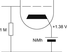
Although the diagram shows only one cell, a number of (identical) cells could be connected in series to set the required voltage, although this could become rather bulky. Provided that Ik≤C/10 (C is the cell capacity in A h), the self-heating caused by continuous charging will not damage the cell. However, since the cell is in a valve amplifier, it is probably rather warmer than the battery manufacturer expected, so limiting the current to C/20 might be wise. An AA-size nickel metal hydride (NiMH) cell develops ≈1.38 V when charged continuously at 15 mA.
Diode Cathode Bias (rk≈0)
Rather than using a resistor, we can use a diode for cathode bias (see Figure 3.25).
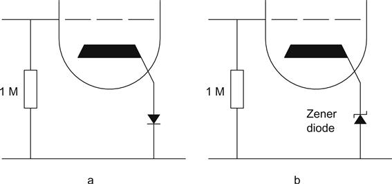
The advantage is that a diode’s slope (AC) resistance is so much lower than the traditional cathode resistor that we no longer need to bypass it with a capacitor. Although diode slope resistance is low, sometimes it may be necessary to calculate its effect on ra. Table 3.5 compares forward drops and slope resistances (rslope) for various diodes.
Table 3.5
Comparison of Forward Drops and Slope Resistances of Various Diodes
| Diode type | Forward drop at 10 mA (V) | Typical rslope at 10 mA (Ω) | Pure R at 10 mA (Ω) | R/r |
| Silicon (1N4148) | 0.75 | 6.0 | 75 | 13 |
| Germanium (OA91) | 1.0 | 59 | 100 | 1.7 |
| Infrared LED (950 nm) | 1.2 | 5.4 | 120 | 22 |
| Cheap inefficient red LED | 1.7 | 4.3 | 170 | 40 |
| HLMP6000 red LED | 1.63 | 3.8 | 163 | 43 |
| Cheap yellow/green LED | 2.0 | 10 | 200 | 20 |
| EZ81 | 2.3 | 195 | 230 | 1.18 |
| True green LED (525 nm) | 3.6 | 30 | 360 | 12 |
| Blue LED (426 nm) | 3.7 | 26 | 370 | 14 |
| EZ80 | 5.5 | 485 | 550 | 1.13 |
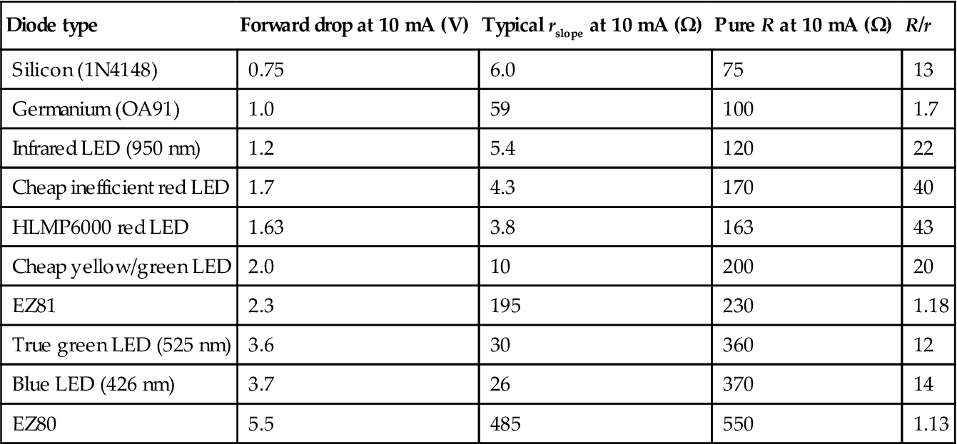
The column ‘Pure R’ is the value required to achieve the diode forward voltage using a resistor. Thus, the column ‘R/r’ is the ratio by which the diode improves upon a pure resistance – and the larger the number, the better.
The thermionic and germanium diodes barely improve on a pure resistance, so they can be discounted immediately. The winner is the red LED, but it needs to be one of the older less efficient designs that you might find cheap in a junk shop, rather than a modern high brightness type. Alternatively, the more modern (and more readily available) Agilent HLMP6000 LED is slightly better and this red LED is so good that if higher voltages are needed it is better to use a series string of red LEDs than a single, inferior colour LED.
As an example, suppose we needed 3.4 V. Referring to Table 3.5, we see that we could approximate it with a true green LED (3.6 V and 30 Ω) or a pair of HLMP6000s (3.26 V and 7.6 Ω) – the slope resistance of the two red LEDs is a quarter that of the single green LED.
As mentioned in Chapter 1, the author’s measurements show that over a range of 0.3–10 mA, the forward drop of a typical HLMP6000 may be predicted from:
Differentiating, the slope resistance is:
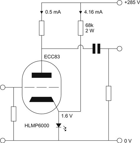
This equation is significant not so much because it allows us to estimate a value for rslope, but because it shows that rslope is inversely proportional to IDC, suggesting that LED bias is best suited in stages passing 5 mA. Nevertheless, it is possible to use LED bias in low current stages if additional current is passed through the LED, perhaps from a resistor connected to the HT, or from a constant current source to a lower voltage source. In this way, an ECC83 requiring 1.6 V but only passing 0.5 mA could be biassed by inserting an HLMP6000 in its cathode circuit and driving additional current through the LED. For a typical HLMP6000 red LED, the current needed to develop the required 1.6 V forward voltage can be found using:
We already have 0.5 mA from the ECC83, so we need an extra 4.16 mA from somewhere else. If we had a 285 V HT, then a 68 kΩ resistor would do, but it would dissipate 1.2 W, so a 4 W component would be needed. Nevertheless, when the choice is between a 3.2 kΩ cathode-bias resistor (needing a bypass capacitor) and an LED with a slope resistance of 5.7 Ω that doesn’t need to be bypassed, then that 68 kΩ 4 W resistor suddenly starts making a lot more sense (see Figure 3.26).
Reverse bias generally produces more noise in a diode than forward bias, but enables higher reference voltages. Low voltage Zener diodes truly use Zener action, whereas higher voltage diodes actually use the avalanche effect. At 6.2 V, both effects are present, their opposing temperature coefficients cancel and rslope is at a minimum, so 6.2 V Zeners are the most stable. If a stable high voltage reference is required, it is usually better to have a string of 6.2 V Zeners than a single high voltage Zener.
From a DC point of view, diode bias is ideal for the lower valve of a μ-follower or SRPP because Ia is stabilised by the bias arrangements of the upper valve.
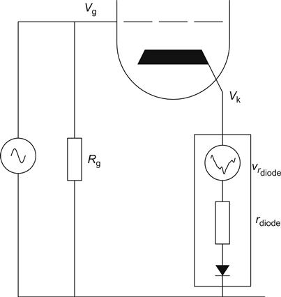
Because rslope≠0, a change in signal current causes a change in the voltage across the diode. The signal current also produces the voltage across RL, so:
Cross-multiplying:
The significance of this equation is that we have just seen that rslope is inversely proportional to applied current, and because rslope varies with signal current, the signal voltage developed across it must be distorted. Unfortunately, this distorted signal voltage is in series with the input signal because the valve amplifies the difference in voltage between the grid and the cathode (see Figure 3.27).
However, the equation and the diode curve show us that the distortion added by the diode can be reduced by:
• Avoiding diode bias for Idiode<5 mA (because rslope is particularly variable at low currents).
These conditions imply that diode bias is best suited to:
• RIAA input stages: Ia is high and signal levels are low. Additionally, the stage can recover instantly from clipping due to high voltages at high frequencies caused by dust, etc., on the record.
• μ-Follower stages: The active load maximises RL, and Ia is likely to be high (minimising the variation in rslope).
Constant Current Sink Bias
A constant current sink allows cathode current to be forced to the design value despite valve parameters. However, because a constant current sink is an open circuit to AC, it would cause 100% negative feedback in a single-ended stage, so it must be bypassed with a capacitor (see Figure 3.28).
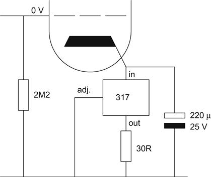
Once bypassed by the capacitor, the AC performance of the constant current sink becomes irrelevant, so a three-terminal regulator such as the 317 becomes perfectly acceptable, and this strategy is quite popular in output-valve cathodes. This is a very rare occasion when DC accuracy is more important than AC performance because accurate matching of DC currents in a push–pull output stage enables us to eliminate the magnetising current that would cause a toroidal output transformer’s core to saturate and generate bass distortion. Note also that because the cathode current has been forced by the 317 CCS (and therefore cannot run away), the grid-leak resistor can become rather larger than the maximum specified by the valve datasheet, enabling a smaller coupling capacitor from the preceding stage.
Differential pairs and cathode followers require exemplary AC performance, and DC accuracy is generally a secondary consideration, which was why we took such care when investigating their design at the end of Chapter 2.
Individual Valve Choice
Although a set of anode characteristics having noticeably different spacings between the curves indicates distortion, evenly spaced characteristics do not guarantee low distortion. Ultimately, we must either use valves designed for low distortion, or test valves for distortion.
Which Valves Were Explicitly Designed to be Low Distortion?
Minimising distortion costs money, so when low-distortion valves were designed, they were targeted specifically at the audio market, which included the broadcast, recording and film industries and, of course, the consumer.
In the 1930s, gain was extremely expensive. The idea of deliberately throwing gain away (negative feedback) was treated as heresy, so much so that although Black’s jotted notes were witnessed on 18 August 1927, his US patent [5] was not issued until 21 December 1937. As a consequence, low distortion was reliant on valve design and construction, so valves like the 76 were designed to be low distortion. As feedback became more widely accepted, it became cheaper to reduce distortion by sacrificing gain, so the final generation of valves had higher gain, but low distortion became less important.
Low-distortion valves were also required by the telecommunications companies, but not because they were concerned with the fidelity of baseband audio. If we need to provide 1,000 analogue telephone circuits between two cities 10 miles apart, we could lay 1,000 twisted pairs, but a cable containing this amount of wire is expensive and cumbersome to lay. The solution adopted by the telecommunications companies was to modulate each telephone circuit onto an RF carrier with its own frequency – just like different radio stations. One thousand modulated carriers could then be passed down a single (usually coaxial) cable which was cheap and easily laid. All cables introduce loss, and between cities the loss becomes significant, so each cable needed repeater amplifiers at regular distances. One of the many advantages of multiplexing 1,000 telephone circuits onto one cable was that only one repeater amplifier was needed every few miles instead of 1,000, reducing cost. However, any distortion in that amplifier would cause one telephone conversation to crosstalk onto another. Valves designed for use in broadband telephone repeater amplifiers were therefore required to produce low distortion.
Many of the final generation of valves used a frame-grid, and some, such as the 417A/5842, were explicitly designed for low distortion. Other valves such as the ECC88/E88CC simply benefited from improved production engineering and produce usefully low distortion. Some valves such as the E182CC and 6350 were designed for use in early digital computers, where the most important consideration was long life even with full heater power and no anode current, which tempts the growth of cathode interface resistance.
Finally, some valves were designed and manufactured with a complete lack of regard for distortion.
The problem of field, or vertical, scanning in a television using a Cathode Ray Tube (CRT) was very similar to that of an audio amplifier driving a loudspeaker. Both use a transformer to couple to the driving valve, and the frequency range is similar. However, CRT scan coils must be driven by a controlled current, rather than applied voltage as is conventional for loudspeakers. Unfortunately, the finite (and changing) primary inductance Lp of the small iron-cored output transformer drew a current in addition to the scan coil current, and this meant that the current waveform drawn from the field scan valve was distorted compared with the ideal current required by the scan coils. There were many ways of achieving a compensating distortion, but one was to use the curvature of the Ia/Va characteristic of a triode. Since transformer Lp was not tightly controlled, the required distortion had to be controllable, so a variable resistor was often inserted in the cathode circuit of the valve to allow adjustment of vertical display linearity.
The crux of the previous argument is that there was no requirement whatsoever for the valve manufacturers to produce field scan valves with outstanding or even consistent linearity, since this had to be individually adjusted for each television’s CRT. Early field scan valves such as the dual triode 6BX7 show wide variations in distortion (4:1 between best and worst), so they have to be selected for audio use, and the probability of finding a pair of low-distortion valves in one envelope is low, so selecting a pair of low-distortion 6AH4 single triodes would be a much cheaper alternative. Later generation valves such as the ECC82 (also intended for use as a field scan oscillator) benefited from improved production techniques and distortion is extremely consistent from sample to sample; it is consistently poor.
Carbonising of Envelopes
Deketh [6] pointed out that not all electrons accelerated from the cathode/grid interface strike the anode – some miss and collide with the envelope, causing secondary emission. Secondary emission is important because it means that the envelope acquires a negative charge that can distort the flight of electrons from cathode to anode. Deketh considered distortion at high amplitudes in power valves and showed that carbonising the inside surface of the envelope was beneficial because it reduced secondary emission. At the time, nobody was worried about audio distortion at <1%, and Deketh might not have had access to an audio spectrum analyser, so he did not publish distortion results at lower levels. Nevertheless, this author’s measurements at +28 dBu (≈19.5 VRMS) show significantly reduced (≈−6 dB) distortion for samples of the 6SN7 having a carbonised envelope compared to clear envelopes.
Deflecting Electrons
Amplifying valves control the flight of electrons by imposing electric fields, but electrons can be deflected by magnetic fields. The Earth’s magnetic field is quite weak, so it is unlikely that orienting a valve in any particular direction will affect distortion, but most sheet electrodes are made of nickel, which can easily be magnetised. If the valve was constructed from concentric cylindrical electrodes, magnetic deflection would not matter unless it caused electrons to miss the anode, but box constructions do not have radial symmetry, so horizontal magnetic deflection could influence anode current.
Beam tetrodes with aligned grids are the most susceptible to magnetic fields because vertical magnetic deflection could cause the sheets of electrons to intercept g2 rather than passing cleanly between the vertically aligned windings. Thus, a magnetic field can change the Ia/Ig2 ratio, and it would be foolish to suggest that this could not affect distortion. Some years ago, using a coil intended for degaussing television display tubes, the author jokingly degaussed the KT88 (aligned grid beam tetrodes) of a power amplifier, and everyone heard a slight difference.
We should be aware that degaussing requires the magnetic material to be taken to saturation in both directions and then gently taken through ever decreasing hysteresis loops until the residual magnetism is zero. Thus, magnetisation and demagnetisation are achieved by brute force – the author’s degaussing coil is 10″ (250 mm) in diameter, consumes 750 VA and is rated only for intermittent use. Applying an audio signal to an amplifier cannot possibly achieve this effect, no matter how exotic the signal may be.
Testing to Find Low-Distortion Valves
Low-noise input stages demand high gm, and signal levels are so low that distortion is not an issue. To minimise noise, well-designed circuitry amplifies low-level signals once only, and thereafter carries line-level signals.
When designing a power stage, the most important consideration is Pa(max), and the consequent DC requirements force distortion to be quite low down on the list of priorities. Further, power stages are used once only to drive the load.
Because of the previous two arguments, low distortion valves are essential for line-level processing (because there is likely to be so much of it), but they need not have outstanding gm or Pa(max). High μ valves might be undesirable if their design assumed the use of negative feedback to reduce distortion. Sadly, most of the low-μ valves were designed for television field scan, so their distortion is distinctly questionable unless individually selected. The remaining valves are medium-μ and have Pa(max)<5 W.
The 6SN7 is widely accepted as a low-distortion valve, but how well does it justify its reputation? Bearing in mind that valves were assembled by hand and subject to wide production tolerances, is there a ‘best’ medium-μ valve or manufacturer? This section seeks to answer these questions by reporting on the testing of a selection of medium-μ valves under identical conditions.
The Test Circuit
If we require a low-distortion gain stage, this can be achieved by a single-ended stage with an active load, or a differential pair with resistive loads and constant current sink tail. In short, circuit design can reduce distortion, but only to the point where the valve’s irreducible distortion takes effect. If we are to select valves for minimum distortion, we should focus on their irreducible distortion, since higher levels of distortion can always be reduced by suitable circuit design. Although this complicates matters by requiring us to measure distortion in a stage deliberately designed for low distortion, it has the benefit of enforcing a level playing field.
If we later use a topology that does not minimise distortion, and valve ‘A’ sounds better than valve ‘B’, it is because valve ‘A’ suits the topology better than valve ‘B’, not because valve ‘A’ is ‘better’ than valve ‘B’.
As previously mentioned, distortion in a triode amplifier is dominated by the variation of ra with Ia. Provided that RL>>ra, the variation of ra is insignificant, so distortion can be reduced by maximising RL. In addition, the valve should pass sufficient anode current to place its operating point well clear of the typical bunching of anode curves experienced at low currents. Accordingly, the valves were tested in a μ-follower circuit passing ≈8 mA anode current. In this configuration, the test valve sees RL≈800 kΩ, which although far from infinite, can be put into perspective by realising that if a true 800 kΩ resistor were to be substituted, a 6.4 kV HT supply would be required. Heater filaments were fed from a stabilised DC supply adjusted for the correct voltage at the heater pins (see Figure 3.29).
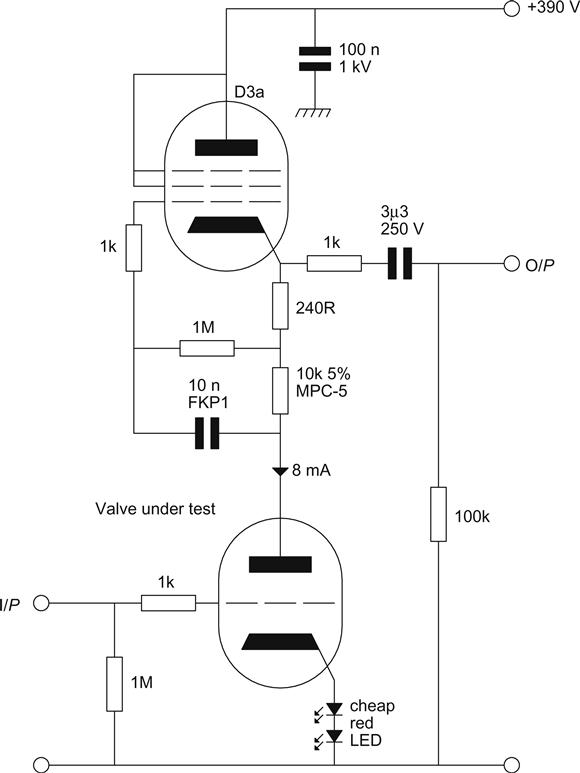
Audio Test Level and Frequency
Since distortion was expected to be low, the valves had to be tested at a sufficiently high output level to make the distortion easily measurable, yet well below clipping. +28 dBu (≈19.5 VRMS) was found to be a good compromise, so each valve had its input level adjusted to produce precisely +28 dBu at its output. Distortion in all the reported valves is directly proportional to level, so distortion at lower levels can be extrapolated from the test data.
Although initially tested at 120 Hz, 1 kHz and 10 kHz, distortion of the test circuit was found to be completely independent of frequency, so the valves were tested at 1 kHz only. For most of the valves, harmonics beyond H6 were too close to the oscillator distortion residual for reliable measurement, so measurement was only attempted on harmonics up to and including H6.
Test Results
All of the valves tested were ‘New Old Stock’ (NOS), so the newest valves were at least 30 years old, and the oldest was 58. Since the valves have been out of production for decades, for some types only a few samples were available to the author.
Raw data from the measurements were analysed in a spreadsheet, and broken into different groups as and when significant differences became apparent.
Table 3.6 summarises the results of the 6SN7GT/12SN7GT and its direct equivalents. The number of samples refers to the number of individual triodes tested, not envelopes.
Table 3.6
Comparison of Distortion Harmonics Within the 6SN7 Family
| Type | Samples | H2 | 1σ | H3 | 1σ | H4 | 1σ |
| 6SN7GT/12SN7GT | 44 | −50 | 3.6 | −85 | 8.4 | −96 | 5.9 |
| 7N7 | 82 | −52 | 3.3 | −85 | 8.6 | −97 | 6.7 |
| 14N7 | 62 | −52 | 3.3 | −85 | 8.6 | −97 | 6.7 |
| Carbonised 6SN7GT | 6 | −54 | 1.8 | −94 | 5.6 | – | |
| Carbonised CV1988 | 12 | −57 | 2.6 | −85 | 7.2 | −93 | 4.2 |
| 12SX7GT | 12 | −50 | 1.9 | −83 | 3.2 | −94 | 6.0 |
| GEC/Marconi B36 | 6 | −51 | 2.0 | −90 | 8.1 | −88 | 2.0 |
| 6J5GT (various) | 6 | −50 | 4.1 | −82 | 12.7 | −97 | 3.1 |
| Pinnacle 6J5GT | 138 | −52 | 2.6 | −90 | 6.7 | −96 | 3.9 |
| RCA 6J5 | 15 | −47 | 4.8 | −84 | 8.3 | −89 | 7.7 |
| GEC L63 | 5 | −50 | 1.6 | −86 | 4.4 | −89 | 4.4 |
| 7A4 | 3 | −48 | 0.2 | −73 | 1.6 | −93 | 1.2 |
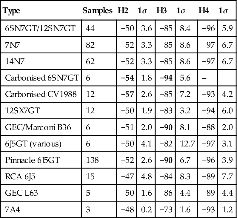
Table 3.7 normalises distortion to the 6SN7GT/12SN7GT to enable clearer comparison.
Table 3.7
Normalised Comparison of Distortion Harmonics Within the 6SN7 Family
| Type | Samples | H2 | H3 | H4 | |||
| dB | Ratio | dB | Ratio | dB | Ratio | ||
| 6SN7GT/12SN7GT | 44 | 0 | 1 | 0 | 1 | 0 | 1 |
| 7N7 | 82 | −2 | 0.79 | 0 | 1 | −1 | 0.89 |
| 14N7 | 62 | −2 | 0.79 | 0 | 1 | −1 | 0.89 |
| Carbonised 6SN7GT | 6 | −4 | 0.63 | −9 | 0.35 | −14 | 0.2 |
| Carbonised CV1988 | 12 | −7 | 0.45 | 0 | 1 | +3 | 1.4 |
| 12SX7GT | 12 | 0 | 1 | +2 | 1.26 | +2 | 1.26 |
| GEC/Marconi B36 | 6 | 0 | 1 | −5 | 0.56 | +8 | 2.5 |
| 6J5GT (various) | 6 | 0 | 1 | +3 | 1.4 | −1 | 0.89 |
| Pinnacle 6J5GT | 138 | −2 | 0.79 | −5 | 0.56 | 0 | 1 |
| RCA 6J5 | 15 | +3 | 1.41 | +1 | 1.12 | +7 | 2.2 |
| GEC L63 | 5 | 0 | 1 | −1 | 0.89 | −3 | 0.71 |
| 7A4 | 3 | +2 | 1.26 | +12 | 4 | +3 | 1.4 |
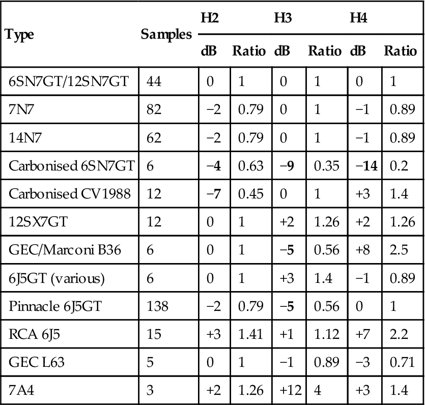
Interpretation
The manufacturers claimed that all the preceding valves were electrically equivalent. Nevertheless, there are significant differences between the valves, and useful conclusions can be drawn from Table 3.7.
• Valves with carbonised glass envelopes produce less distortion. Deketh reported that carbonised envelopes reduced distortion at maximum power, but this series of tests suggests that the improvement is proportional to level, and that carbonised envelopes significantly reduce distortion at lower amplitudes.
• The RCA 6J5 (metal envelope) has significantly higher distortion than the 6J5GT, probably due to increased numbers of gas ions resulting from outgassing of the metal envelope causing increased grid current.
• Despite having a clear envelope, the (Russian-made) Pinnacle 6J5GT offers very low distortion – significantly better than any other manufacturer of 6J5GT.
• The Loktal™ base was specifically designed to reduce stray capacitances and inductances by eliminating the glass pinch required by the Octal base, hence the 6SN7GT/12SN7GT has a claimed Cag≈4 pF, whereas the 7N7 has a claimed Cag=3 pF [7].
• Some valves were selected from the standard production line by their manufacturers. This test shows no significant difference in distortion for the 12SX7 (simply a 12SN7GT selected for transconductance [8] at Va=28 V) compared to the standard 6SN7GT/12SN7GT.
• The third harmonic distortion of the Loktal™ 7A4 single triode is very disappointing, but as only three samples were available for testing, the results are probably not statistically significant even though the standard deviation was only 1.6 dB.
• The *SN7GT family is available with four different heater filament constructions [9], so Table 3.8 compares the different types.
Table 3.8
Heater Voltages and Currents Within the *SN7 Family
| Voltage (V) | Current (mA) | Heating power (W) | |
| 6SN7GT | 6.3 | 600 | 3.78 |
| 8SN7GT | 8.4 | 450 | 3.78 |
| 12SN7GT | 12.6 | 300 | 3.78 |
| 25SN7GT | 25 | 150 | 3.75 |
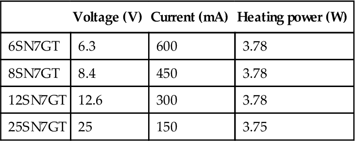
As can be seen from Table 3.8, the heater power is almost identical for all types. Physically, the 6SN7GT has its heaters wired internally in parallel, whereas the 12SN7GT sometimes has them wired in series, but electrode construction is identical, so distortion ought to be similar, so Table 3.9 compares distortion of the 6SN7GT with that of the 12SN7GT.
Table 3.9
Comparison of Distortion Harmonics Between 6SN7 and 12SN7
| Samples | H2 | 1σ | H3 | 1σ | H4 | 1σ | |
| 6SN7GT | 28 | −50 | 3.5 | −83 | 8.9 | −96 | 5.7 |
| 12SN7GT | 16 | −51 | 3.8 | −87 | 7.3 | −97 | 6.5 |
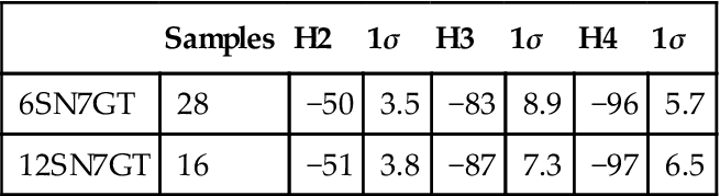
The two valves are very similar – the differences are well within the margins of uncertainty.
Similarly, we can compare the 7N7 with the 14N7 (Table 3.10).
Table 3.10
Heater Voltages and Current Within the Loctal Family
| Voltage (V) | Current (mA) | Heating power (W) | |
| 7N7 | 6.3 | 600 | 3.78 |
| 14N7 | 12.6 | 300 | 3.78 |

Again, we would expect the distortion between the two types to be similar (Table 3.11).
Table 3.11
Comparison of Distortion Harmonics Between 7N7 and 14N7
| Samples | H2 | 1σ | H3 | 1σ | H4 | 1σ | |
| 7N7 | 82 | −52 | 3.3 | −85 | 8.6 | −97 | 6.7 |
| 14N7 | 62 | −52 | 2.4 | −88 | 7.8 | −95 | 6.4 |
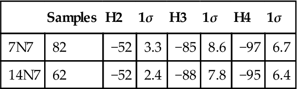
Summarising, the differences between valves having different heater voltages are well within the margins of uncertainty. This is good news because it means that we don’t have to use the expensive 6.3 V heater valves, but can use the cheaper and more plentiful 12.6 V heater valves and enjoy the reduction in electromagnetic hum caused by their reduced heater current, although the higher heater voltage causes commensurately more electrostatic hum. The significance of trading electromagnetic hum for electrostatic hum is that although both types can be shielded, earthed aluminium cooking foil is an effective electrostatic shield, whereas effective electromagnetic shielding requires a far greater thickness of iron or expensive mu-metal. Naturally, both problems disappear if we use regulated DC heaters.
A Convention
The author has adopted a convention that will be applied throughout this book. Having established that the 6J5GT, 6SN7GT, 12SN7GT, 7N7 and 14N7 are electrically virtually identical, and that the 8SN7GT and 25SN7GT can be expected to be similar, economy of nomenclature is necessary. From now on, this family will be called the *SN7/*N7 family (to distinguish between the bases and capacitances). Please note that the 6N7 is a completely different beast, and bears no relation to a 7N7.
Alternative Medium-μ Valves
Table 3.12 shows possible alternatives to the *SN7/*N7 family.
Table 3.12
Electrical Alternatives to the *SN7/*N7 Family
| Type | μ | Samples | H2 | 1σ | H3 | 1σ | H4 | 1σ | H5 | 1σ | H6 | 1σ |
| 7AF7 | 16 | 4 | −38 | 0.3 | −62 | 1.5 | −74 | 0.6 | −89 | 4.2 | −91 | 5.7 |
| ECC82/12AU7/B329 | 18 | 28 | −37 | −56 | 1.4 | −73 | 3.9 | −86 | 6.6 | −96 | 3.1 | |
| E182CC/7199 | 18 | 30 | −45 | 1.7 | −70 | 1.5 | −92 | 3.7 | ||||
| E288CC | 20 | 14 | −49 | 1.3 | −69 | 0.9 | −89 | 5.4 | −95 | 7.2 | −96 | 4.9 |
| 37 | 9 | 9 | −45 | 0.6 | −69 | 4.9 | −87 | 5.7 | −88 | 10.1 | −86 | 14.2 |
| 5687 (various) | 16 | 22 | −49 | 1.1 | −72 | 1.7 | −91 | 3.9 | ||||
| Philips 5687WB | 16 | 14 | −42 | 2.5 | −68 | 2.8 | −92 | 2.4 | ||||
| 6350 | 20 | 26 | −44 | 1.4 | −65 | 2.4 | −84 | 2.4 | −98 | 6.2 |
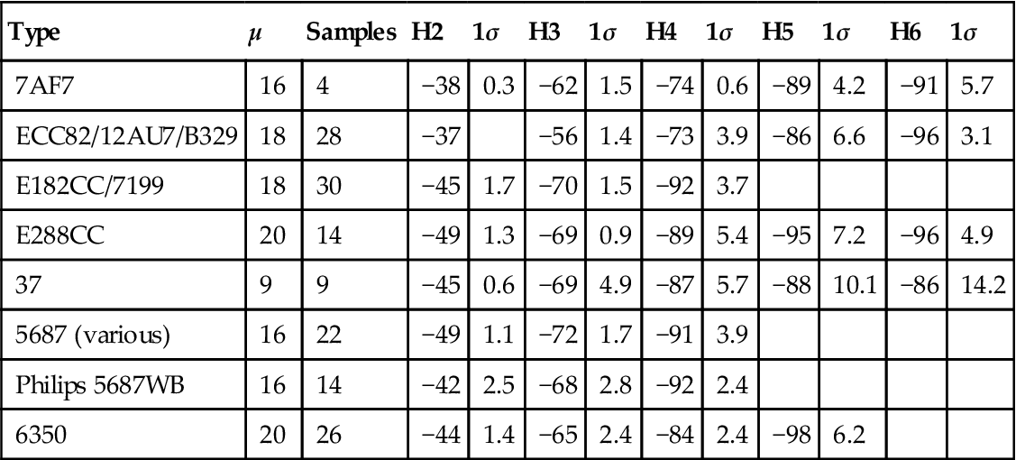
For each valve, μ was read from the manufacturer’s anode curves at the 8 mA operating point.
Table 3.13 allows quick comparison of these alternatives by normalising their distortion to the 6SN7GT/12SN7GT.
Table 3.13
Distortion (normalised to 6SN7GT/12SN7GT) of Electrical Alternatives to the *SN7/*N7 Family
| Type | Samples | H2 | H3 | H4 | |||
| dB | Ratio | dB | Ratio | dB | Ratio | ||
| 6SN7GT/12SN7GT | 44 | 0 | 1 | 0 | 1 | 0 | 1 |
| 7AF7 | 4 | +12 | 4 | +23 | 14 | +23 | 14 |
| ECC82/12AU7/B329 | 28 | +13 | 4.5 | +29 | 28 | +23 | 14 |
| E182CC/7199 | 30 | +5 | 1.78 | +15 | 5.6 | +4 | 1.58 |
| E288CC | 14 | +1 | 1.12 | +16 | 6.3 | +7 | 2.2 |
| 37 | 9 | +5 | 1.78 | +16 | 6.3 | +9 | 2.82 |
| 5687 (various) | 22 | +1 | 1.12 | +13 | 4.5 | +5 | 1.78 |
| Philips 5687WB | 14 | +8 | 2.5 | +17 | 7.1 | +4 | 1.58 |
| 6350 | 26 | +6 | 2 | +20 | 10 | +12 | 4 |
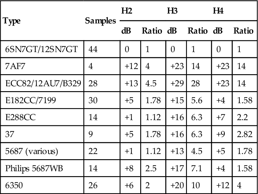
The results in Table 3.13 speak for themselves. All of the alternatives are inferior to the 6SN7GT/12SN7GT and produce significantly more H3.
The Loctal 7AF7 dual triode and B9A ECC82 dual triode are particularly ghastly. Perhaps significantly, these valves have an electrode structure that significantly reduced Cag compared to the *SN7/*N7 family (2.3 pF and 1.6 pF versus 4.0 pF). These tests suggest that the measures necessary to reduce Cag within the electrode structure might adversely affect distortion.
There was a significant difference between the Philips 5687WB and other manufacturers’ samples, so this type was isolated. Although H2 and H3 are significantly higher than competing manufacturers, H2 would mostly be nulled if used in a differential pair.
Weighted-Distortion Results
Towards the beginning of this chapter, distortion weighting was suggested as a useful technique, so Table 3.14 mathematically weights the measurements according to CCIR468-2 with a gain offset of −6 dB in order to make the H2 result comparable with an unweighted measurement. Because this particular test was limited to harmonics up to H6 (6.3 kHz is the corner frequency for CCIR468-2) and the distortion was dominated by H2 harmonic, the difference between CCIR468-2 less 6 dB and the Shorter recommendation was only ≈0.1 dB – well below measurement uncertainties, and validating Peter Skirrow’s CCIR468-2 single-measurement argument.
Table 3.14
Weighted Distortion Comparison of All the Valves Tested
| Type | Number of samples | Weighted distortion (dB) |
| Carbonised CV1988 | 12 | −58 |
| Carbonised 6SN7GT | 6 | −55 |
| Pinnacle 6J5GT | 138 | −52 |
| 7N7/14N7 | 144 | |
| GEC/Marconi B36 | 6 | −51 |
| 6SN7GT/12SN7GT | 44 | −50 |
| 12SX7GT | 12 | |
| 6J5GT (not Pinnacle) | 6 | |
| L63 | 5 | −49 |
| E288CC | 14 | |
| 5687 (not Philips) | 22 | |
| 7A4 | 3 | −48 |
| RCA 6J5 | 15 | |
| E182CC/7199 | 30 | −45 |
| 6350 | 26 | −44 |
| Philips 5687WB | 14 | −42 |
| 7AF7 | 4 | −38 |
| ECC82, 12AU7, B329 | 28 | −36 |
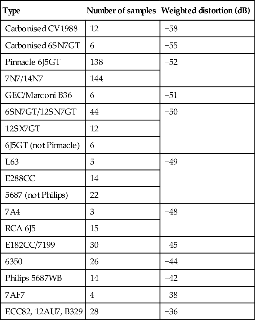
Overall Conclusions
A total of 529 valves was tested, and the results show that the reputation of the *SN7/*N7 family is well justified. Distortion for the dual triodes varied from sample to sample, with a few significant trends visible between manufacturers (probably because manufacturers were well known for buying in another manufacturer’s valves and branding them as their own in times of short supply). If individual measurement and selection for low distortion are not possible, then carbonised envelope valves from the *SN7/*N7 family are likely to produce the lowest distortion. If these are not available, then a 7N7, 14N7 or a Pinnacle 6J5GT is likely to be a good choice. Valves with electrode structures shrunk to fit B9A bases are significantly poorer.
Coupling from One Stage to the Next
The most common way of coupling one stage to the next is via a capacitor. A perfect capacitor does not generate distortion. Unfortunately, even a perfect capacitor can greatly exacerbate the distortion generated by valves or transistors.
Blocking
Blocking is an extremely unpleasant mechanism whereby an amplifier mutes for a short time after a momentary overload. In simple terms, blocking is caused by the capacitor that couples to a stage that is overloaded (see Figure 3.30).
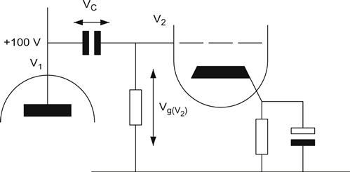
Capacitor coupling between two stages forms a high-pass filter. In order not to affect the audio, we deliberately design for a low f−3 dB frequency using:
Thus, setting f−3 dB=1 Hz means that τ=160 ms, but the true significance of τ in this context will take a little time to emerge.
Because of Kirchhoff’s voltage law, the following must be true at all times:
Example: ![]() , and the following grid is tied to ground via a grid-leak resistor, so
, and the following grid is tied to ground via a grid-leak resistor, so ![]() , causing VC=100 V.
, causing VC=100 V.
If we apply an impulse to V1 so that the anode swings 20 V positively, the grid of V2 attempts to rise to +20 V, but when it reaches +10 V, Vgk=0, and the grid conducts so heavily to the cathode that its voltage is clamped to +10 V. At this instant, the previous Kirchoff equation must still be true, so:
The capacitor was able to change its voltage almost instantaneously because it charged through the low impedance path of the overloaded grid. When the impulse passes, we can find the grid voltage of the second valve by rearranging the equation:
The grid is at −10 V, but the cathode is held at +10 V by the cathode bypass capacitor, so Vgk=−20 V, and the grid has reverted to a high impedance path. More importantly, the valve is now switched off and remains so until the grid recovers to 0 V. The only path for the capacitor to change its charge is through the grid-leak resistor, but as we saw earlier, this combination has a time constant of 160 ms. Worse, 5τ is required for the capacitor to change its charge to within 99% of its final charge, so the grid does not reach 0 V until 0.8 s after the momentary overload.
Recovery from overload is complicated by the fact that once the valve is switched off, there is no cathode current, so the cathode bypass capacitor begins to discharge through the cathode-bias resistor. Although this causes the valve to begin conducting earlier than would otherwise have been expected, it also has to recover from the change imposed by blocking. Thus, a momentary overload has had its effects extended to almost a second.
It might be thought that the severe overload posited to cause blocking is unlikely, but applying global feedback around a power amplifier containing a capacitor-coupled output stage almost guarantees blocking. Suppose that a transient causes clipping of the output stage. Feedback attempts to correct this distortion of the waveform by increasing substantially the drive to the output stage, and the requirements for blocking have been satisfied.
Blocking occurred because a coupling capacitor was allowed to change its charge significantly during an overload. If the capacitor could be eliminated, or moved so that it coupled to a stage that could not be overloaded, the problem would not arise. This technique will be explored in the non-blocking ‘Crystal Palace’ amplifier described in Chapter 6.
Alternatively, the time constant of the coupling capacitor could be reduced, reducing the duration of blocking. The price paid for this solution is low frequency attenuation in a zero global feedback amplifier or increased low frequency distortion in a feedback amplifier. However, if such an amplifier were part of a loudspeaker system having an active crossover (valve treble, semiconductor bass), degraded low frequency performance would be irrelevant. Stuart Yaniger’s ‘Red Light District’ amplifier available at the diyAudio website is a good example of this design philosophy.
Transformer Coupling
Transformers are expensive, but they are essential for connecting loudspeakers to valve amplifiers unless we are prepared to tolerate appallingly low efficiency. Inter-stage transformers offer some unique advantages:
• From the point of view of the primary, if the transformer is used as the anode load, the valve can achieve a much larger signal swing because the anode can theoretically swing to double the HT voltage if necessary. Alternatively, from a loadline point of view, the HT voltage has doubled, yet the signal swing has remained constant, typically halving the distortion compared to a resistive anode load.
• If the transformer steps down by a ratio of 2:1, the stage can produce the same swing as a resistively loaded stage, but with a quarter of the output resistance.
• A push–pull stage allows cancellation of even harmonic distortion.
• From the point of view of the secondary, a centre-tapped winding provides ideal phase-splitting.
• Larger power valves need low grid-leak resistances because of their grid current, so the very low RDC of the secondary is ideal.
Against these advantages we have to weigh the inescapable fact that inter-stage transformers suffer most from transformer imperfections because they operate at high impedances, and single-ended stages force the transformer to pass the (DC) anode current, requiring a gapped core, which reduces bandwidth.
Low Frequency Step Networks
One possibility sometimes seen in power amplifiers is to bypass the coupling capacitor with a resistor to form a step network. Low frequency step networks are best inserted just before a differential pair and may even ease their tail DC arrangements (see Figure 3.31).
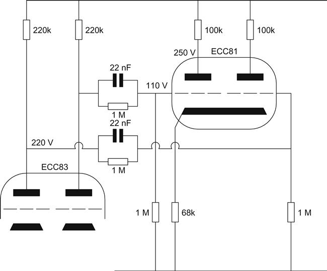
Note that because 110 V has been applied to the second valve’s grids, a simple resistor suffices for cathode bias, although performance would be improved if it were to be replaced by a CCS.
A step network is intermediate between DC and AC coupling. In the example, the step network is a 6 dB DC potential divider bypassed above 15 Hz by the 22 nF capacitors. The significance is that careful design can produce less low-frequency phase shift with a smaller capacitor than pure AC coupling and because reduced low frequency phase shift improves stability, more global feedback can be applied, reducing distortion. Further, blocking becomes less of a problem because the offending capacitor has a discharge resistor directly across it. Unless another low frequency time constant is dominant, step network time constants generally have to be determined by experiment because they are dependent on the (non-constant) primary inductance of the output transformer.
Level Shifting and DC Coupling
In the absence of PNP valves, DC coupled valve amplifiers rely fundamentally on the potential divider (see Figure 3.32).
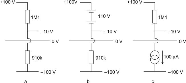
In Figure 3.32a, we have a simple resistive potential divider to the negative HT. We want to achieve −10 V at the output of the potential divider. Rather than use the potential divider equation, it is easier to set a current through the potential divider and apply Ohm’s law to find the required resistances. Our potential divider will steal current from the anode of the preceding valve, so we should minimise this current. If we set the potential divider current to 100 μA, the upper resistor must be:
Similarly, the lower resistor must be:
The nearest value of 910 kΩ is fine. Unfortunately, not only have we level shifted our signal by the required amount, we have also attenuated it. Thinking in AC terms:
Pure resistive level shifters inevitably attenuate the wanted AC, and this is the price that must be paid for simple DC coupling. A capacitor across the upper resistor would avoid the AC attenuation but create a step network which might not be desirable.
To maintain DC coupling without AC attenuation, we could replace the upper resistor with a battery, to make a Thévenin level shifter (see Figure 3.32b).
Because the battery is a perfect Thévenin source, it is a short circuit to AC, so this level shifter does not attenuate AC. Because 110 V batteries are inconveniently large, we would replace the battery with a Zener diode or neon reference valve. Sadly, both devices must pass a significant DC standing current (typically 5 mA), which makes them awkward to use. Worse, they both add noise.
Our final possibility is to replace the lower resistor with a constant current sink, to make a Norton level shifter (see Figure 3.32c).
There is no reason why we should not make a constant current sink out of bipolar transistors or a pentode. Provided that the sink has rout>>Rupper, the Norton level shifter does not attenuate AC. However, the noise problem remains. Pentodes and transistors are transconductance amplifiers, which means that they convert their input voltage into an output current. A current sink amplifies its DC reference voltage, and we propose to convert its output current back into a voltage using a high value resistor. In effect, we have constructed a high-gain amplifier that amplifies the noise voltage of the DC reference.
Although Thévenin and Norton level shifters are theoretically usable, their practical problem is noise, and almost all the design effort must focus on reducing this noise to acceptable levels. (Constant current sink tails in differential pairs do not add significant noise because the low impedance load rk severely reduces their gain, and their noise is applied common mode, so it is mostly rejected.)
Sadly, each of these techniques connects the signal to the negative HT, which may add hum and noise to the wanted signal.
A DC Coupled Class A Electromagnetic Headphone Amplifier
As with all amplifiers facing a difficult load, this circuit was designed working backwards from the output to the input. Be aware that the circuit is presented as a vehicle for investigating the problems of DC coupling – not as a detailed exemplar of headphone amplifier design.
A cathode follower is needed to provide a low output resistance. High-μ, high-gm valves are best suited as cathode followers because the high gm ensures low rout, and high μ allows plenty of feedback to reduce distortion, so the 6545P is ideal. The cathode is connected to the negative HT via a standard pentode constant current sink using an EL822.
We know that we want to apply DC feedback to stabilise the output of the amplifier at 0 V, and we need our completed amplifier to have a high input resistance so that it does not load volume controls. The ideal input stage is therefore a differential pair, and because we already have a negative HT, it seems churlish not to use another pentode constant current sink (see Figure 3.33).
Electromagnetic headphones are low impedance devices. Because portable equipment must operate from a 3 V battery (possibly only 1.5 V), headphones designed for portable use are typically 32 Ω, but better quality designs tend towards 200 Ω. Either way, they require considerable current, and are extremely onerous loads for valves. As we increase Ia, Pa rises, so we must reduce Pa by lowering Va as far as we dare without running into grid current. Setting Va=135 V keeps us just clear of grid current. Although it is claimed that Pa(max)=7.8 W, all the other 6C45_ specifications are somewhat optimistic, and the envelope is little larger than an ECC88, so it does not seem wise to operate at the full claimed power. If we set Ia=34 mA, then Pa=4.6 W.
We now need to consider the input differential pair. Because we only have 135 V of HT, we need a valve having good linearity at low voltages. The ECC86 would be ideal, but the ECC88 was available, and a little slithering of loadlines suggested that 27 kΩ load resistors would work well with an anode voltage of 68 V, resulting in a tail current of 5 mA at Vgk=2 V.
We are finally in a position to be able to investigate the more significant problems of DC coupling using a pure potential divider.
Each ECC88 anode is at 68 V. The grid of the 6545P cathode follower is at ≈−1.5 V (remember that we need the cathode to be at 0 V), so we must drop 69.5 V. If we were to set 100 μA of potential divider chain current, we would need an upper resistor of 695 kΩ, which is an awkward value. If we choose the nearest preferred value of 680 kΩ, our potential divider current becomes 69.5 V/680 kΩ=102.2 μA.
The lower resistor must drop from −1.5 V to −135 V=133.5 V, so 102.2 μA requires a 1.3 MΩ resistor, which is a preferred value. However, we need to consider another factor.
At the calculated anode voltage, the potential divider chain steals ≈100 μA current from the anode current of 2.5 mA. 2.5 mA is a low current for this valve, so sample variations between valves are greatly magnified, and the small stolen current is negligible by comparison. The theft/valve error pulls the output DC in the final circuit away from 0 V, so why not make the divider chain adjustable to compensate for valve variation? Using a 1.2 MΩ fixed resistor in series with a 250 kΩ resistor allows ±10% variation. You could apportion a larger value of variable resistance, but this would make the output DC adjustment more fiddly.
Even if the output DC is carefully adjusted to 0 V, it will drift. We need a means of forcing the output DC to 0 V, and the best way of doing this is to apply negative feedback. We connect our feedback network in parallel with the output of the amplifier, but because the output of the feedback potential divider is connected to the other grid of the differential pair, and the differential pair amplifies the difference between its inputs, it is in series with the input signal. The feedback is, therefore, parallel-derived, series-applied, so it reduces output resistance and increases input resistance. Reduced output resistance is significant because all contemporary electromagnetic transducers rely on rsource=0 to produce their designer’s intended transient response.
If we are to apply feedback, we must know how much gain is available. 27 kΩ is quite a low anode load resistance for an ECC88, and a loadline predicts a gain of 26.75. The input stage operates as a differential pair, but because only one output is used, we must immediately halve the gain to 13.375. We incur a loss of 0.657 in the level shifter, which reduces the gain to 8.78. Considering the 6545P, at Ia=34 mA, rk≈25 Ω, so a 32 Ω load incurs a further loss of 0.56, leaving a total gain of ≈5. Thus, even 100% global feedback could produce only (1+βA0)=5, or 14 dB, of improvement.
The circuit was tested with 100% negative feedback because this is the most critical condition for stability, yet delivered an exemplary square wave response at 10 kHz into a 200 Ω load (see Figure 3.34).
The circuit was tested into various load resistances.
Unsurprisingly, Table 3.15 shows that little valves don’t like 32 Ω loads and that this circuit can only deliver 8 mW at 0.5% THD+N into a 32 Ω load. The performance improves markedly into a 200 Ω load, whereupon the circuit delivers double the power at <0.1% THD+N and, more importantly, the spectrum of the distortion harmonics became acceptable: H2=−60 dB, H3=−82 dB, H4=−100 dB. Curiously, the author still does not own any electromagnetic headphones of plausible quality, so he was unable to test this amplifier subjectively.
Table 3.15
Headphone Amplifier Distortion Against Load Resistance
| Output in dBu for specified THD+N | |||
| 0.5% | 0.2% | 0.1% | |
| 100 kΩ | – | – | +20 |
| 200 Ω | +16.7 | +12.8 | +7.8 |
| 32 Ω | −3.7 | – | – |

Eagle-eyed readers having a 6C45_ datasheet will notice that this circuit far exceeds the maximum specified grid-leak resistance of 150 kΩ. Remember that the purpose of the grid-leak resistor is to hold the grid at its correct voltage in the face of grid current. If the resistor is too large, grid current raises the voltage on the grid, reducing Vgk, increasing Ia, causing more grid current, until the valve dies. In this circuit, Ia for the 6545P is set purely by the constant current sink, so considerations of thermal runaway caused by excessive grid-leak resistance are irrelevant.
If you need to set up a circuit of this type, it is easiest to break it into two parts before applying feedback. Build the output stage first, short-circuit the upper grid to ground, and adjust the CCS current programming resistor to set correct cathode follower current. Build the differential pair and associated CCS, and adjust the CCS current programming resistor to set required anode conditions. Connect the two stages, and fine-tune the level shifter for 0 V at the output. Finally, close the negative feedback loop.
Using a Norton Level Shifter
As mentioned previously, the Norton level shifter is a high-gain amplifier that amplifies the noise of its reference voltage. The noise problem can be tackled in various ways:
• Reduce the noise produced by the reference. Forward-biassed diodes produce less noise, so red LEDs may be useful. If a reverse biassed higher voltage diode must be used, use 5.6 V because this is a true Zener and quieter than higher voltages (which are avalanche).
• Noise isn’t a problem in itself; it becomes a problem when the signal voltage is sufficiently low that the signal-to-noise ratio is compromised. Solution: Don’t use Norton level shifters in pre-amplifiers.
• If the noise can be arranged to become common mode, then it can be rejected by a differential pair. This is the most powerful individual technique.
Don’t try to obtain all the noise advantage you need from one single technique – it is always better to use a combination of small advantages that sum to a large advantage.
Some years ago, the author picked up 40 N-channel and P-channel MOSFETs from a junk shop, and after passing them through his late lamented curve tracer, he found two reasonably complementary pairs. The hybrid idea promptly resurfaced, coupled with a wish to use some of the more obscure valves in stock. The author had previously been unable to find a use for the wonderfully high gm (55 mA/V) of the E55L, but realised that it might make a good cathode follower for driving the high-gate capacitance of MOSFETs. A little doodling resulted in a circuit requiring a Norton level shifter (see Figure 3.35).
The N-channel MOSFET needs +5 V on its gate to pass the required current of 1.7 A, whilst the P-channel MOSFET requires −6 V, so the Vbe multiplier between the gates allows these voltages to be applied and output stage current to be set. The E55L cathode follower has a power cascode constant current sink made from an MJE340 and a BC549 as its active load. The 7N7 differential pair has a cascode constant current sink tail that shares the reference voltage of the sink for the E55L. To balance the anode loads, the unused output of the 7N7 has an RC network to ground to simulate the input impedance of the E55L cathode follower. The ECC808 input differential pair is reasonably conventional except that it has constant current source anode loads to improve its linearity when operating from a positive HT of only +150 V.
Because the 7N7 differential pair is directly coupled to the E55L cathode follower, its grids must be at, or close to, the voltage of the negative HT, yet the anodes of the ECC808 are expected to be at +123 V. Thus, the problem is to DC couple the two stages with a minimum of noise.
Arbitrarily selecting 1 MΩ for the upper resistor of the level shifter suggests that the current passing through it will be ≈250 μA. We need to know this current because it is the design current for the constant current sink. If we choose a 6.2 V reference voltage, a 24 kΩ is required. If we treat the level shifter as a common-emitter amplifier, we can find its gain. Ic=250 μA, so gm=35Ic=35×0.25=8.75 mA/V. The gain of the amplifier is Av=gm·RL=8.75×1,000=8,750. However, the amplifier has considerable feedback because of the unbypassed 24 kΩ emitter resistor, so we can use the feedback equation:
Alternatively, now that we know that the gain before feedback is likely to be large, we can simply use the approximation:
The significance of this exercise is that a larger reference voltage reduces the gain of the amplifier because of the high value of Re that it enforces. Although a 1.6 V red LED would be perhaps 9 dB quieter than a 5.6 V Zener, it would enforce 14 dB more gain in the CCS, making it 5 dB noisier in this example.
If the level shifters share the (potentially noisy) DC reference, its noise is amplified identically, so it is presented to the differential pair as common mode noise, which it can reject. To ensure that the noise remains common mode, the emitter resistors and 1 MΩ must be matched, so 0.1% tolerance types are necessary. At high frequencies, the common-mode rejection of the differential pair deteriorates, but if we bypass the 1 MΩ resistors with capacitors to form a step network, the level shifter’s noise attenuation rises with frequency, tending to compensate for the differential pair’s falling CMRR.
Distortion and Negative Feedback
Negative feedback reduces distortion. All engineers agree on this, but shouting begins immediately afterwards regarding the character and subjective effect of the new distortion. Baxandall [10] investigated the problem in 1978 and originated the graph that has been reproduced elsewhere with little or no explanation (see Figure 3.36).
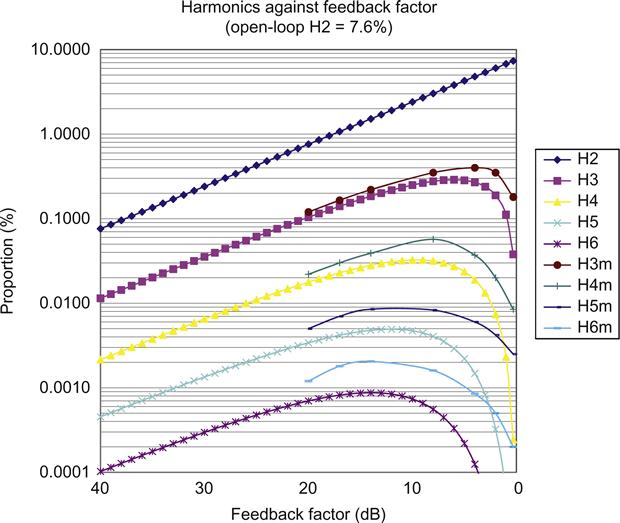
Baxandall’s original graph tested the hypothesis that if negative feedback was applied to a distorting amplifier, then the feedback signal would itself be distorted, generating harmonics of distortion harmonics, and that the amplitudes of these new harmonics could be predicted if the amplifier’s transfer characteristic was simple and known. The chosen amplifier was a resistively loaded 2N5458 common source JFET because theory indicated that a JFET’s distortion should be dominated by H2, and to ease the measurement problem, it was tested at a sufficiently high-signal amplitude to force 7.6% H2. As can be seen, the agreement between measurement and theory is good, but deteriorates as harmonic order increases because the fundamental assumption that the JFET produces only H2 becomes increasingly invalid at these distortion levels. It is vital to realise that the graph is the result of the need to set test conditions that would produce measurable data and whilst it vindicates the hypothesis, it does not represent real-world conditions and therefore almost all conclusions and extrapolations based on this raw graph are wrong.
Despite the previous damning statement, Baxandall’s hypothesis is useful because, as we saw earlier, triodes produce distortion dominated by H2 – and all that is necessary is to change the equation’s starting conditions (level of open-loop H2) to a more reasonable value (see Figure 3.37).
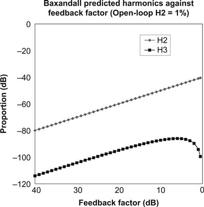
A triode amplifier might produce 1% distortion at the expected signal amplitude, dominated by H2, and the model shows that if 20 dB of negative feedback were to be applied, H2 would drop in amplitude by 20 dB (as we should expect), and feedback would produce H3 at an amplitude of −95 dB with respect to the fundamental. There are audio sources with noise/distortion floors better than −95 dB, but the most common digital source (CD) is 16 bit and this is its noise floor. In short, what Baxandall’s hypothesis really showed was that if the distortion spectrum after feedback is not to be questionable, open-loop distortion must be 1% or better.
Although it is difficult to design a power amplifier that produces <1% THD at full power dominated by H2 before applying feedback, designing small-signal stages to this standard is trivial. Thus, if we needed a line stage with a gain of 6 dB (perhaps to make up the 6 dB loss caused by inserting a balance control), we could load a triode from the *SN7/*N7 family with a constant current source to achieve an open-loop gain equal to μ (20), buffer it with a cathode follower (to avoid the feedback resistor loading the gain stage and increasing distortion), then apply 20 dB of feedback (see Figure 3.38).
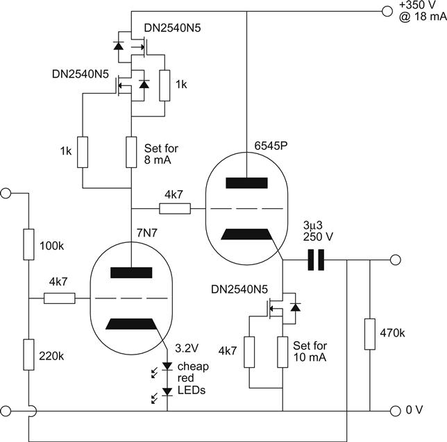
Referring to the measurements made earlier in this chapter, we would expect open-loop H2 at +28 dBu (19.5 VRMS) to be better than −50 dB, but at the more reasonable level of 2 VRMS, we could expect −70 dB (0.03%). Using 0.03% as the starting value in Baxandall’s equations predicts that H2 drops by 20 dB to −90 dB, and that the H3 produced by feedback will be entirely negligible at −156 dB. In practice, we know that the gain triode and cathode follower will produce small amounts of H3 and higher harmonics, but these will each be reduced by the feedback, and we can calculate their amplitudes (Table 3.16).
Table 3.16
Calculated Distortion Harmonics of CCS-Loaded *SN7/*N7 Before and After 20 dB of Negative Feedback
| H2 (dB) | H3 (dB) | H4 (dB) | |
| Before feedback | −70 | −105 | −110 |
| After 20-dB negative feedback | −90 | −125 | −130 |
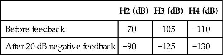
Summarising, negative feedback only degrades the distortion spectrum if distortion before feedback is >1%, otherwise it pushes all harmonics further into the noise floor.
Note, however, that there was a price to be paid for the low distortion; the grid circuit now has a 100 kΩ series resistor that generates noise and therefore degrades the signal-to-noise ratio of the compound stage.
Carbon Resistors and Distortion
Carbon has much higher resistivity than manganin (resistance wire), so a shorter path gives the same resistance. Since resistors are commonly constructed as a helix, higher resistivity means fewer turns and reduced inductance, so we use carbon resistors for valve and FET grid/gate stoppers.
However, not only are carbon resistors noisy, but they also produce distortion. Bailey (better known for ‘transmission line’ loudspeakers and long-haired wool) warned in an article on designing an audio generator with less than 0.02% distortion [11] that ‘It is important that only wire-wound resistors are used in the filter, as carbon types are non-linear and can produce distortions of up to 0.5%. This non-linearity is often overlooked, but where low levels of distortion are being dealt with, the results may be very serious.’
A quick test of a 100 kΩ carbon resistor in a potential divider revealed resistor distortion at −81-dB H2 and −71-dB H4. Whilst not as bad as Bailey’s example, the fact that a single resistor can produce measurable distortion is distinctly alarming.
Nevertheless, carbon is still a valid choice for grid/gate stoppers because the distortion is caused by the resistor’s non-linear voltage to current relationship, and if there is no grid/gate current through the resistor, there can be no series voltage developed across it and there can be no distortion.
Noise
In this section, I will define noise to be strictly uncorrelated random events possibly due to the granularity of a current that is the sum of individual electrons over time. More simply, we will include thermal noise and its relatives, but exclude man-made interference. To maximise dynamic range, we must minimise noise.
Noise from Resistances
We saw in Chapter 1 that all resistances produce a noise voltage:
k=Boltzmann’s constant ≈1.381×10⁻²³ J/K
T=absolute temperature of the conductor šC+273.16
This leads directly to the well-known requirement that low-noise amplifiers should minimise the value of their resistances to minimise noise.
Noise from Resistive Volume Controls
At some point in the amplifying chain, we need a means of controlling volume, with variable attenuation from 0 dB perhaps up to 60 dB. All resistive volume controls can be reduced to a potential divider, so at the same time that the control is attenuating the signal, it is also generating noise. If we assume that the source resistance feeding the volume control is negligible, as far as noise is concerned, the two resistors of the potential divider are in parallel, so we can find that parallel resistance and calculate its noise voltage (over a 20 kHz bandwidth). Because the volume control attenuates, the noise generated at the output of the volume control must be compared with that attenuated signal. If we assume a peak input level of 2 VRMS, we can determine the signal to noise ratio of a 100 kΩ volume control at various attenuations (see Figure 3.39).
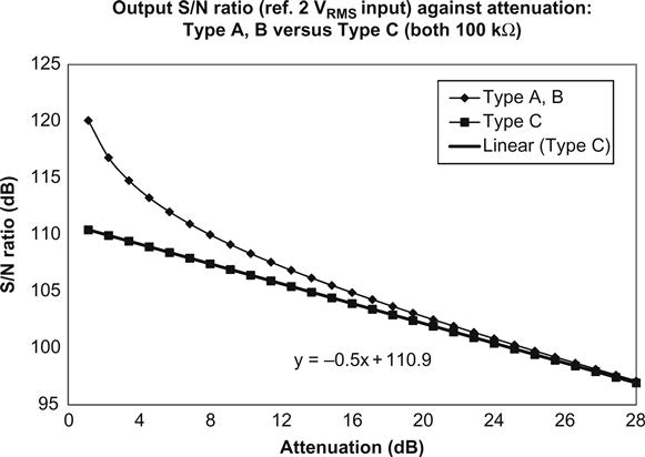
We will investigate detailed design of volume controls in Chapter 7, but suffice to say that a Type C attenuator has a fixed value series resistor with variable shunt, whereas the Types A and B can vary both series and shunt arms. Note that for the specified values of input voltage and resistance, as attenuation increases, all three types tend towards a signal to noise ratio of 111 dB minus half the value of attenuation (in dB). More importantly, if we reduce the input signal from 2 VRMS to 1 VRMS (−6 dB), we immediately reduce the signal to noise ratio by the same amount. Now imagine that we have an amplifier with an input sensitivity of 400 mVRMS and we connect it to a digital source (2 VRMS) via a volume control. At maximum volume (before the amplifier overloads), we must have 14 dB of attenuation, so we have limited our maximum signal to noise ratio to 97 dB purely because of noise in the volume control.
If we require the same signal to noise ratios at 400 mVRMS that we had at 2 VRMS, we must reduce our volume control resistance from 100 kΩ to 5 kΩ, and this is why semiconductor electronics typically has this value of volume control. Alternatively, we could state that since valve electronics generally needs a 100 kΩ volume control, it must be at a point of 2 VRMS sensitivity. (As an example of noisy design, the Leak Stereo 20 power amplifier and Point One Stereo pre-amplifier combination placed a 100 kΩ volume control at a point of 125 mVRMS sensitivity, resulting in a maximum signal to noise ratio purely due to the volume control of 87 dB.)
Noise from Amplifying Devices
There are two distinct noise sources within a triode and, like a transistor, their relative amplitude determines the optimum source resistance. Internal shot noise due to the granularity of anode current can be considered to be a voltage source at the grid (usually expressed as the value of resistance that would produce that noise voltage). Remembering that the noise produced by a resistor is:
And that the equivalent noise resistance of a triode is approximately:
Substituting we get:
Thus, voltage noise referred to the grid is proportional to the inverse square root of gm and this is the reason why quiet RIAA stages for moving coil cartridges require high-gm valves such as E810F, D3a and EC8010.
The granularity of (unwanted) control grid current forms a current source, and a valve’s optimum source resistance is therefore:
Although this equation predicts the optimum source resistance for a given input stage, it doesn’t guarantee minimum noise – after all, we could quadruple both voltage and current noise and obtain the same optimum source resistance with a noisier amplifier. However, what the equation does tell us is that high source resistances require low grid current noise. We can see this intuitively by observing that any grid noise current must pass through the source resistance and develop a voltage across it, so the smaller the current, the smaller the voltage. Note that although reactances cannot produce noise, Ohm’s law guarantees that driving a noise current through the inductance of a moving magnet cartridge converts grid current noise into a noise voltage. Nevertheless, in a noise source context, even moving magnet cartridges are not high impedance and the grid current noise of a competently manufactured valve ought to be insignificant even with a high inductance moving-magnet cartridge.
However, capacitive transducers are unquestionably high impedance sources, and for audio that means condenser microphones. The typical large (20 mm) capsule microphone popular for lead vocals has a source capacitance of ≈30 pF and, for such a source, it is not grid voltage noise that must be minimised but grid current noise.
Grid Current Noise and the Poisson Distribution
Before investigating how to minimise grid current noise, we must make a very brief foray into statistics. Valve control grid current is so low that we are concerned with the exact number of electrons that leave or enter the grid circuit. If we were to consider 1 μs slices of time, and each 1 μs slice contained exactly the same number of electrons, then there would be no audible noise current because it is the variation (AC component) that we hear, not the DC component.
The valve manufacturers will always have designed to minimise grid current noise, and therefore the probability of a given physical process resulting in an electron that contributes to grid current is low, but thermal agitation ensures that there is a large number of tests, so their statistical result has a Poisson distribution. The significance is that a Poisson distribution is completely described by its mean value, and:
This equation is the Ohm’s law of statistics and that square root relationship is ubiquitous in noise calculations.
For audio purposes, the mean is the DC component of a current (or voltage) and the standard deviation is the AC (noise) component. Thus, if we want to minimise grid current noise (standard deviation), we must minimise the (unwanted) grid current. Note that this argument does not apply to the valve’s internal shot noise because we need the anode current in order to modulate it, so it is the ratio between the standard deviation and the mean that must be minimised.
Electrometers and Grid Current
Whereas a DVM might measure currents down to fractions of a microampere, an electrometer is an instrument designed specifically to measure very small currents, typically ranging between 1 fA (10−15 A) and 1 nA (10−9 A). When investigating electrometer input valves, Dagpunar [12] showed that grid current could be split into broad categories, firstly determined by whether electrons were arriving (positive grid current) or leaving (negative grid current). Given that each positive ion arriving at the grid surface requires one or more electrons to leave the grid to discharge it, arriving positive ions contribute to negative grid current.
Positive grid current is due to:
I1 Electrons leaving the cathode but intercepted by the grid.
Negative grid current is due to:
I2 Photoelectric and thermionic electron emission leaving the grid. Positive ions arriving from the heated cathode (atoms of cathode-emissive material). These sources produce a fixed number of electrons/ions within the valve’s grid/cathode region, so Vgk simply determines how many are collected, leading to a saturation value irrespective of Vgk.
I3 Positive gas ions caused by the direct impact of accelerated electrons during their flight to the anode. Positive gas ions caused by the Bremmstrahlung (braking radiation) and X-rays produced by the anode due to arriving electrons being abruptly decelerated. Positive ions of anode material dislodged or emitted from the anode heated by electron bombardment.
I4 Secondary electrons emitted from the grid due to the impact of positive ions.
I5 Surface leakage over glass or insulation inside and outside the valve. This is assumed to be a resistive component, directly proportional to Vgk. Brimar [13] noted that the most common cause of noise variation between valves of the same type was grid current noise caused by surface leakage currents across mica spacers and stray fibres or lint between electrodes. In a similar vein, the external surfaces of electrometer valves must not be touched with bare fingers as traces of sweat will cause surface leakage currents.
When represented graphically these idealised categories sum to produce the familiar grid current curve with its crossover point typically at Vg≈−1 V (see Figure 3.40).
Each individual physical noise process was earlier assumed to have a Poisson distribution, implying that the standard deviation (noise) was equal to the square root of the mean. But we have seen that grid current is due to a number of sources, so total grid noise current must be the power summation of individual noise sources, and this is why grid current noise does not fall to zero at Ig=0, but has a very broad minimum at the inflection of Ig (Vgk=−4 V in this model). Note that any change in individual noise sources (and particularly leakage) will completely change the noise current curve.
Photoelectric emission from the grid is easily minimised by operating the valve in darkness, but it is currently fashionable to mount a bright LED in the valve base that shines directly into the valve’s internal structure. Whilst this is clearly the worst possible photoelectric scenario, any application that is sufficiently insensitive to hum to allow the valve to be on display is also insensitive to the increased grid current noise due to LED illumination. However, remember that LEDs are easily capable of tracking a 100 Hz/120 Hz hum waveform and its harmonics, so it would be unfortunate to prove that an illuminated valve was sensitive to optical hum – if you must have a light show, use clean DC for the LED.
Prior to the production of valves designed specifically for electrometers, Gillespie [14] investigated the possibility of using the Mullard EF37 in an electrometer, and found that there were three practical ways of reducing the grid current of a given valve (ranked in order of decreasing effectiveness and categorised according to Dagpunar):
I3 Reducing anode voltage reduces the energy involved in a collision between an accelerated electron and a gas molecule. Gillespie stated that gas/ion current varies with the square of accelerating voltage, so electrometer valves typically operate with an accelerating voltage of only 10 V (whether provided by the anode or screen grid).
I3 Biassing the grid further negative reduces anode current and therefore the number of collisions between electrons and gas molecules, thereby reducing gas/ion current.
I2 Reducing heater dissipation reduces grid electron emission and cathode ion emission. (Dedicated electrometer valves avoid indirectly heated cathodes because the unavoidable temperature drop across the heater/cathode insulation requires the heater needs to be hotter, increasing photoelectric emission.)
Gillespie found that because grid electron emission and cathode ion emission are second-order effects, reducing heater dissipation was only worthwhile if all other sources of grid current had been minimised and the valves had been selected for low grid current. Only one valve in six passed Gillespie’s low grid current selection process, so when Mullard adopted it, such EF37s were released as type ME1400.
Despite the previous caveats, the reduced heater dissipation technique has erroneously entered audio folklore as a general solution for low noise, yet only a condenser microphone head amplifier using a valve previously selected for low grid current would be likely to achieve a noise reduction from judicious reduction of heater dissipation. Unfortunately, reducing heater dissipation drastically reduces gm, increasing grid voltage noise, so it seems unlikely that an improvement of more than 1–2 dB could be gained.
We can summarise grid current noise by stating that for a competently manufactured valve:
• Grid current noise is only significant with high source impedances and for audio, which means condenser microphones.
• Grid current (and its noise) is highly sample dependent because it is usually dominated by surface leakage currents, but a quiet valve is likely to have a very broad minimum well away from the crossover voltage.
The crucial significance of this investigation into grid current noise and making the distinction between a valve’s internal shot noise and its grid current noise is that whereas the magnitude of the internal shot noise can be predicted reasonably accurately by fundamental physics, the magnitude of grid current noise is wholly dependent on the vicissitudes of production engineering.
It must be remembered that valves were/are assembled by hand, requiring considerable manual dexterity and attention to detail. Experience shows that manufacturing processes dependent on skilled manual labour require not only a motivated workforce adroitly directed by a good engineer/manager, but also, more importantly, a great deal of practise to determine the exact production technique necessary to meet the required standard, and even in the golden age, valves needed to be selected when low grid current was required. The valve market is far smaller now than in its heyday, so economies of scale can no longer be applied, making the production engineering problem far greater. In short, making valves is high technology dependent on mass production, and it is unrealistic to expect small runs of contemporary valves to achieve the low grid current noise or consistency of selected golden age valves.
Noise in DC references
We occasionally need a DC reference voltage. The most obvious example is the reference in a regulated power supply, but we might also need a reference to enforce operating conditions in an amplifier. We will investigate the DC reference in a regulated supply because it produces some initially counter-intuitive (but very useful) results.
The typical series regulator is nothing more than a non-inverting power amplifier amplifying the DC reference. As an example, if we had a 317 IC regulator with a reference voltage of 1.25 V and needed an output voltage of 15 V, we would choose external resistor values that caused the amplifier to have a gain of 12. But this means we have also amplified the noise voltage of the DC reference by a factor of 12, and this is why the 317 datasheet specifies the output noise voltage as a percentage of output voltage.
If we need a high voltage, it seems sensible to start with a high-voltage DC reference and amplify it only a little rather than start with a low voltage and suffer higher noise amplification. The key factor is the noise produced by the reference. Sadly, not all the gas DC reference datasheets specified their noise voltage, and information on how that measurement was made was sparse. Clearly, it was time for the author to make some measurements.
How the Author’s DC Reference Noise Measurements Were Made
The references were all operated at a current of 5 mA set by a cascode DN2540N5 JFET constant current source powered from a filtered DC supply. Noise was measured by an MJS401D audio test set coupled by an input transformer to improve rejection of mains hum and a capacitor coupled to protect that input transformer (see Figure 3.41).
The test set was set to RMS rectifier in order to make the results comparable with datasheets. Unless specified otherwise, bandwidth was limited by the MJS401D’s maximally flat 36 dB/octave 22 kHz low-pass and 18 dB/octave 22 Hz high-pass filters. This bandwidth is wider than the 10 Hz to 10 kHz bandwidth commonly used by device manufacturers, but remembering that noise is proportional to the square root of measurement bandwidth:
which amounts to −3.4 dB, and enables comparison of measurements. As an example, the author measured 138 μVRMS of noise over a 22 kHz bandwidth from a batch of 85A2s, which corresponds to 93 μVRMS over a 10 kHz bandwidth, but the Mullard 85A2 datasheet claimed ‘of the order of 60 μVRMS’, which is 4 dB quieter. (Mullard didn’t explicitly state ‘RMS’, but stating that the noise was equivalent to a 22 MΩ resistor implies RMS.) There are four possibilities for this 4 dB discrepancy:
• The devices have deteriorated over the decades and become noisier.
• The devices needed to be operated for 3 min to achieve their lowest noise.
• The Mullard measurement used a different rectifier (perhaps average reading but calibrated RMS on sine wave) plus smoothing.
• Mullard determined 85A2 noise by comparison. A noise meter could have been switched between the 85A2 and a selection of resistors, and when the two readings were equal, the noise deemed to be that of a 22 MΩ resistor.
The first possibility seems unlikely, and although the second is true for DC stability, no noise change was observable over 2 h. The third possibility could account for 1 dB (switching from RMS to average reading gave a 1 dB reduction on the author’s MJS401D). However, the fact that the noise is stated to be equivalent to that of an E6 standard value resistor suggests that this was the method used, and it could be that the noise measurement on the resistor produced higher noise than should be expected from the square root of 4kTBR. One distinct possibility is that any grid current noise from the noise meter’s input amplifier would develop a significantly higher noise voltage across a 22 MΩ resistor than across the typical 300 Ω slope resistance of a gas reference, leading to a falsely small value of resistor being needed for equal noise, and thus a perceived lower gas reference noise.
There is always a danger when measuring small signals that the measurement is actually of interference such as mains hum or ADC sampling noise from DVMs. As a check, a Tektronix 2213 analogue oscilloscope and a TDS3032 digital oscilloscope were connected to the monitoring output of the audio test set. If the audio test set was measuring pure noise, then setting the digital oscilloscope to average over 512 samples should average the noise nearly to zero and no coherent waveform should remain. Mains hum was the most likely source of interference, so the digital oscilloscope was triggered from AC line to ensure that averaging revealed mains hum if present.
Similarly, there is a danger that the test set’s own noise could be confused with external noise. With no input, MJS401D self-noise measured with 22 Hz to 22 kHz filter and RMS rectifier was −116 dBu.
Gas Reference Noise Measurements
Sadly, the author doesn’t have very many gas references, so the statistical validity of the following measurements is somewhat questionable, although sample variation was very low at <1 dB for all devices.
Table 3.17 shows that there is very little difference in the voltage-referred noise between devices, although a 108 V reference appears to be a quieter choice than the ubiquitous 85 V 85A2.
Table 3.17
Comparison of Noise for Various Gas Reference Valves
| Number of samples | Average noise (dBu) | Reference voltage | Voltage-referred noise (μV/V) | Voltage-referred noise (dB) | |
| 75C1 | 3 | −74.5 | 75 | 1.46 | −0.9 |
| 85A2 | 9 | −75.0 | 85 | 1.62 | 0 |
| 85A1 | 1 | −74.0 | 85 | 1.82 | +1 |
| QS1215 | 1 | −75.5 | 90 | 1.45 | −1 |
| QS95/10 | 2 | −72.7 | 95 | 1.67 | +1.3 |
| VR105/30 | 4 | −74.5 | 105 | 1.39 | −1.3 |
| CV286 | 4 | −74.3 | 108 | 1.38 | −1.4 |
| 0B2 | 6 | −74.3 | 108 | 1.38 | −1.4 |
| QS150/15 | 10 | −69.2 | 150 | 1.78 | +0.8 |
| 0A2 | 5 | −69.8 | 150 | 1.67 | +0.3 |
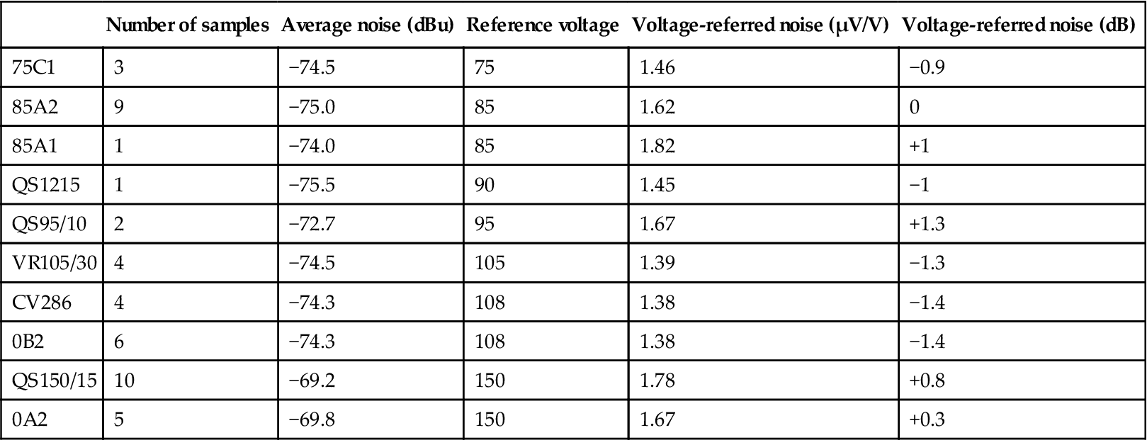
Voltage-referred noise is the measured noise voltage divided by the reference voltage and is thus an absolute indicator of the noise the device would contribute when used in a typical regulator. Voltage-referred noise in dB is referenced to the 85A2.
Variation of Gas Reference Noise with Operating Current
We have previously seen that noise is due to the granularity of current, so we should expect the noise of a reference to be proportional to the inverse square root of operating current. A Mullard 0B2 was tested over a 4–26 mA range (see Figure 3.42).
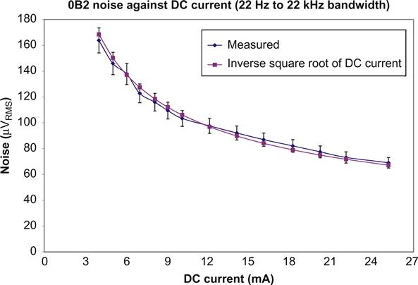
The uncertainty of the noise measurements was estimated to be ±0.5 dB, so this uncertainty has been added to each measurement as an error bar. An inverse square root relationship passes comfortably through the error bars, and although a flatter coefficient (I−0.475) gives a better fit, inverse square root is quite good enough when choosing operating current.
To sum up, the 108 V references seem the quietest, and noise is inversely proportional to the square root of operating current. Having investigated gas references, the author realised that (for completeness) some semiconductor reference measurements ought to be made.
Semiconductor Reference Noise Measurements and Statistical Summation
Since the series of gas reference tests had been referred to the 85 V 85A2, it not only seemed sensible to compare semiconductors at a similar voltage, but it was expected that the noise of such a high voltage reference would be easier to measure. Thus, 16 BZX55 Zeners having a nominal voltage of 5.6 V were connected in series to produce an 84 V composite Zener. Using the same test set-up as before, this composite Zener produced noise at −101 dBu, which is 29 dB quieter than the 85A2.
A 29 dB noise improvement is so enormous that it immediately questions the measurement technique, so the 85A2s were immediately checked and their noise confirmed. 5.6 V is a quiet voltage still within true Zener action, but as Zaphod Beeblebrox [15] complained, ‘leaves us a very large improbability gap still to be filled’. The improbability gap is that the noise of each individual Zener is uncorrelated with the others, so noise powers must be summed and the noise of the composite Zener is not 16 times the noise of each individual Zener, but only four times. This technique is the dual of reducing current noise by connecting n devices in parallel to reduce their noise by √n.
If the √n hypothesis is true, connecting an even larger number of Zeners in series should produce a predictable noise advantage, and this was tested. Thirty-five 5.6 V Zeners were connected in series to form a composite 195 V Zener. If the √n hypothesis is true, the noise advantage produced by this new reference compared to the old should be:
Had the √n hypothesis been untrue and the noise sources correlated, we would expect increasing the reference voltage from 84 V to 195 V to increase noise by 7.3 dB (195/84), but the hypothesised 3.4 dB statistical noise advantage should reduce this to 3.9 dB. With both composite Zeners measured at 10 mA, the 84 V composite Zener produced noise at −103 dBu, whereas the 195 V composite Zener produced noise 4 dB higher at −99 dBu, confirming the √n hypothesis.
Variation of Zener Reference Noise with Operating Current
We saw earlier that the 0B2 gas reference produced noise inversely proportional to the square root of its operating current, and the same statistics should apply to the composite Zener. After careful optimisation of the test set-up, uncertainties at these measurement levels were reduced to an estimated 0.7 dB (unavoidably 0.2 dB higher than obtained in the gas reference tests) (see Figure 3.43).
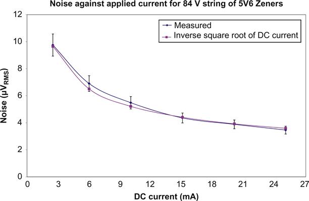
As can be seen, an inverse square root curve once again passes through the error bars, confirming the hypothesis. But this result is more significant than before because a 5.6 V BZX55 (500 mW) has a current rating of 89 mA, so we could safely pass a much higher current than we could through a gas reference. 25 mA would not be an unreasonable current, reducing the 84 V composite Zener noise to −107 dBu, or 3.5 μVRMS measured over a 22 Hz to 22 kHz bandwidth.
Noise of the Composite Zener Compared to a 317
The 317 IC regulator has been mentioned in passing, and Linear Technology’s 317 datasheet [16] states that a 317 produces noise (10-Hz to 10 kHz bandwidth, RMS rectifier) equal to 0.001% of output voltage, so if we needed a 195 V supply we would expect it to produce 1.95 mVRMS of noise. By comparison, the 195 V composite Zener passing 10 mA produced 8.7 μV of noise over a 22 Hz to 22 kHz bandwidth. Adjusting for bandwidth, this makes the 195 V composite Zener 50 dB quieter than the 317. Admittedly, the usual speed-up capacitor added to the 317 reduces its noise gain at high frequencies, but it must have full gain at DC, and to avoid destroying transient response, the speed-up capacitor only becomes effective >100 Hz, implying ≈100 Hz noise bandwidth and therefore a 20 dB improvement compared to the 10 kHz noise bandwidth, reducing the noise advantage of the composite Zener to 30 dB.
As an aside during the semiconductor DC reference tests, the author tried an 84 V composite device made up of seven BZX55 12 V avalanche diodes, and at 10 mA it produced noise at −75 dBu (comparable with the gas DC references but 28 dB worse than the 5.6 V version). To be fair, the 12 V devices suffered a 3.6 dB statistical disadvantage compared to the 5.6 V, but it does seem that the 12–15 V region is a particularly noisy avalanche voltage. A single ZPY56 56 V device was tried at 6 mA, and this produced noise at −82 dBu, which is significantly better than the gas DC references, but not nearly as good as the composite devices using 5.6 V Zeners.
Red LED Noise
Finally, the author measured a string of HLMP6000 red LEDs. These LEDs are reputed to be very quiet, so 105 were soldered together to form a 167 V reference. Noise did not vary smoothly with current (although it was repeatable), perhaps suggesting a questionable soldered joint. Nevertheless, the results normalised to 84 V suggested that the LEDs were better than 6 dB quieter than the composite Zener using 5.6 V devices. However, whilst hand-soldering 35 wire-ended Zeners in series on a tag strip is perfectly practical (if a little tedious), hand-soldering 105 LEDs isn’t, restricting the use of LEDs to low-voltage references, although a surface mount ‘pick-and-place’ machine followed by wave soldering would undoubtedly have no trouble reliably making a high-voltage low-noise (but rather expensive) reference.