
For a typical internal temperature of 40°C (313 K), with a bandwidth of 20 kHz, this is more conveniently expressed as:
Using this equation, we find that a perfect 100 kΩ resistor generates 5.9 μV of thermal noise. In this instance, the resistor’s thermal noise has been greatly exceeded by its excess noise. To find the total noise of the resistor, we must add the individual noise powers, which, if we remember that P=V2/R, means that
This gives a total noise for the resistor of 21 μV, and was rather tedious, but it demonstrates two points:
• For wirewound resistors we need only calculate the thermal noise. (No excess noise.)
• For metal film resistors we need only calculate the excess noise. (This simplification works because in practical circuits, as the DC voltage across the anode load resistor falls, so does its required value, and therefore its thermal noise.)
Now that we have simplified the noise sources in the resistor, we can see how they will be shunted by the ra of the valve, and redraw the circuit (see Figure 7.34).
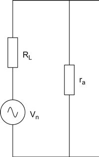
It is now easy to see that the circuit is a potential divider and that the actual contribution of resistor noise to the circuit is equal to the open circuit resistor noise multiplied by the attenuation of the potential divider. In our example, this reduces the noise of the resistor from 21 μV to 1.26 μV. It should be noted that if Rk is left unbypassed, ra rises dramatically and it is no longer able to shunt resistor noise.
If we divide the noise voltage by the gain of the stage Av=29, we can find the input referred noise, which is 43 nV. The significance of this is that it enables us to sum this noise with any noise sources at the grid, such as the grid-leak resistor. In practice, if we calculate the thermal noise generated by Rg and its attenuation by the cartridge, we generally find that it is insignificant compared to the valve noise. In any event, we do not have a choice about Rg since it is set by the cartridge.
Valve Noise
We should now consider the shot noise within the valve itself. Valves produce shot noise because Ia is made up of individual electrons that shower the anode, and also because electrons leave the cathode with random velocities to join the space charge, so this implies that cathode chemistry could affect noise.
For triodes:
This says that the white shot noise generated within the valve is equivalent to the thermal (white) noise generated by a perfect resistor req at the input of the valve. For our example triode, gm≈5.3 mA/V, so the equivalent noise resistance would be 470 Ω.
Using ![]() , the input voltage noise produced by the valve is therefore ≈400 nV and swamps the 43 nV (input referred) noise produced by the anode load resistor (as it should, in a good design), and we need not sum the noise powers of the valve and the resistor.
, the input voltage noise produced by the valve is therefore ≈400 nV and swamps the 43 nV (input referred) noise produced by the anode load resistor (as it should, in a good design), and we need not sum the noise powers of the valve and the resistor.
For pentodes [7]:
Applying this equation to the low-noise EF86 pentode operating at Ia=1.25 mA, ![]() predicts a noise resistance of 3.9 kΩ and a noise voltage (20 kHz bandwidth) of 1.2 μV. However, Mullard measured 2 μV for a noise bandwidth of 25 Hz to 10 kHz under the same DC conditions, which corresponds to 2.8 μV for a 20 kHz bandwidth, making it 7.4 dB noisier than the prediction.
predicts a noise resistance of 3.9 kΩ and a noise voltage (20 kHz bandwidth) of 1.2 μV. However, Mullard measured 2 μV for a noise bandwidth of 25 Hz to 10 kHz under the same DC conditions, which corresponds to 2.8 μV for a 20 kHz bandwidth, making it 7.4 dB noisier than the prediction.
For JFETs [8]:
JFETs are common in hybrid valve/transistor circuits, and as the previous equation shows, they are quiet. Their equivalent noise resistance is not only substantially lower than for a triode (effectively 5.5 dB quieter for a given gm), but they also tend to have higher gm for a given anode or drain current. The quietest JFETs currently available are the Linear Systems LSK170 (derived from the Toshiba 2SK170) and Philips BF862 – both produce ≈1 nV/√Hz noise, making them entirely suitable for moving magnet cartridges, but not quite quiet enough for moving coils.
1/f Noise
Unfortunately, the preceding noise equations do not tell the whole story at audio frequencies because they do not account for 1/f noise, but they do indicate that pentodes are much noisier than triodes and that gm should be maximised. Provided that the cathode has been made properly, 1/f noise is due to grid current noise and, as we saw in Chapter 3, this is largely down to manufacturing cleanliness, making it sample dependent. However, the clean room conditions needed to manufacture semiconductors mean that manufacturers of low-noise Bipolar Junction Transistors (BJTs) are able to provide graphs that show how noise varies with frequency. The lower the 1/f corner frequency, the better it will be.
Connecting Devices in Parallel to Reduce noise
High-gm valves are so expensive that we might choose to increase gm by connecting a number of devices in parallel, since the noise falls by a factor of √n. The MAT02/LM394 supermatch transistor is an extreme example of this technique, as it contains a pair of composite transistors each made of 100 individual devices to give a 20 dB improvement. Paralleling 100 E88CCs is impractical, but a worthwhile, if somewhat modest, improvement of 4.5 dB can be gained by using three devices in parallel. Note that the input capacitance trebles, outlawing input transformers, moving magnet cartridges, and even some moving coil cartridges. (The high output moving coil Sumiko ‘Blue Point Special’ specifies maximum load capacitance as 200 pF.)
Unfortunately, the previous examples demonstrate an important point. Although we may improve noise by a better choice of input valve, or valves, we pay dearly for quite small improvements, since obtaining a high gm is expensive and invariably current hungry. To minimise noise, it is always better to present the input stage with a healthy signal, rather than hope to amplify a weak one cleanly.
Valve Noise Summary
Despite all the previous caveats, qualifications and provisos, we can make some useful generalisations that will avoid unnecessary calculations when designing for low noise:
• Pentodes are significantly noisier than triodes, and JFETs can be even quieter.
• Valve sample variation can be large. (1/f noise is largely determined by the cleanliness of the room in which the valve was assembled, so although a given manufacturer tends to be consistent, there can be differences between manufacturers – or more accurately, their assembly rooms.)
• To render the noise of RL insignificant, there must be no feedback at the cathode, since this reduces the shunting effect of ra. This is also true for a μ-follower, even though omitting Ck has no discernible effect on gain. The cascode has ra≈∞, so the noise from RL must be considered.
• Maximise gm for low noise, either with a single excellent device, or with a number of lesser devices in parallel.
• Maximised gm invariably raises the input capacitance of the input stage and may preclude using a moving-coil step-up transformer.
• Excess noise dominates in film resistors passing DC. Wirewound and bulk foil resistors do not produce excess noise.
• A very large (typically 100 times normal) coupling capacitor allows ra to shunt the noise generated by the grid-leak resistor of the following stage, but DC coupling would be even better.
Together, these noise and input capacitance considerations all but eliminate the ECC83, 6SL7GT, and other high-μ, low-gm valves from the input stage of an RIAA stage.
Noise Advantage due to RIAA Equalisation
Numerical integration of RIAA equalisation (3,180 μs, 318 μs and 75 μs) from 20 Hz to 20 kHz using thirtieth octave bands gives a noise equivalent bandwidth of 94 Hz, which reduces noise by 22.3 dB, but because the equalisation imposes a gain of 19.9 dB referred to 1 kHz, the final advantage due to equalisation referred to the 1 kHz sensitivity is a meagre 3.4 dB (unchanged if the 3.18 μs time constant is implemented). The significance of this 3.4 dB figure is that if the input referred noise and input sensitivity is known, a full post-RIAA signal-to-noise ratio may be predicted.
Stray Capacitances
We now know that our input valve is likely to be a high-gm valve such as an E88CC, or better, and if we assume a required input sensitivity of 2.5 mVRMS at 1 kHz 5 cm/s, this is likely to result in a signal of ≈65 mVRMS leaving the first stage, requiring split equalisation and necessitating three stages. The second stage can be similar to the first, but the third probably needs to be a follower for reasons that will become apparent shortly. We can now draw a circuit diagram for our example RIAA stage (see Figure 7.35).
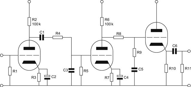
The 75 μs high frequency loss is formed by the combination of R4, R5 and C3, whereas the 3,180 μs, 318 μs pairing is formed by R8, R9 and C5. The calculation of these components is simple, but we must remember to account for hidden components such as the output resistance of the preceding valve and the Miller input capacitance of the following valve in parallel with strays.
Calculation of Component Values for 75 μs
We first note that the first and second gain stages are identical, so any calculation applied to one also applies to the other. For the DC conditions chosen for our common cathode triode input stage, ra=6 kΩ; this is in parallel with the 100 kΩ anode load resistor, so rout=5.66 kΩ.
The gain of the second stage is 29, and Cag=1.4 pF, so the Miller capacitance will be 30×1.4 pF=42 pF. In addition to this, the cathode, the heaters and the screen are at earth potential, and are in parallel with this capacitance. Cg−k+h+s=3.3 pF, and we ought to allow a few pF for external strays. A total input capacitance of 50 pF would be about right.
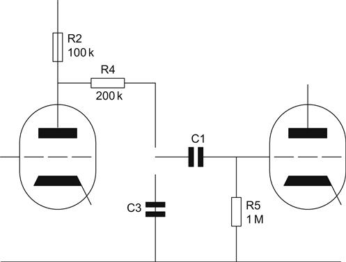
To calculate the capacitance needed for the 75 μs time constant, we need to find the total Thévenin resistance that the capacitor sees in parallel (see Figure 7.36).

For the moment, we will ignore C1, but this will be accounted for later. C3 sees the grid-leak resistor R5 in parallel with the series combination of the output resistance of the preceding valve and R4. As is usual, we will make the grid-leak as large as permissible, so R5=1 MΩ.
We are now free to choose the value of R4. We need rout to be a small proportion of R4, otherwise variations in ra will upset the accuracy of the equalisation, but too large a value of R4 would form an unnecessarily lossy potential divider in combination with R5. At high frequency, the capacitor C3 is a short circuit, and so the additional AC load on the input valve will be R4. 200 kΩ is a good value for R4, and it has the bonus of being available both in 0.1% E96 series and 1% E24 series (very few E24 values are common to the E96 series). In combination with R5, this gives an acceptable loss of 1.6 dB whilst not being an unduly onerous load for the input stage.
The capacitor now sees 200 kΩ+ 5.66 kΩ in parallel with 1 MΩ, which gives a total resistance of 170.58 kΩ. Dividing this value into 75 μs gives the total value of capacitance required, 440 pF. But this network is loaded by the second stage which already has 50 pF of input capacitance from grid to ground, so the actual capacitance that we need is 440 pF−50 pF=390 pF, so a 390 pF 1% capacitor would be fine.
We ignored the effect of the coupling capacitor C1, but this must have some effect on the Thévenin resistance seen by the capacitor. We could use a sufficiently large value to make its reactance negligible compared to the 200 kΩ series resistor, but a more elegant method is to move its position slightly (see Figure 7.37).
The capacitor now only has to be negligible compared to 1 MΩ. 75 μs corresponds to a −3 dB point of ≈2 kHz, so it is at this frequency that the values of other components are critical. At 2 kHz, a 100 nF capacitor has a reactance of ≈800 Ω, which is less than 0.1% of 1 MΩ. If we had not moved the capacitor, we would have needed a value >470 nF simply to avoid compromising RIAA accuracy.
Conversely, there is little point in using a very large coupling capacitor in an effort to reduce noise at LFs, since the 200 kΩ series resistance of R4 swamps the output resistance of the input valve and nullifies its shunting effect on the grid-leak of the second valve.
180 μs, 318 μs Equalisation and the Problem of Interaction
The second stage is direct coupled to a cathode follower in order to eliminate interaction between any coupling capacitor and the 3,180 μs, 318 μs pairing. 3,180 μs corresponds to f−3 dB=50 Hz, which is far too close to the typical 1.6 Hz cut-off resulting from 100 nF to 1 MΩ, so they would interact significantly.
The other reason for using a cathode follower is its low input capacitance, which causes an additional high frequency roll-off when placed in parallel with the 3,180 μs, 318 μs pairing. In the 75 μs network, we were able to incorporate the value of stray capacitance into our calculations, but in this instance it is not possible, so it is essential that any stray capacitance is so small that it can be ignored. The full equation for the input capacitance of a cathode follower is:
To a good approximation, Av=μ/(μ+1), so for an E88CC (μ≈32), Av=0.97, Cag=1.4 pF and Cgk=3.3 pF. The Cgk term is thus entirely negligible at 0.1 pF, so the input capacitance is virtually independent of gain at ≈8 pF, including a healthy allowance for strays to ground.
3180 μs and 318 μs Equalisation
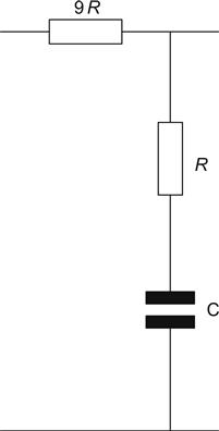
The equations that govern the 3,180 μs, 318 μs pairing are delightfully simple, CR=318×10−6, and the upper resistor=9R, whilst the loss at 1 kHz for this network is 19.05 dB (see Figure 7.38).
We should now check whether our worst case 8 pF shunt capacitance is sufficiently small not to cause a problem. To do this, we need to employ a slightly circular argument.
We first say that it will not cause any interaction. If this is true, then the frequency at which the cut-off occurs will be so high that C in the network is a short circuit. If it is a short circuit, we can replace it with a short circuit, and calculate the new Thévenin output resistance of the network. Since the ratio of the resistors is 9:1, the potential divider must have a loss of 10:1, and the output resistance is therefore one-tenth of the upper resistor. If we assume that our upper resistor will again be 200 kΩ (neglecting rout of the previous stage), the Thévenin resistance that the stray capacitance sees at high frequency is 20 kΩ; combined with 8 pF, this gives an a high frequency cut-off of 1 MHz.
As a rule of thumb, once the ratio of two interactive time constants is ≥100:1, the response error caused by interaction is inversely proportional to that ratio, so a ratio of 100:1 causes an error of ≈0.1 dB.
In our example, the ratio of 1 MHz to the nearest time constant of 318 μs (500.5 Hz) is 2,000:1, so we can safely ignore interaction and go on to calculate accurately the values for the 3,180 μs, 318 μs pairing.
If we were driving the network from a source of zero resistance, ideal values for the resistors would be 180 kΩ and 20 kΩ (perfect 9:1 ratio), since both of these are members of the E24 series, and the capacitor could then be 16 nF with only 0.6% design error. Unfortunately, our source has appreciable output resistance, so we will choose 200 kΩ as the upper resistor and must accept whatever values this generates for the lower two components.
The second stage is identical to the input stage, so output resistance is 5.66 kΩ, making a total upper resistance of 205.66 kΩ. The lower resistor will therefore be 22.85 kΩ, and the capacitor 13.92 nF. 22.85 kΩ can be made out of a 23k2 0.1% resistor in parallel with a 1M5 1%. 13.92 nF can be inconveniently made out of a pair of 6n8s in parallel with a 330 pF, or 10n in parallel with 3n9 and 20 pF. We can now draw a full diagram of the example RIAA stage with component values (see Figure 7.39).

Awkward Values and Tolerances
Equalisation networks and filters invariably generate awkward component values, and much manoeuvring is required to nudge them onto the E24 series. Sadly, this is usually wasted effort, since, although 0.1% resistors are readily available, capacitors are only readily available in 1%, and often only in E6 values. Therefore, for best accuracy, we measure the value of the largest capacitors on a precision component bridge (or perhaps a digital multimeter having an accurate capacitance range), and add an additional capacitor to achieve the required value.
For the 13.92 nF capacitor needed earlier, we might measure the 6n8 capacitors, and find that they were actually 6.74 nF, so we would actually need a 430 pF, rather than 330 pF. This is not a problem, but suppose we had chosen the more obvious 10 nF//3n9 option, but when the 10 nF 1% capacitor was measured, it was found to be 10.1 nF. We can hardly file a bit off the end!
Close tolerance components are expensive, but they are not always necessary. If we combine a close tolerance component with a looser tolerance component, then the resulting component will still be close tolerance, provided that the ratio of the values is greater than the ratio of the tolerances. Clearly, the close tolerance component must be the main component, whilst the trimming component can be looser tolerance. As an example, if we need a 22.85 kΩ resistor to a close tolerance, we could choose 23k2 0.1%, and parallel it with 1M5 1%. 1.5 MΩ/23.2 kΩ=65:1, and is greater than the 10:1 ratio of the tolerances, so this combination will be fine. Similarly, for the 13.92 nF capacitor needed earlier, the ratio of the main component to the trimming component is 16:1, so even a 430 pF 10% would be fine. We could probably only buy a 1% component, so there is no need to measure it.
Just because we have adjusted component values on test to meet our exact required value does not mean that we now have zero tolerance components. Real components drift with time and temperature, so the values will change. What we have done is to remove the initial error so that the practical value equals the calculated value, which places us in a better starting position for overall tolerance due to drift.
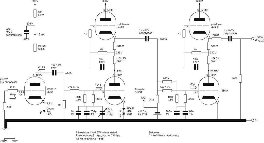
The EC8010 RIAA Stage
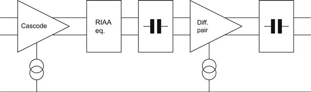
Investigating the example stage introduced the two main problems of noise and achieving accurate RIAA in the face of real-world gain stages, but gave only passing consideration to distortion. This single-ended split equalisation RIAA stage uses μ-followers to minimise distortion and transformer coupling from the moving-coil cartridge to the input stage to minimise noise and interference.
The Input Stage
The overriding requirement of the input stage is that it should produce low noise, requiring high gm, so Table 7.5 sorts valve groups by gm.
Table 7.5
| Type | Achievable gm (mA/V) |
| E810F (triode connected), EC8020 | ≈50 |
| 3A/167M, 437A | ≈42 |
| D3a | ≈34 |
| EC8010, 5842, 417A | ≈20 |
| EC86, PC86, EC88, PC88 | ≈11 |
| ECC88/6DJ8, E88CC/6922 | ≈8 |
The values given in the table are somewhat lower than manufacturers’ quoted values because they reflect usable values that can be achieved in a real design. As a very rough rule of thumb, valves designed for high gm typically achieve a mutual conductance of between one to one-and-a-half times their anode current. In other words, the E810F requires Ia≈35 mA to achieve gm≈50 mA/V, making it expensive to use, so the choice narrowed to the gm≈20 family.
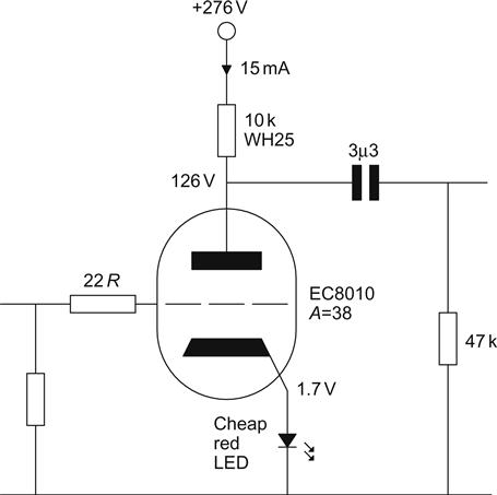
Having chosen the valve family, we must choose Ia. Since gm∝Ia, we set Ia as high as is practical, so the author chose to operate the valve at Ia≈15 mA because this current attains most of the achievable gm. We next need to choose Vgk. Many designs have set Vgk<1 V, but when the author investigated the distortion spectrum of a 5842 whilst sweeping Vgk, he found that if Vgk<1.3 V, tiny changes in bias completely changed the distortion spectrum. Once Vgk>1.5 V, the higher harmonics subsided and became stable, so the valve was biassed by a cheap red LED (setting Vgk≈1.7 V), which set Va=126 V for Ia=15 mA.
The value of the anode load RL can now be chosen. Theoretically, a high value of RL increases self-noise (![]() ), but as this is mostly attenuated by the potential divider formed by ra and RL, changing the value over an extreme range only changes the final S/N ratio by ≈1 dB. The factor that determines RL is the available HT voltage. To have a sufficiently large HT dropping resistor to allow adequate HT smoothing, we should keep the first stage HT<300 V, and since 126 V is dropped across the valve, 174 V is available for RL, so Ohm’s law determines that RL≤11.6 kΩ. RL dissipates significant power in this stage, and because a wirewound type is necessary to eliminate excess noise, the nearest E6 value of 10 kΩ was chosen. (Wirewound resistors are commonly available in E6 values only.)
), but as this is mostly attenuated by the potential divider formed by ra and RL, changing the value over an extreme range only changes the final S/N ratio by ≈1 dB. The factor that determines RL is the available HT voltage. To have a sufficiently large HT dropping resistor to allow adequate HT smoothing, we should keep the first stage HT<300 V, and since 126 V is dropped across the valve, 174 V is available for RL, so Ohm’s law determines that RL≤11.6 kΩ. RL dissipates significant power in this stage, and because a wirewound type is necessary to eliminate excess noise, the nearest E6 value of 10 kΩ was chosen. (Wirewound resistors are commonly available in E6 values only.)
We now know RL, and the current through it, so we can determine the precise HT voltage. The resistor drops 150 V, and Va=126 V, so we need 276 V of HT for the input stage (see Figure 7.40).
Once the design of the input stage had been set, it could be tested for distortion. The circuit was tested at an output of +18 dBu, which lifted the distortion harmonics clear of the noise floor but was well below clipping. Twenty-six samples were tested from the EC8010, 5842, 417A family, and they were very consistent both for total THD+N and for the individual levels of their harmonics, so a typical example is shown (see Figure 7.41).
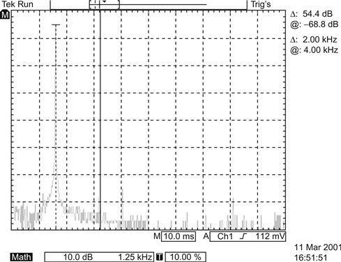
The distortion is dominated by second harmonic at −44 dB (0.65%), and the fourth harmonic is 54 dB below this at an entirely negligible −98 dB. Because distortion for a triode is proportional to level, we can predict the distortion at the proposed operating level. The nominal input sensitivity is required to be 2.5 mVRMS for 5 cm/s, and we convert this to dBu:
But we know that programme peaks will be 12 dB higher than this, so the peaks reach −50 dBu+12 dB=−38 dBu. Using an EC8010, the stage had a measured gain of 32 dB, so programme peaks at the output of the stage reach −38 dBu+32 dB=−6 dBu. We tested distortion at +18 dBu, which is 24 dB higher than −6 dBu, so the distortion at −6 dBu will be 24 dB better than that measured at +18 dBu. Thus, the distortion at −6 dBu will be −44 dB − 24 dB=−68 dB=0.04%, which is perfectly satisfactory. If we like impressive numbers, we could instead quote the distortion at the nominal 5 cm/s level, which reduces it to 0.01%.
We should next check the input capacitance of the stage. For the EC8010, Siemens specifies Cag=1.4 pF, but this will be multiplied by (1+Av) to give a Miller capacitance of 57 pF. Cin=7 pF, so the total input capacitance is 64 pF. Since the author already had the stage set up on the bench, it was easy to check this value.
Adding a resistor in series with the oscillator output produces a low-pass filter in conjunction with Cinput. The resistor value is not critical, so long as its exact value is precisely known. The filter f−3 dB point can be found by adjusting oscillator frequency until the amplitude at the output of the test stage drops by 3 dB or its phase (relative to input) changes to 135° (180°−45°). Using an 18-kΩ resistor, f−3 dB=46.9 kHz.
This is a long way away from the expected value. Since we know the gain Av of the stage, Cag can be determined using the Miller equation in reverse:
Cin is the capacitance from grid to all other electrodes, as specified by the manufacturer, plus a small allowance for strays – perhaps 2–5 pF, depending on test circuit layout.
Since the manufacturer claims Cag=1.4 pF, the value of 4.6 pF came as quite a surprise, but a direct measurement of Cag on the component bridge gave a value of ≈4.8 pF. All bridges have trouble measuring small capacitances, and the Marconi TF2700 used for this measurement was no exception. Nevertheless, the manufacturer’s claimed value for Cag is clearly hopelessly optimistic at audio frequencies.
Optimising the Input Transformer
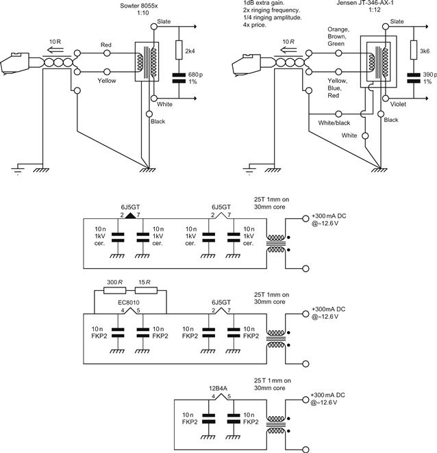
Unfortunately, 190 pF is a large shunt capacitance for the input transformer and initial square wave tests with the Sowter 8055 were very disappointing, but a Zobel network across the transformer secondary greatly improved matters. The required value of Zobel capacitance depends on cartridge DC resistance, as shown in Table 7.6.
Table 7.6
Zobel Capacitance for Sowter 8055 Moving-Coil Input Transformer when Loaded with 190 pF//6k8
| Cartridge RDC | 4 Ω | 6 Ω | 8 Ω | 10 Ω |
| CZobel | 1.5 nF | 1 nF | 910 pF | 680 pF |
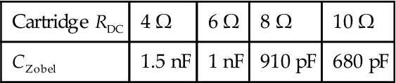
Alternatively, the Jensen JT-346-AX transformer can be used, but it is a little noisier (higher DC winding resistance). The Jensen transformer was designed for 3 Ω or 5 Ω cartridges when set to 1:12 step-up ratio, and the manufacturer’s data sheet gives appropriate Zobel values (assuming zero load capacitance). Experimentation revealed that 680 pF and 2k4 were optimum Zobel values for 11 Ω source resistance and 190 pF load capacitance.
Ultimately, the choice between transformers will probably be determined by your country of residence because buying transformers abroad is expensive. Thus, UK readers will probably opt for the Sowter, and North American readers the Jensen, whereas European readers will probably investigate Lundahl.
The Second Stage
This stage has the highest amplitude signals and therefore can be expected to produce the most distortion. As expected, when tested, gain stages with active loads such as the μ-follower and β-follower produced significantly lower distortion than a simple common cathode triode amplifier, with the further bonus of a reduced output resistance.
The μ-follower proved to be an excellent test bed for determining the irreducible distortion of a valve. The huge expansion of Internet trading means that there is now a world market for New Old Stock (NOS) valves, and almost any valve that was ever made is available somewhere. The second stage needed a valve with μ≈16, so any likely candidate was tested – together with some unlikely ones (full details in Chapter 3).
Surprisingly, given its good reputation, the 76 did not measure particularly well. Although it produced the lowest second harmonic distortion of all, its distortion was not proportional to level, and the higher-order harmonics were at a comparatively high level. Since single-ended design relies on distortion falling with level, this valve was reluctantly eliminated.
One triode was significantly better than all others. It might be packaged as a single or a dual triode, and it might have an Octal or a Loctal base, with a 6.3 V or a 12.6 V heater, but internally the valve is the same. Perhaps unsurprisingly, this valve is the 6SN7, 12SN7, 7N7, 14N7 or 6J5. The selection was further whittled down by the discovery that the metal envelope variants produced measurably higher distortion, probably due to outgassing from the hot envelope causing increased grid ion current.
Further tests revealed that the blackened glass variants such as the CV1988 (UK military 6SN7) consistently produced the lowest distortion, but that the far cheaper Pinnacle 6J5GT was very good, and selected examples equalled the CV1988. The manufacturers claim a usefully reduced Cag (3 pF compared to 3.9 pF) for the Loctals, but the main reason for choosing a Loctal would be to avoid the leakage of a phenolic base that potentially increases noise. Any of these variations on the theme would be suitable, and the final choice would probably be decided by more prosaic matters such as heater supplies, convenience of single versus dual triodes, availability of valve bases or whether you have any.
The μ-follower and β-follower were extensively tested, and the β-follower was very good, but the μ-follower had the slight advantage that it is more flexible about HT voltage, and the author wanted to ease regulator design by operating the second and third stages at the same HT voltage.
For the Pinnacle 6J5GT μ-follower, typical distortion at +28 dBu was 0.25% or −52 dB. Using this valve, programme peaks at the output of the second stage reach +12 dBu, which is 16 dB lower, so the distortion can be expected to be −52 dB−16 dB=−68 dB=0.04%, which is the same as the input stage.
Once distortion due to the lower valve in a μ-follower has been minimised, the choice of upper valve slightly affects distortion. Various valves were tried, such as triode-strapped D3a, 6C45π and Pinnacle 6J5GT. The difference in distortion between the various types was small, but the Pinnacle 6J5GT was marginally better at 8 mA than the other valves, so it was chosen.
Having found Cag of the EC8010 to be higher than expected, the Pinnacle 6J5GT was also tested. Two different measurement methods gave Cag≈5.4 pF, slightly higher than the generic value of 4 pF.
The Output Stage
The third stage has very similar output level requirements to the second stage, so another μ-follower was indicated. However, far less gain (and input capacitance) is required, so a 6J5GT is not suitable. There are very few low-μ small triodes available – the 6BX7, 6AH4 (μ=8) and 12B4-A (μ=6) are obvious choices. These valves were designed for television field scan or series regulator use, so linearity is not guaranteed. The author had considerable qualms about the decision, but eventually decided to select from his stock of 12B4-As to find a pair of low distortion samples for the output stage.
All of these low-μ valves require significant −Vgk to set optimum operating conditions, so LED bias becomes less practical, and battery bias is required if bias shift is to be avoided after overload. Again, a Pinnacle 6J5GT was chosen for the upper valve.
If the 12B4-A cannot be selected for low distortion, one possible alternative is to use an NOS 37 (μ=9) for both the second stage and the output stage. Even though a test of nine samples indicated that this valve produces double the distortion of a Pinnacle 6J5GT, its distortion was far more consistent between samples than the 12B4-A, so final performance could be better than if a pair of unselected 12B4-As had to be used.
Refining Valve Choice by Heaters
If the 12B4-A has its heaters strapped in parallel for 6.3 V (Ih=0.6 A), a stereo pair requires Ih=1.2 A. If an *SN7/*N7 is shared between the stereo channels for the second stage, it requires Ih=0.6 A. Together with the EC8010 (Ih=0.28 A), a total of 2.08 A is then required from the 6.3 V regulator. This is achievable, but a little awkward, and a pair of series 300 mA heater chains would be more convenient. Shunting the EC8010 by a 315 Ω resistance allows it to be used in a 300 mA chain; the 300 mA 6J5GT is directly suitable, and the 12B4 A can be used as a 12 V 300 mA heater, so the final line-up is EC8010, Pinnacle 6J5GT and 12B4 A.
Apart from the relaxed requirements of the heater regulator, a series heater chain has other advantages, which are detailed in Chapter 4, not least of which is reduced sensitivity to RF noise.
Choosing the Implementation of RIAA Equalisation
The EC8010 first stage has a gain of 38, resulting in an output of only 95 mVRMS at 1 kHz 5 cm/s, which is well below the 200 mVRMS decision point between split and ‘all in one go’ equalisation. Consideration of the second stage’s noise requirements if ‘all in one go’ equalisation were to be applied to a 95 mVRMS signal will quickly reinforce this decision.
We know that we will use split passive RIAA equalisation and the topology of individual gain stages. We must now choose impedances for the equalisers that give the best balance between distortion due to loading or grid current and equalisation errors due to stray capacitances and non-zero source resistances.
Grid Current Distortion and RIAA Equaliser Series Resistances
All valves source some grid current. When a valve is fed from a non-zero source impedance, its grid current develops a voltage across that impedance. Unfortunately, this voltage (which is in series with the wanted signal) is usually distorted, so it adds distortion to the wanted signal.
Passive RIAA stages must include series resistance to form their equalisers, so this provides a mechanism for grid current to introduce additional distortion. Sadly, reducing series resistance in order to reduce grid current distortion has snags:
• At frequencies when an equaliser provides maximum attenuation, the driving stage must drive a load equal to the series resistance. Reducing a stage’s load resistance steepens its loadline and increases distortion. Stages including a cathode follower, such as the proposed μ-followers, are more tolerant of loading, but caution is still needed.
• The required capacitances for the RIAA equalisers become rather large. Fortunately, 1% polypropylene capacitors are now available, but their restricted range of values and voltage ratings means that a certain amount of juggling is necessary.
From the input stage to the second stage, a 20 kΩ series resistor would have been ideal from the point of view of grid current distortion, but this loading would have reduced the gain and increased the distortion of the EC8010 input stage. On test, 47 kΩ series resistance was a suitable compromise that minimised distortion due to the two effects. Happily, the 6J5GT/6J5GT μ-follower second stage could comfortably drive 20 kΩ, making grid current distortion due to the third stage 12B4-A/6J5GT μ-follower invisible.
3180 μs, 318 μs Pairing Errors due to Miller Capacitance
In our example RIAA stage, we argued that the only logical third stage was a cathode follower because it allowed DC coupling which eliminated interaction and errors to the 3,180 μs, 318 μs pairing, and its low input capacitance avoided high frequency loss. If we could tolerate interaction, and had a means of predicting and solving the problem, then this would allow a little more freedom of design choice.
If we want to achieve levels from vinyl comparable to those from digital sources, we must increase the gain of the RIAA stage. Increasing the μ of the valve at the input or second stage causes Miller capacitance problems, so the only practical way of substantially increasing gain (without increasing the number of valves producing distortion) is to substitute a common cathode amplifier for the final cathode follower, which immediately introduces two new problems:
• The final stage must have its input AC coupled, causing interaction between the new low frequency roll-off introduced by the coupling capacitor and the 3,180 μs time constant, producing low frequency response errors.
• Because the new final stage has a gain >1, Miller capacitance becomes significant, and the equalisation network will be loaded by a far larger stray capacitance than before, causing high frequency response errors.
The 75 μs Problem
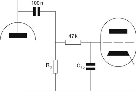
Whenever possible, extended foil polystyrene capacitors are desirable for equalisation networks since this form of construction significantly reduces ESR and series inductance. Unfortunately, commercially available types have a voltage rating of only 63 VDC, so the inter-stage coupling capacitor between the first and second stages has been forced to revert to its more traditional position, ensuring interaction with the 75 μs equalisation.
Additionally, the grid-leak resistor has been moved so that it is no longer near the grid but discharges the grid via the series resistor of the RIAA network, thus eliminating the potential divider that caused 1.6 dB loss in the basic pre-amplifier. To the author’s knowledge, the first use of this cunning trick was in Arthur Loesch’s transformerless RIAA MC stage [9] (see Figure 7.42).
The Computer Aided Design (CAD) Solution
The various interaction problems can be solved by iterative CAD AC analysis. We start by calculating values in the normal way (assuming no interaction), and then use CAD to predict the effects of interaction on frequency response using a sweep between 2 Hz and 200 kHz. Once a problem is revealed, we adjust individual component values to seek improvement. Although this sounds laborious, it can actually be quite quick, provided that we think about how, and where, we make our adjustments.
We have five variables that must be juggled to produce the correct result, so some simplification is needed. We could best start by analysing a design that does not have interaction and gently modifying it, gradually introducing interactions until we reach our final design. Alternatively, the 3,180 μs, 318 μs pairing is most affected by interaction, so we could change these components first then determine the remaining values.
3180 μs, 318 μs Pairing Manipulation
• The shelving loss at frequencies <20 Hz caused by adding the inter-stage coupling capacitor can be cured by reducing the value of the upper resistor in the potential divider.
• A mid-range shelved response (where frequencies above 1 kHz are at a constant, but different, level to those below 250 Hz) can be cured by changing the lower resistor value in the potential divider. If the higher frequencies are at too high a level, this is because the potential divider has insufficient attenuation, so the lower resistor must be reduced in value, and vice versa.
• A peak in the response centred near 500 Hz can be cured by increasing the capacitor value, whereas a dip can be cured by reducing capacitor value. This result is not quite so easily deduced, but a larger capacitor would increase the time constant, lowering the frequency at which the potential divider takes effect so that attenuation begins earlier than it should, resulting in a dip in the final response.
The last two adjustments are highly interactive, and an increase in one immediately requires a proportionate decrease (have a calculator handy) in the other to maintain the correct time constant. It is usually easiest to optimise the resistor first. The model should be tested down to 2 Hz, and the low frequency roll-off adjusted to emulate a simple 6 dB/octave filter, then optimised for minimum amplitude deviation from 20 Hz to 20 kHz.
75 μs/3.18 μs Manipulation
Although RIAA record equalisation is specified with only three time constants (3,180 μs, 318 μs and 75 μs), this would imply a 6 dB/octave rising response at the fragile cutting head. Wright [10] pointed out that at the time of cutting, RIAA pre-emphasis cannot continue indefinitely and that a final time constant of ≈3.18 μs is commonly added to prevent excessive amplitude at ultrasonic frequencies from damaging the (probably Neuman) cutting head. Unfortunately, the value of this time constant varies between cutting head manufacturers, and the less common Ortofon heads use a time constant nearer to 3.5 μs. Nevertheless, it seems reasonable to accept that an electrical 3.18 μs time constant has been deliberately added at the cutting stage in addition to the inevitable mechanical losses within the cutting heads themselves. The new replay equation is therefore:
where
This is an even more unpleasant equation than the original RIAA equation. Briefly, the effect is that instead of tending towards a 6 dB/octave low-pass filter, it tends towards ≈27.5 dB attenuation that is constant with frequency. Within the audio band, the new equaliser corrects a 0.64 dB loss at 20 kHz.
The justification for adding a 3.18 μs time constant to the replay equalisation has little to do with amplitude response, but more to do with group delay and transient response. Uncorrected, the 3.18 μs time constant changes the phase of frequencies above 5 kHz so that they no longer arrive at the same time as lower frequencies (unequal group delay), and this distorts the transient response. We cannot compensate for the cutter, and we probably don’t have the data to compensate for the cartridge response, but we can compensate for the hidden 3.18 μs time constant.
However, Yaniger convincingly argues in his ‘His Master’s Noise’ [11] article that as moving coil cartridges typically have a fierce ultrasonic tip mass resonance (which will certainly compensate for the missing time constant) and that moving-magnet cartridges don’t, only an RIAA stage intended for moving magnet cartridges should include the 3.18 μs time constant. Either way, the final time constant of 3.18 μs is physically easily included by adding a resistor in series with the capacitor producing the 75 μs time constant (see Figure 7.43).
Sadly, setting the exact value of the resistor is considerably more difficult because there are so many other high frequency roll-offs within the pre-amplifier, usually dominated by the output stage loading of the 3,180-μs, 318-μs pairing. Usually, only the additional resistor needs adjustment, but minor adjustments of the 75 μs capacitor are likely. The model should be tested up to at least 300 kHz, and finally adjusted for optimum group delay, then checked for deviations between 20 Hz and 20 kHz. It may be even necessary to make minor changes to the 3,180 μs, 318 μs pairing.
Practical RIAA Considerations
Setting the precise practical value of capacitance for the 75 μs, 3.18 μs pairing is awkward, so an Adjust On Test trimmer (AOT) is included. There are various alternatives for setting the AOT trimmer:
• Set the vanes almost half open (≈17 pF), and assume correct values for the other capacitors.
• Measure the other 75 μs, 3.18 μs capacitors on a bridge, and set the trimmer to give a predicted total capacitance of 1.35 nF, or connect them all in parallel and adjust the trimmer to give 1.35 nF.
• Measure RIAA frequency response accuracy (with a 3.18 μs capable instrument), and set the trimmer for correct response.
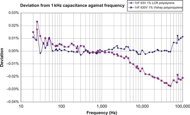
Note that the capacitance of all capacitors falls with frequency, it’s just that the defects of the better dielectrics are less visible, so although the bridge methods are indirect, they are likely to be the most accurate provided that the capacitors are polypropylene or better.
RIAA Direct Measurement Problems
Given a well-equipped laboratory, direct measurement of RIAA equalisation errors seems simple. Unfortunately, RIAA equalisation ranges from ≈+20 dB at 0 Hz to ≈−25 dB at >50 kHz, making precise measurement quite difficult.
If a constant level is applied to the RIAA stage, its level must be chosen so as to avoid overload and the measuring amplifier must accommodate the ≈45 dB range without any error. Conversely, setting the output level to be constant requires that the oscillator can set exact levels over a ≈45 dB range that can be measured precisely. Depending on the test equipment, this is either a conversion problem between the analogue and digital domains, or an analogue attenuator problem. Either way, guaranteeing attenuator error ≤0.02 dB and simultaneously a flat frequency response over a 45 dB range is not trivial and costs money.
A popular alternative is to feed the RIAA stage via a passive RIAA pre-emphasis network and measure the combined frequency response. A theoretically ideal perfect RIAA pre-emphasis network would have an output that rose indefinitely at a rate of 6 dB/octave from ≈5 kHz, but practical passive networks must have a final time constant – even if it isn’t 3.18 μs.
RIAA pre-emphasis networks are quite tricky to design, and even a perfectly designed and constructed RIAA pre-emphasis network has problems because it is sensitive to source and load impedances, which are generally considered to be constant during its design. Sadly, the carefully optimised real-world loading required by a moving magnet cartridge or a moving coil transformer disturbs the load impedance, and an incorrect oscillator source resistance would compound the problem. RIAA pre-emphasis networks should use polystyrene capacitors to avoid the slight frequency dependence of polypropylene capacitance (see Figure 7.44).
Summing up, keeping measurement errors below RIAA stage design errors is difficult.
Production Tolerances and Component Selection
Once we have optimised component values, we can test the effects of errors due to component tolerances. There is little point in specifying close tolerance components in one position if others with looser tolerances are able to upset performance.
The computer predicted the 20 Hz to 20 kHz frequency response 10,000 times, each time with random changes in all component values within their manufacturer’s tolerance. This technique is known as Monte Carlo analysis, and provided that sufficient runs are used, it predicts a likely worst case spread of frequency response. The predicted error spread for the EC8010 pre-amplifier was ±0.25 dB using the specified standard component values and without deliberate pre-selection to obtain optimum values other than setting the 75 μs, 3.18 μs trimmer capacitor to its nominal value of 17 pF.
Although RIAA errors are awkward to measure, the problem can be side-stepped by pre-selecting capacitors using a component bridge, whilst a 4½ digit DVM might even allow selection of 0.1% resistors. Even without component pre-selection, the error with new valves is likely to be well within ±0.25 dB, and pre-selection could further reduce errors.
RIAA Equalisation Errors due to Valve Tolerances
Even when a design deliberately sets out to minimise the effects of valve tolerances, the valves still dominate RIAA errors because passive components can now be so precise.
Unfortunately, rout of the input stage is a significant proportion of the series resistance that determines the 75 μs, 3.18 μs pairing. Despite this, the computer predicted an HF shelf loss of only 0.15 dB due to gm of the EC8010 falling to ⅔ of its nominal value.
As gm falls, ra rises, which reduces gain and Miller capacitance. In this design, the valves expected to affect RIAA accuracy due to changes in Miller capacitance are the second and final valves, but as they are operated as μ-followers, changes in ra do not affect gain (RL≈∞), so this mechanism is not significant.
Because rout for the μ-follower is such a small proportion of the resistance that determines the RIAA time constants, a tired valve in the upper stage of a μ-follower does not significantly affect RIAA accuracy.
This pre-amplifier’s weakness is its sensitivity to variations of Cag in the lower 6J5GT of the second μ-follower. If Cag rises by 50%, an HF shelving loss of 0.32 dB is predicted, whereas if it falls by 50%, an HF shelving boost of 0.34 dB is predicted. Happily, the pre-amplifier is immune to ±50% variations in Cag for the 12B4-A because the 20 kΩ series resistor chosen for low distortion forces low impedances in the 3,180 μs, 318 μs pairing.
Some pre-amplifiers using passive equalisation with high-μ valves, such as ECC83, have been found to sound audibly different with different makes of valve, giving rise to the belief that a Siemens ECC83 is better (or worse) than a Mullard, when it was actually differing ra and Cgk causing clear errors in RIAA equalisation.
The Balanced Hybrid RIAA Stage
The Denon DL103 moving-coil cartridge offers excellent performance for its price, so the challenge was to equalise and amplify its signal to the digital 2-VRMS standard with a similar price/performance ratio.
No Step-Up Transformers
The DL103 is an idiosyncratic cartridge to use – perhaps explaining its mixed reviews. Its low compliance means that it needs a very high mass arm having bearings that will not rattle, and its abnormally high coil resistance in combination with step-up transformer leakage inductance forms a significant low-pass filter, which means that it suffers high frequency loss unless partnered with step-up transformers each costing more than the cartridge. Having rejected step-up transformers, we now have the problem of amplifying 0.3 mVRMS at 1 kHz at 5 cm/s from a 40 Ω source with negligible hum and noise. If we ran a triode-connected E810F at full tilt, we could obtain gm=50 mA/V, resulting in an equivalent noise resistance of 50 Ω – comparable with the source. But E810Fs are expensive, and we would need 35 mA per channel of even more expensive anode current. We need a cheaper form of low-noise amplification.
Semiconductors to the Rescue
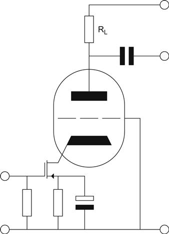
The way to obtain the required gm and therefore low noise is to use a semiconductor input device. We could make an entire semiconductor gain stage, then couple it to a valve stage, but that would be wasteful of components and involve unnecessary AC coupling. A more elegant solution is to make a hybrid cascode with the semiconductor as the lower device and the valve the upper (see Figure 7.45).
The gain of a cascode is:
To a working approximation (neglecting semiconductor output resistance), the semiconductor sees as its load the triode’s anode load RL divided by (μ+1), which implies that we can adjust the balance of the cascode’s gain structure between upper and lower devices by changing μ. A high value of μ puts more of the gain in the valve, whereas a low value shifts it towards the semiconductor.
Unfortunately, high-μ valves such as the ECC83 and 7F7 probably can’t pass enough current for the semiconductor to achieve the noise performance we require. Although we could drive additional current from elsewhere, this would be tantamount to injecting noise directly into the input stage, and no designer likes doing that. All of the semiconductor’s required current must therefore come through the valve, and that means we need the Loctal *N7 (at these signal levels, we can’t tolerate the leakage currents in the phenolic base of an *SN7). If we assume that we will need ≈3 mA and that the *N7 has ra≈6 kΩ and can tolerate a 33 kΩ load, we now know that our semiconductor sees a load of:
This is an acceptable load and suggests that it is worth continuing with the design.
Miller Capacitance
A typical LSK170C JFET can achieve gm≈15 mA/V at Ids=3 mA, so to a first approximation, the cascode gain will be:
More significantly, the gain to the valve’s cathode will be:
This is a much higher value than normal within a cascode and is a direct consequence of deliberately choosing a semiconductor having high gm. In effect, minimising noise by maximising semiconductor gm always results in high gain to the valve’s cathode, and this means that the semiconductor’s Miller capacitance (the capacitance seen looking into its input) must rise:
Worse, the capacitance of the depletion region at a reverse biassed semiconductor junction is voltage dependent:
If we want to reduce the signal dependency of our Miller capacitance, we need a reasonably large DC voltage (10 V or more) across the semiconductor. Increasing Vreverse reduces the problem of Creverse in two ways:
• A high Vreverse reduces Creverse (making it less of a problem).
• Signal swing becomes a smaller proportion of Vreverse, reducing modulation of Creverse.
You will undoubtedly have seen FET/triode cascodes where the valve’s grid is grounded, resulting in only a volt or two across the FET, implying a large and signal-dependent Miller capacitance at the FET’s gate. This might not be ideal, but it is done because the designer is terrified of injecting noise into the input stage by lifting the valve’s grid from ground.
DC Stabilisation and Consequent Gain Reduction
As soon as we include Rs to add DC feedback to stabilise DC conditions, we have also added AC feedback and reduced cascode gain. If we need to drop 100 mV whilst passing 3 mA, Rs=33 Ω, and we can calculate the effect on cascode gain if this resistor is left unbypassed:
Using the feedback equation, the cascode gain becomes:
Remembering that we want to amplify a 0.3 mVRMS signal, this translates to 100 mVRMS at the output of the cascode, which is satisfactory. We would normally fret about the effect on ra of leaving such a capacitor unbypassed, but the cascode already has near-infinite ra compared to its RL, so making it higher doesn’t make matters any worse. Nevertheless, we will have to address the cascode’s high ra problem later.
JFET Noise
The LSK170C is specified as producing 0.9 nV/√Hz at 1 kHz, so we can quickly estimate the theoretical signal-to-noise ratio of our cascode. We start by finding the equivalent noise of the LSK170C over the audio bandwidth:
We know that our cartridge produces 0.3 mVRMS, so we divide the one by the other to obtain our signal-to-noise ratio:
But we saw earlier that RIAA equalisation confers a 3.4-dB noise advantage, so the final signal-to-noise ratio is 69 dB. This quick calculation has neglected the noise generated by the cartridge’s 40 Ω winding resistance, but it’s useful because Tim de Paravacini’s rule of thumb is that the practical limit for any RIAA stage’s signal-to-noise ratio is ≈68 dB ref. 5 cm/s. Thus, the calculation suggests that our hybrid cascode input stage can’t be too far away from the practical limit.
Unfortunately, we have also neglected 1/f noise, and JFETs tend to have a 1/f noise corner somewhere between 10 Hz and 100 Hz – just where RIAA has plenty of gain. In short, 1/f noise is not negligible in this application and tends to disqualify JFETs from being used to amplify moving coil cartridges – a low-noise BJT is needed.
BJT Noise
As we saw in Chapter 3, all amplifying devices have a voltage noise source and a current noise source. Unless we’re considering capacitor microphone capsules or other capacitive sources, we can neglect current noise in FETs and valves, hence the simple 0.9 nV/√Hz JFET noise calculation. Sadly, bipolar junction transistors are not so simple, and we must calculate then sum both sources of noise.
The SSM2210 is Analog Devices’ version of the MAT02/LM394 supermatch transistor and has vn≈0.8 nV/√Hz and in≈2 pA/√Hz at 3 mA, but more significantly its 1/f noise corner is ≈1.5 Hz – below the audio band and much lower than any contemporary JFET. We calculate the voltage noise as before and obtain a figure of 113 nVRMS, but we must also calculate the noise current:
We then use Ohm’s law to find the voltage this develops across the 40 Ω source resistance of the cartridge:
This noise voltage is uncorrelated with the transistor’s noise voltage, so we must add noise powers:
In this particular instance, adding the noise due to the current source barely changed the final noise, but a higher source resistance such as a moving magnet cartridge would make a significant difference, biassing the noise argument firmly in favour of the JFET.
We divide the 114 nVRMS noise into our 0.3 mVRMS signal to find our signal-to-noise ratio as before, resulting in a figure of 70 dB once we include the 3.4 dB RIAA advantage. This calculated value of 70 dB doesn’t violate the 68 dB rule of thumb because we have neglected all other noise sources in the RIAA stage. Nevertheless, this 70 dB figure is far more likely to be credible than the JFET’s 71 dB because of the SSM2210’s low 1/f corner frequency. Irritatingly, the SSM2210 is now obsolete and has been replaced by the electrically identical SSM2212 that isn’t available in eight-pin DIP. Surface Mount Devices (SMDs) can be soldered by hand, but you need a very fine tip and <0.5 mm diameter silver-loaded solder.
Choosing between the BJT and JFET: Equalisation, Distortion and HT Power
The BJT has far higher gm than the JFET:
Therefore, cascode gain will be much higher:
This implies that there will be ≈1 VRMS leaving the first stage, rather than the 100 mVRMS calculated for the JFET version, so the immediate implication is that the JFET requires split equalisation over three stages, whereas the BJT version must use ‘all in one go’ equalisation and might only need two stages.
So far, we have not considered distortion, but cascodes are not especially linear because the lower device faces the steep loadline of the resistance looking into the valve’s cathode. Moreover, the BJT version will suffer 10 times as much distortion simply because with a fixed input signal, 10 times the gain translates into 10 times the output voltage.
Steep loadlines tend to increase second harmonic distortion, which can be cancelled by push–pull action. Thus, one way to deal with the greater distortion of the BJT version would be to configure a pair of cascodes as a differential pair. Not only would this halve the voltage on each cascode (halving the distortion), but it would also cancel the predominant second harmonic distortion. The SSM2210 comprises two NPN transistors having the defect hfe matched to ‘about 0.5%’ [12], making it particularly suitable for differential pairs.
Thus, the decision between JFET or BJT will be determined not so much by marginal noise considerations but by single-ended versus balanced considerations.
The EC8010 RIAA stage demonstrated that it is possible to obtain very low distortion in a single-ended topology, but that one part of the price is a high HT voltage (390 V) because the μ-follower is a series amplifier. 100 V of the voltage drop is due to the 10 kΩ 5 W resistors, and a β-follower could avoid that drop, bringing the HT down from ≈400 V to ≈300 V. Turning to the balanced topology, it’s very easy to not only double the component count, but also double the HT power requirement – and that’s expensive.
If a balanced topology is to be chosen, it must use the same HT power (or less) as an equivalent single-ended design and have another advantage to justify the potentially higher component count. Having become accustomed to hum-free balanced working from moving coil cartridges, the author was not keen to return to the hum problems associated with unbalanced working.
Reconciling the Balanced Decision with Practicalities
Having made the decision to adopt a balanced topology and therefore choose the SSM2210 BJT input device, the design needs to be made practical. The EC8010 RIAA stage requires 26 W from its HT, and almost half of that power is due to the need to sink 15 mA through each EC8010 input stage in order to secure low noise. Conversely, the SSM2210 produces its lowest voltage noise at Ic=3 mA, and because differential pairs are inherently low distortion, there is no need to squander HT voltage across series amplifiers. Thus, one design aim should be to reduce HT voltage and keep the current down, minimising HT power.
We have already seen that the higher gain of the BJT/triode cascode requires ‘all in one go’ equalisation, so another design aim should be to only need two gain stages.
Considering the second stage in particular, although the differential pair cancels even harmonic distortion, it would be better to minimise distortion before cancellation, and that implies maximising its ratio of RL to ra. But we need to be able to drive a cable or sound card, so a unity gain cable driver is also required. We are now able to draw a block diagram (see Figure 7.46).
Implications of the Block Diagram
In our implementation, the emitters of the SSM2210 are tied together and its bases are tied to ground, so both its transistors have the same VBE, forcing their base currents to be the same, and if their defect hFE is matched, then their collector currents must also be matched. If the triodes draw no grid current, then Ik=Ia, and all the transistors’ collector current must flow through the triodes’ anode loads, so if the anode loads are matched, the matched collector currents must result in matched anode voltages.
The significance of the previous argument is that the block diagram usefully shows us that the ‘all in one go’ equalisation can be implemented before AC coupling to the second gain stage, minimising interaction between the 3,180 μs and 318 μs time constants and the AC coupling time constant, and also enabling the use of low-voltage close tolerance capacitors for the RIAA network.
However, the diagram also shows us that the Miller capacitance of the second gain stage is across the RIAA network, so this must be taken into account during calculation. More significantly, it should be minimised (to minimise errors when it varies), suggesting that E88CC (Cag=1.4 pF) would be a better choice than *N7 (Cag=3 pF).
Another requirement highlighted by the block diagram is that we need double the usual number of coupling capacitors, so they had better not be expensive.
Since the SSM2210 bases of the BJT/triode cascode differential pair must be at 0 V (to avoid coupling capacitors to the cartridge), the emitters must be at −0.7 V, necessitating a negative supply for the tail’s CCS. Given that a subsidiary supply is already required, the ideal CCS is a cascode BJT design, which would work well from a −15 V regulated supply. An identical CCS will do very nicely for the second gain stage’s tail.
The Unity-Gain Cable Drivers
Unity-gain cable-driving ability immediately implies low distortion followers with constant current loads: either cathode followers or source followers. Further, we need AC coupling somewhere between the second gain stage and the output terminals. The alternatives are presented in Table 7.7.
Table 7.7
Comparison of Follower Alternatives
| AC coupling before followers | AC coupling after followers | |
| Cathode followers | High Vak (and therefore Pa) or subsidiary supply needed. Needs bias servo to force cathodes to 0 V | Easy biassing, ideal Vak, but elevated heaters and large coupling capacitors needed |
| Source followers | As above, but subsidiary supply could be much lower voltage | As above, but no heater supply |
As Table 7.7 shows, the advantage of AC coupling before the followers is a smaller coupling capacitor, but this is won at considerable expense. Traditionally, the expense would have been considered worthwhile because a 2.2-μF capacitor would have been large, expensive and polyethylene terephthalate. However, low voltage metallised polypropylene capacitors are now readily available, and a batch of 2.2 μF 400 V Vishay MKP1840s measured so well (low D, low ESR, constancy of C with f and high ratio of imaginary-to-real capacitance) that the author had no hesitation in choosing to AC couple after the followers.
From the point of view of sensitivity to induced interference, the ideal source resistance is zero because it equalises the (opposing) interference voltages developed by equal induced interference currents in each cable leg, enabling them to be nulled, irrespective of whether the source is balanced or not. Thus, the increased source impedance (≈1.5 kΩ as opposed to ≈100 Ω) at line frequency (50 Hz or 60 Hz) due to the series reactance of a 2.2 μF capacitor degrades hum rejection by ≈24 dB (1,500 Ω/100 Ω) in an unbalanced system. For a balanced system, any degradation is due to imbalance impedance, not absolute, so if we take the extreme of one 2.2 μF coupling capacitor being +5% and the other −5%, we have an imbalance reactance of only 76 Ω, implying that AC coupling at the output of the followers will not degrade interference suppression. Note that this argument assumes low output resistance from the followers at all frequencies.
Source followers have very slightly better distortion than cathode followers, but their main advantage is the avoidance of elevated heaters, so the author chose source followers.
Deciding the HT Voltage
The Analog Devices data sheet tells us that we need to operate the SSM2210 at 3 mA to minimise voltage noise, and this single requirement pretty well determines the rest of the entire design. We already know that we need to minimise valve Miller capacitance, so we prefer the E88CC over the 7N7, and we know that for the E88CC, Vak≈90 V is an operating point with good linearity. If we set RL=33 kΩ, then 3 mA will drop 99 V across it, and we will need an HT voltage of ≈195 V (189 V plus an allowance for Vgk).
195 V is a very significant voltage because it is comfortably within the bounds of the statistical regulator introduced in Chapter 5. This is important because a cascode’s high ra means that it has no rejection of power supply noise. Choosing a BJT lower device rather than a JFET increased the gain, and therefore the signal at the anode, reducing the effect of power supply noise, but the biggest improvement (>40 dB) came from choosing a differential topology. The combination of a simple, extremely quiet HT supply and gain stages having good common-mode rejection ratio (CMRR) enables all the stages to share a common supply, greatly simplifying the design.
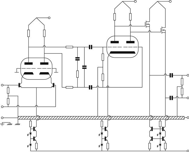
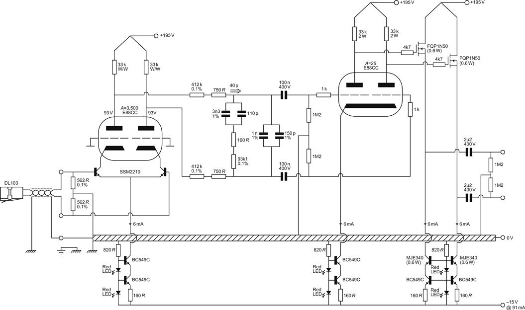
We now have enough information to be able to draw a full circuit diagram (see Figure 7.47).
Input Stage BJT Miller Capacitance
It was mentioned earlier that the semiconductor in a hybrid cascode suffers large and signal-dependent Miller capacitance unless the valve’s grid is elevated, but that doing so risks injecting noise directly into the input stage. There are two reasons why we could safely elevate the differential pair’s grids:
• Any injected noise would be common mode and rejected by the differential pair’s CMRR of >40 dB.
• The statistical regulator produces very low noise and hum, minimising injected noise.
Having deemed it safe to elevate the grids, we must decide whether we need to, and if so, by how much.
Looking up into the cathode, we see:
At 3 mA, the transistor has gm=105 mA/V, so the gain to the cathode is ≈130.
A good fit to the published SSM2210 curves of Ccb against Vcb can be obtained using:
Note that this equation has no physical significance – it just provides a good fit. Knowing Ccb and gain to the cathode, we can calculate Miller capacitance. From the E88CC curves, if Va=90 V and Ia=3 mA, Vgk≈−2.6 V, so if the grid is not elevated, Vcb=2.6 V, resulting in Cin=2,760 pF. Both halves of the differential pair have this capacitance to ground, but the cartridge is connected between the bases, so it sees these two capacitances in series, resulting in 1,380 pF seen by the cartridge. In combination with the DL103’s measured 62 μH coil inductance, this results in a resonant frequency of 540 kHz – well above the audio band, and certainly not low enough to peak the audible response.
Knowing that we will use the statistical regulator, we could conveniently elevate the valves’ grids in 5.6 V steps. If we elevate them to 11.2 V (two Zener drops), Vcb rises to 13.8 V and the cartridge sees 830 pF, which is 60% of the unelevated value, and a useful but not compelling reduction.
VCE and BJT Linearity
We know that if we don’t elevate the triodes’ grids, the collectors of the SSM2210 will be held at +2.6 V. Since their bases are at 0 V, their emitters are at −0.7 V, and VCE=3.3 V. Small-signal transistors such as the SSM2210 achieve constant current output characteristics at IC=3 mA once VCE>100 mV, and 1.3 kΩ is a comparatively shallow loadline, so we should expect to be able to swing 2 Vpk–pk without clipping at each collector. The gain of the E88CC section of the cascode would translate this to 100 Vpk–pk at each anode, or 71 VRMS between the anodes, 37 dB higher than the nominal level at this point. In short, VCE=3.3 V is perfectly adequate, there’s no need to increase it, and we can justifiably leave the triodes’ grids at 0 V.
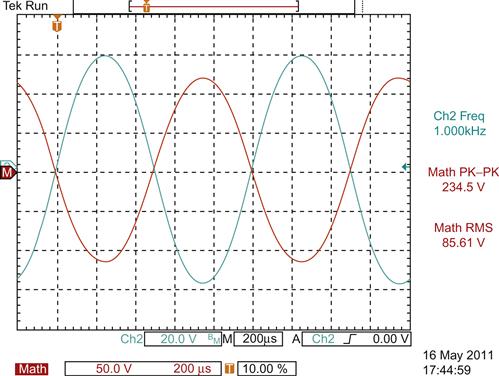
In practice, the E88CC draws grid current before the SSM2210 runs out of collector swing, further reinforcing the previous argument. Nevertheless, on test, with the triodes’ grids held at 0 V, the stage managed a very creditable maximum output of 85.61 VRMS between the anodes at 3.2% pure third harmonic distortion, just before grid current introduced even harmonic distortion (see Figure 7.48).
Backing off to 1% distortion allowed 48.17 VRMS between the anodes with an input of 13.76 mVRMS, corresponding to a 33 dB overload margin and a gain of 3,500.
Input Resistance and Bias Current
The individual amplitude against frequency response graph that comes with each DL103 shows that it was tested into a load of 1 kΩ, so this is the input resistance we should aim for. This makes sense from noise considerations as the potential divider formed by a source resistance of 40 Ω and load resistance of 1 kΩ causes an almost negligible S/N degradation of 0.34 dB, whereas the 100 Ω or greater recommended load resistance in the DL103 pamphlet would cause a ruinous 2.9 dB degradation at 100 Ω.
Unlike a valve or JFET, a BJT draws a significant bias current due to its forward biassed PN junction, and its small-signal input resistance hie loads the cartridge. The SSM2210 data sheet includes a graph of hie against IC, and at IC=3 mA, hie=4.4 kΩ. We need a DC path to 0 V from each base to allow base bias current to flow, so this resistance will be in parallel with hie. Note that because the transistors are matched and the cartridge is connected between their bases, no current flows through the cartridge.
If we want the cartridge to see 1 kΩ:
But this is the total resistance formed by the two base bias resistors in series, so each one needs to be half this value at 565 Ω, and the E24 standard value of 560 Ω will be fine.
But the base bias current flows through these resistors, and although their exact value is not critical, they should be matched to avoid generating an offset voltage that would be multiplied by the (×3,500) gain of the amplifier. Thus, 562 Ω 0.1% tolerance is a better choice.
Input Stage Noise
Although not explicitly stated, the previous noise calculations assumed a single-ended input stage with a single source of voltage and current noise, but each transistor in the differential pair is a noise source.
We saw earlier that with a source resistance of 40 Ω, the current noise source was negligible in comparison to the voltage source, so we need only consider the two voltage noise sources which are in series and equal. The signal voltage remains the same, and we add noise powers, resulting in the differential pair having a signal-to-noise ratio 3 dB worse than the equivalent single-ended stage. This is a deliberate design choice; we have bought a >40 dB hum reduction due to the differential pair’s CMRR at the expense of a 3 dB rise in random noise.
To enable direct comparison of theory and measurement, noise was measured at the output of the input stage before RIAA. With the input terminated by a 43 Ω resistor (to simulate 40 Ω DL103 source resistance plus 3 Ω arm and cable resistance), noise was measured at −61.5 dBu ± 0.5 dB (22 Hz to 22 kHz bandwidth, RMS rectifier). Referred to the 1 VRMS signal at this point, this is equivalent to −63.7 dB, and adding the 3.4 dB RIAA advantage, we have an entirely respectable S/N ratio of 67 dB. Given that the single-ended S/N ratio using the BJT was predicted to be 70 dB, and that this was expected to be degraded by 3 dB by the differential pair to 67 dB, the agreement is excellent, confirming that practical semiconductor noise matches manufacturers’ data sheets sufficiently well to enable reliable noise predictions over the audio bandwidth.
Summarising, whilst the noise performance might not be quite at the practical limit, it is satisfyingly close, and a >40 dB rejection of hum pick-up on the cabling from the cartridge should render any reasonable turntable entirely hum-free, so the author considers this to be a very worthwhile trade. Note that magnetic fields coupled directly into cartridge coils from adjacent motors or transformers are differential mode and therefore cannot be rejected.
RIAA Calculations
The equations we need are the Lipshitz equations we saw earlier:
As with split equalisation, before we can apply these equations, we must first determine our source resistance, load resistance and load capacitance.
We will treat the problem as single-ended, and as values are determined, convert them to balanced values.
To a first approximation, the output resistance of a cascode is equal to its load resistance. Strictly, we need to determine the triode’s ra:
Thus, we first need to find Rk, which for this hybrid cascode is the small-signal resistance seen looking into the SSM2210’s collector, 1/hoe. Fortunately, the SSM2210 data sheet gives a graph of small-signal output conductance (hoe) in terms of μA/V against IC, and at IC=3 mA, so we simply invert the value from the graph and find that the small-signal resistance seen looking into the collector is approximately 18 kΩ at 3 mA. At the chosen operating point, μ≈30, so:
In parallel with the 33 kΩ load resistance, this becomes 31.13 kΩ. Note that unlike the split equalisation examples seen earlier, it is RL that dominates output resistance.
The input resistance of the following stage is equal to its grid-leak resistance, which we generally arbitrarily set to 1 MΩ, but the author found that 1M2 gave more convenient capacitor values. Note that although 1M2 exceeds the Mullard data sheet’s Rgk(max) value of 1 MΩ, this is permissible because anode current runaway is prevented by the differential pair’s CCS.
There seemed no reason to choose different DC conditions for the second stage, so with RL=33 kΩ and Ia=3 mA, A=25. From the Mullard E88CC data sheet, Cag=1.4 pF, so:
This is in parallel with Cin=3.3 pF, making a round 40 pF.
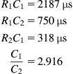
The four Lipshitz equations allow us to start anywhere, but a good place is by setting the capacitance across the input of the second stage. Remembering that we are quite restricted in capacitor values, the author chose 1 nF//150 pF between the two grids, which is equivalent to 2,300 pF from each grid to ground. The 40 pF input capacitance of each valve is in parallel with this, so the final value for the purposes of calculation is 2,340 pF. In Lipshitz’s notation, this is C1, so:
But this is the value of capacitance that would be needed for an unbalanced network, and we want balanced, so we divide by 2 to give 3.411 nF.
Using the balanced value of C1, we find the balanced value of R2 directly:
Finally, we need R1:
The calculated value of R1 is the effective series resistance seen in each leg by the equalisation network, which has the 1M2 grid-leak in parallel, so we must account for this:
But this pure series resistance includes the 31.13 kΩ output resistance of the preceding stage, so the actual series resistor we need in each leg is:
Thus, we have calculated all the component values for our RIAA network, and if we were able to DC couple to the second stage, these are the values we would use. However, we know that we need to AC couple to the 1M2 grid-leak resistors, and this must have a slight effect. The solution, as always, is to drop our calculated RIAA equaliser values, coupling capacitance, source resistance, load resistance and load capacitance into a CAD package together with the RIAA equation and iteratively adjust them until we get a flat response.
The author had some 56 nF 500 V Soviet PTFE capacitors that he wanted to use, but you might not have any, so Table 7.8 also shows values calculated for 100 nF coupling capacitors.
Table 7.8
Practical RIAA Equaliser Component Values
| 100 nF | 56 nF | |
| R1 | 412 k 0.1%+750 Ω | 412 k 0.1%+5 k 11% |
| R2 | 93k1 0.1%+160 Ω | |
| C1 | 3n3 1%+110 pF 1% | |
| C2 | 1 nF 1%+150 pF 1% | |
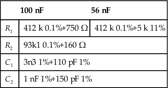
As can be seen, only R1 changed significantly with the inclusion of the coupling capacitor.
The Source Followers
The author chose FQP1N50P because he had previously bought lots of them and because earlier tests showed that they produced lower distortion than 6C45π cathode followers. We don’t expect to drive 20 m cables, so 6 mA of quiescent current per follower will be fine.
The Constant Current Sinks
The CCSs for the differential pairs’ tails are standard, using BC549C (the ‘C’ variant has a guaranteed hfe>420) to maximise their output resistance.
The source follower CCSs must dissipate 0.6 W with 100 V across them, and in the absence of CRT video driver transistors (lower output capacitance), MJE340 will have to do for the outer device. These CCSs are identical to those in the Bulwer-Lytton power amplifier, and share the LED reference chain not simply for economy, but also because it renders any noise due to the reference chain common mode, which can therefore be rejected by the next stage. Given the voltage at the followers’ sources, the CCSs could have returned their current to 0 V, rather than −15 V. However, not only would this have dirtied the 0 V, but the 14 mA required by the LEDs would have been supplied by the HT, greatly increasing required HT power.
We can now draw a full circuit diagram with component values (see Figure 7.49).
The output coupling capacitors have 1M2 resistors to ground not because such a precise value is required, but because it is convenient to use the same value as the second differential pair’s grid-leak resistors.
The HT Supply
We stated earlier that we needed 195 V, and we find that we need 48 mA of current, so we have achieved our design aim of using significantly less HT power than the EC8010 RIAA stage. We can use a single statistical regulator to power all the stages because (being balanced) each stage draws negligible signal current from the HT supply, minimising the signal voltage developed across its output impedance. To minimise interference entering the RIAA stage, the statistical regulator should be within the RIAA stage, not in the power supply. Further, for optimum LF RF rejection, the 10 μF 400 V polypropylene capacitor across the Zener chain should have a Kelvin connection (these capacitors are available from Suppression Devices of Clitheroe, UK) (see Figure 7.50).
Total Gain and Channel Balance
As configured, the RIAA stage has 5.1 dB gain in hand to match the 4 VRMS balanced digital standard from 0.3 mVRMS, and this is to allow for low-amplitude recordings.
Cartridges do not always produce matched outputs even when perfectly aligned. If required, the current programming resistor in each input stage’s CCS can be finely adjusted to correct channel balance. This works because gm=35·IC and A=gm·RL, so a change in IC directly changes gain. If such an adjustment is implemented, use fixed resistors rather than a trimmer potentiometer to avoid contact noise degrading the RIAA stage’s S/N ratio.
Summary
The balanced hybrid RIAA stage produces almost three times as much distortion as the EC8010 RIAA stage and it is third harmonic rather than second, but it costs rather less than a third of the price and has a comparable S/N ratio.
Nothing beats a well-balanced transformer for rejecting cable interference −100 dB rejection is commonly achieved. Conversely, achieving >40 dB CMRR from a practical differential pair over the 20 Hz to 20 kHz audio bandwidth requires attention to construction detail, and the rejection only holds for small interference voltages. In short, the balanced hybrid RIAA stage cannot rescue poor screening or earthing strategy, but it can put the final polish on good practice and allows the DL103 to give of its best.