
Chapter 10: Device partitioning with TrustZone
Abstract
In this chapter, we are going to look at the purpose of the TrustZone security extension and how it is implemented at the register level. Before we begin, it is necessary to define some terms that will be used throughout the chapter to avoid confusion. Like the earlier Armv7-M processors (Cortex-M3, -M4, and -M7), the Cortex-M33 has a set of operating modes that we need to review before looking at the new security states introduced by TrustZone.
Keywords
Device partitioning; TrustZone; Processor; Security extension; Programmers model; TrustZone operation; TrustZone utility
Introduction
In this chapter, we are going to look at the purpose of the TrustZone security extension and how it is implemented at the register level. Before we begin, it is necessary to define some terms that will be used throughout the chapter to avoid confusion. Like the earlier Armv7-M processors (Cortex-M3, -M4, and -M7), the Cortex-M33 has a set of operating modes that we need to review before looking at the new security states introduced by TrustZone.
Processor operating modes
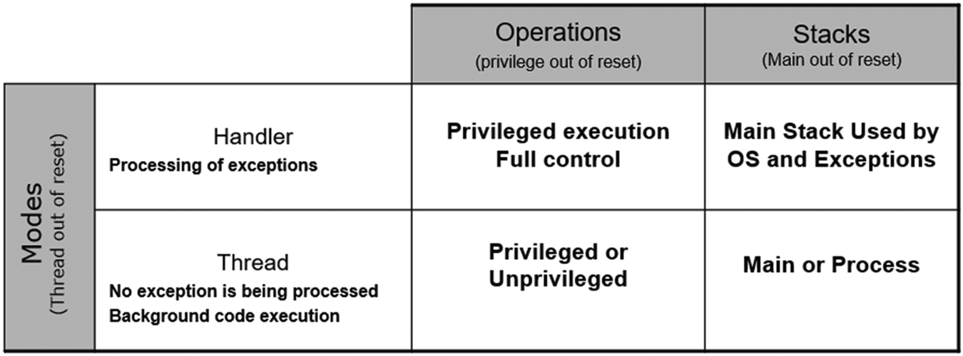
Like the Armv7-M processors, the Cortex-M33 processor has two execution modes: Handler mode and Thread mode. The processor always enters the Handler mode when an interrupt or CPU exception is raised. The processor is in the Thread state when it is executing background (noninterrupt) code. In addition to the Thread and Handler operating modes, the processor can execute code at a privileged or unprivileged level. When executing privileged code, the processor has unrestricted access to all resources and CPU instructions. However, when executing unprivileged code, the processor is more restricted, as shown in Table 10.1.
| Privileged | Unprivileged |
|---|---|
| The software can use all CPU instructions | Limited access to the MSR and MRS instructions, and cannot use the CPS instruction |
| The software can access all resources and processor registers | Cannot access the SysTick timer, NVIC, MPU, and general registers in the System Control Block |
Execution rights for privileged and unprivileged code.
After reset, the CPU has full privileged access from either Thread or Handler state. It can execute any instruction and access any region of memory. By programming the System Control Block, Control Register, it is possible to restrict the capabilities of the processor to unprivileged access when it is operating in Thread mode.
In addition to restricting the Thread mode to unprivileged access, we can also enable a second stack pointer called the process stack. After reset, the CPU R13 register is used as the main stack pointer. However, R13 is a banked register, and it is possible to enable the Process Stack pointer, again via the CPU control register. When the processor has both the main and process stacks enabled, the main stack pointer will be used by privileged code when in handler mode, while the processor stack is used by unprivileged code running in the background Thread mode. These two features can be used to create a more advanced processor configuration that is intended to support the use of an RTOS. We can extend this model by using the Memory Protection Unit (MPU) to define memory regions with privileged and unprivileged access rights. The possible processor configurations are summarized in Fig. 10.1.
TrustZone security extension
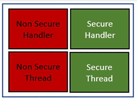
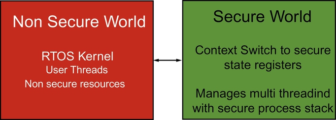
The TrustZone security extension creates additional Secure (S) and Nonsecure (NS) execution states, as shown in Fig. 10.2. These operating states are also referred to as the Secure World and Nonsecure World to reflect the fact that they are two isolated execution environments. These worlds equate to the Secure Processing Environment and Nonsecure processing Environment defined by the security model in the previous chapter.
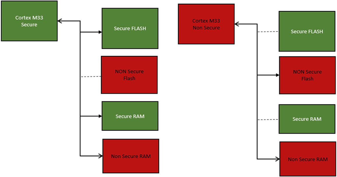
The addition of TrustZone to the Cortex-M33 will impact the processor over a number of system peripherals, as shown in Fig. 10.3. Each of these system peripherals may hold different configurations for Secure and Nonsecure World operation. This allows the CPU to have different processing environments depending on which security world is currently active. When it switches worlds, it performs a context switch to the new state. Consequently, a number of the peripheral registers are mirrored or banked between the two execution states. At the register level, this banking may be register wide or bitwise within the register. There is one exception to this scheme. TrustZone introduces a new system peripheral called the Security Attribution Unit (SAU), which is used to partition the default Cortex-M33 memory map into the separate security worlds. The SAU registers may only be accessed when the processor is executing in its secure world state.
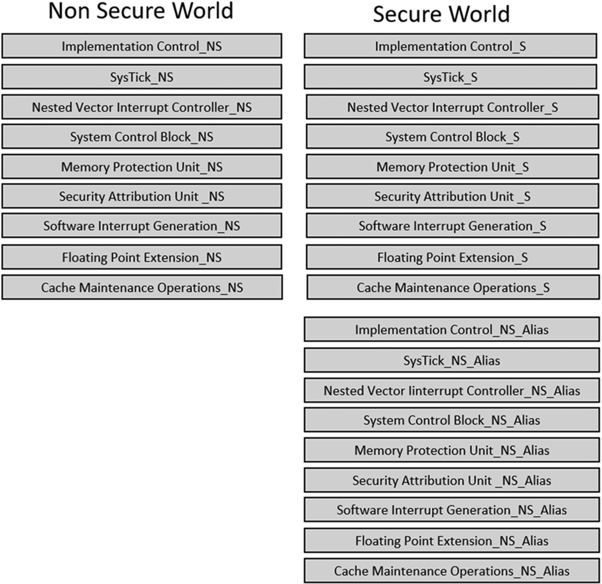
Each security partition is then fully defined by configuring its instance of the Memory Protection Unit, Nested Vector Interrupt Controller, and SysTick timer. The System Control Block also contains additional TrustZone registers and new fields within some of the default registers, which we will look at later in this chapter. In addition to the banked registers, the Secure World code is able to configure the Nonsecure World peripherals through a set of alias registers mapped into the Secure world.
Programmers model
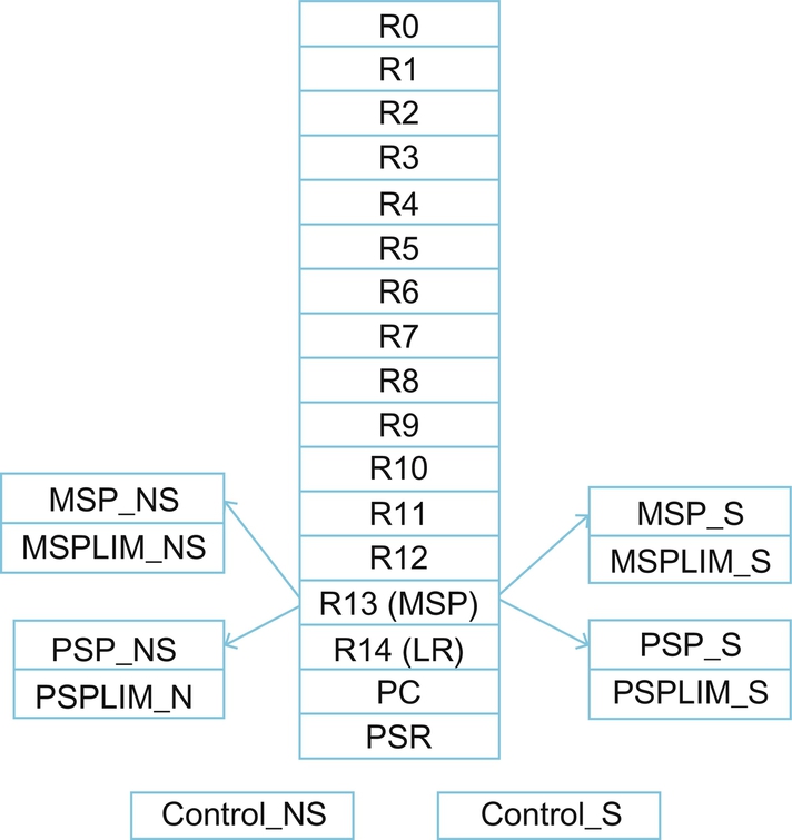
When the TrustZone security extension is fitted to the Cortex-M33 processor, the CPU programmers’ model is also updated, as shown in Fig. 10.4. While we have the same register file of sixteen 32 bit wide registers, the R13 stack pointers are duplicated to create separate main and process stack pointers for both the Secure and Nonsecure operating modes. Within the Armv8-M architecture, each of the four stack pointers has an additional stack limit register, which is used to define the lower bound of each stack region. This limit register can be updated as the code executes to actively police the stack space and mitigate against stack smashing attacks.
TrustZone operation
Before we begin to look at TrustZone in detail, it is important to understand what TrustZone is for and how it should be used. TrustZone operates at the hardware level to partitioning the processor memory map into two separate execution environments or partitions. This allows us to execute our main application in the Nonsecure World and place sensitive data and functions in the Secure World. TrustZone itself does not provide any form of encryption or other security services and does not protect against physical attacks. The purpose of TrustZone is to defend against the kind of network and software attacks discussed in Chapter 8. To understand this a bit further, we need to consider how we could design a secure system with a plain old microcontroller. In the simplest case, we could use two devices. The nonsecure code would run the bulk of the application software and provide all the real-world interfaces. The second device would contain all the sensitive software and data, such as a cryptographic library and encryption keys. The two devices are interfaced together through shared memory or a local serial bus such as SPI or I2C. When the application software requires some data to be encrypted, it would place the data into the shared memory and signal the security processor. The security processor can then encrypt the data and hand it back to the application processor. In this system, the security services are fully isolated from the application processor. While the application processor can request any available security service, it has no way to see any sensitive data or the crypto library’s internal workings. If an attacker successfully gains control of the application processor through a software attack, they have no means of reading any secure data or code as all this information is only visible to the security processor and cannot be accessed through the shared interface. The use of two processors with separated memory is an easy and well-defined way to achieve process isolation. However, it is an expensive solution, and for most applications, it is not an economic route unless you require a very high degree of security or are manufacturing in large volumes.
TrustZone is a means of achieving a similar level of process isolation at the hardware level within a single microcontroller. When the microcontroller starts, we can partition the device into two different operating modes: a Nonsecure execution mode and a Secure execution mode, as shown in Fig. 10.5.
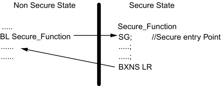
Once the SAU has been configured and enabled, the microcontroller has two distinct operating worlds that are mutually invisible to each other. In a real program, the microcontroller will startup in the secure mode and partition the device into Secure and Nonsecure Worlds. The main application code then runs in the Nonsecure partition while all sensitive code is located in the Secure partition. The two partitions can communicate by making function calls across the isolation boundary to a limited set of well-defined entry points, which are created by the addition of a new instruction to the Cortex-M33 instruction set. When a Nonsecure function calls a function located in the secure partition, as shown in Fig. 10.6, the processor will swap states. The first instruction executed in the Secure World must be a Secure Gateway (SG) instruction. If any other instruction is executed on entry to the secure world, a processor security exception is generated. Now we have two separate execution environments, and the secure code has a limited set of doorway entry points.
When the code returns from a secure function, it must use a Secure Branch Exchange or Secure Branch Link Exchange (BXNS or BLXNS) instruction (Fig. 10.7). The use of any other branch instruction to cross back to the Nonsecure partition will again raise an exception.
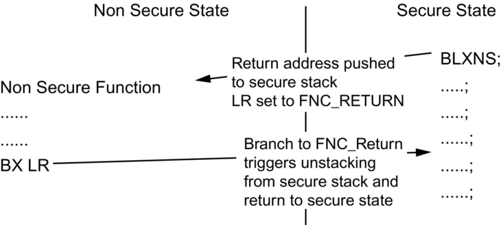
It is also possible for a function in the Secure World to call a Nonsecure function. In this case, the code will use a Branch to Nonsecure address (BLXNS or BXNS) instruction. When the stack frame is pushed, the return address to the secure code will be pushed to the secure stack, and a special code FNC_RETURN will be written to the link register. When the Nonsecure function reaches its return instruction, it will attempt to return by branching on the link register. However, the FNC_RETURN code will cause the true return address to be loaded from the secure stack along with a switch back to a secure state.
To create a fully secure execution environment, the secure world region needs to be slightly more complicated. The Secure Gateway (SG) instruction is used to provide entry points to the Secure World. However, like all instructions, the SG instruction is just a specific Boolean pattern. It would be possible for a program constant to have the same value as an SG instruction. If this happened, it would create a false entry point into the secure world, which could then be exploited by an attacker. To minimize this possibility, TrustZone does not allow a branch directly into the secure region but instead defines an intermediate region called “Secure NonSecure Callable” (NSC) (Fig. 10.8). This means the region is in the Secure World and is callable from the Nonsecure World. An attempt by the Nonsecure code to jump directly into the Secure World, bypassing the NSC region, will also cause a security exception.
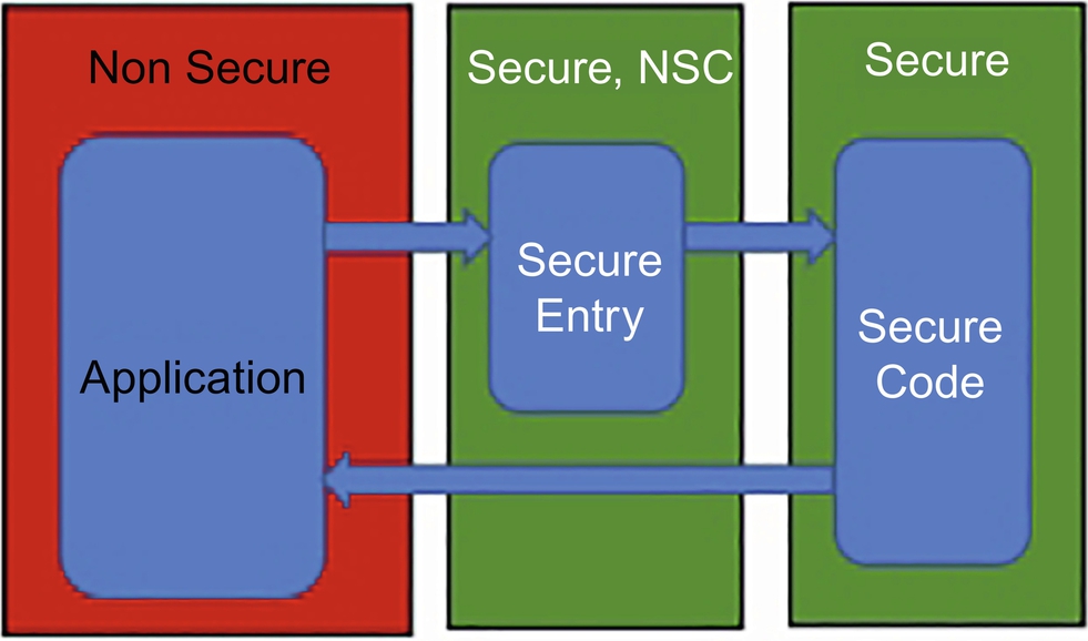
All of the SG instructions must be located in the NSC region, which acts as a stepping stone to the main Secure region. Ideally, the NSC region should only contain the SG entry points and a jump table to the security functions located in the main secure world. This makes the NSC region quite small and easy to analyze for any false entry points in the shape of a constant that looks like an SG instruction. When we create code to reside in the secure region, we also need to create a lookup table called a veneer table that provides the SG entry point. The code following the SG instruction provides an onward jump to the associated function in the Secure region. Fortunately, this process is automated by the compiler and linker and does not require you to manually maintain a low-level lookup table.
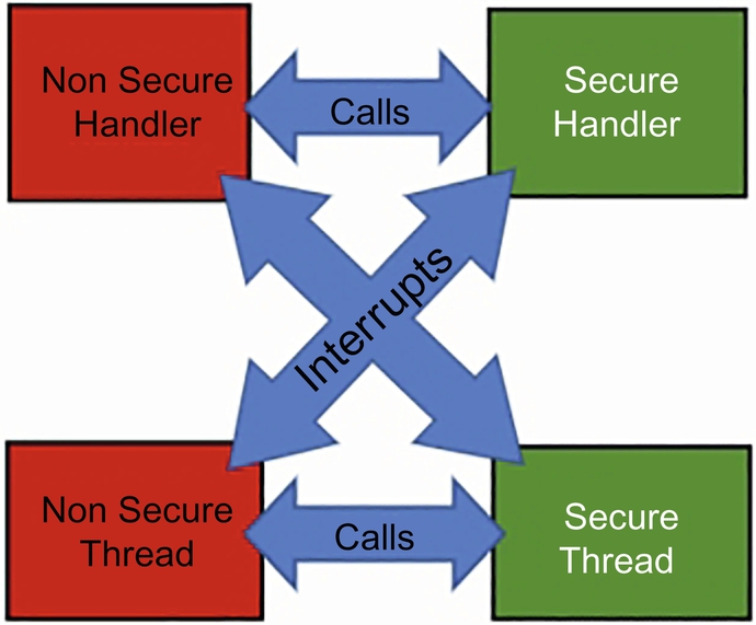
The Cortex-M33 inherits the same interrupt model that is used in Armv7-M processors. Background code runs in thread mode, and an interrupt or processor exception will cause the processor to switch into Handler mode. When TrustZone is fitted, interrupt channels can be routed to the Secure or Nonsecure NVIC so that interrupt service routines can execute in the Secure or Nonsecure world depending on the needs of the application. We will look at managing interrupts later, but for now, it is important to understand that an interrupt service routine will always be served irrespective of the current security state of the processor (Fig. 10.9). The only limitation is an overhead of 12 cycles if the processor runs in the Secure World and a Nonsecure interrupt is triggered. In this one case, the process has to stack the entire processor register file and erase the CPU registers to prevent a possible information leak before serving the interrupt. In addition to stacking the CPU registers, a signature value will also be placed on the secure stack. This is intended to prevent an attacker from faking a return from a Nonsecure interrupt. When a valid Nonsecure interrupt ends and returns to the secure world the registers will be restored provided the signature is present. In the case of a faked interrupt return the signature will not be present and a security exception will be raised.
SAU and IDAU
When the TrustZone security peripheral is added to the Cortex-M33 processor, the partitioning between the Secure and Nonsecure worlds is defined on two levels. When the device is designed, the silicon vendor will create a device level memory map that splits the resources into default Secure and Nonsecure regions that become active when TrustZone is enabled. The user can further modify this memory map by overlaying additional regions that mark the memory as Secure or Nonsecure.
This marking of the device resources is implemented by two system-level peripherals within the Cortex-M33 processor. The Security Attribution Unit (SAU) and the Implementation Defined Attribution Unit (IDAU) are used in combination to define the total security marking of the device resources (Fig. 10.10).
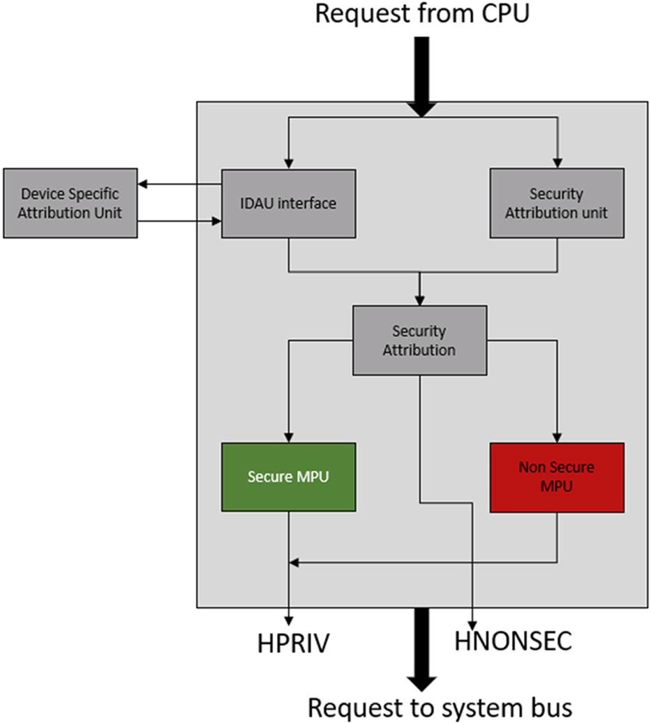
As its name implies, the Implementation Defined Attribution Unit is configured by the silicon designer when the chip is synthesized. The IDAU defines a default fixed partitioning of the Cortex-M33 address space that divides the default Cortex-M memory template into Secure and Nonsecure Regions.
A typical minimal implementation of the IDAU will divide the address space into pages of secure memory interleaved with Nonsecure memory pages. This approach is often used because it can be implemented by multiplexing bit 27–31 of the address bus to give a page size of 128 MB. This scheme creates default secure and Nonsecure Regions across FLASH memory, SRAM peripherals, and any memory-mapped external resources.
The Security Attribution Unit is then used to overlay the default IDAU memory map with additional user-defined regions. The number of regions supported by the SAU is fixed when the MCU is designed and can support two, four, or eight regions.
SAU registers
When we define the SAU regions, they will interact with the IDAU regions to create a final partitioned memory map. If either the SAU or IDAU defines a Secure region, it will take precedence over a Nonsecure or Nonsecure Callable region. Additionally, a Nonsecure Callable region will take precedence over a Nonsecure Region. These rules are summarized in Table 10.2.
| SAU state | IDAU state | Resulting state |
|---|---|---|
| Secure | Secure | Secure |
| Nonsecure | Secure | Secure |
| Secure | Nonsecure | Secure |
| Nonsecure | Nonsecure | Nonsecure |
| Nonsecure Callable | Secure | Secure |
| Nonsecure Callable | Nonsecure | Nonsecure Callable |
Memory marking between the IADU and SAU is combined to determine a final state.
The SAU is programmed through a set of memory-mapped registers, which are only accessible when the Cortex-M33 processor executes in its Secure State. Since the processor will initially start execution in Secure State, it is typical to configure the SAU and MPU at startup and then hand over to the main application running in the Nonsecure World (Table 10.3).
| Security attribution unit register | Description |
|---|---|
| SAU_CTRL | SAU Control Register |
| SAU_TYPE | SAU Type Register |
| SAU_RNR | SAU Region Number |
| SAU_RBAR | SAU Region Base Address Register |
| SAU_RLAR | SAU Region Limit Address Register |
The SAU is accessed by a set of memory mapped registers.
The SAU_Type register is a read-only register that returns the number of SAU regions implemented by the silicon vendor. You typically will not need to use this register if you are writing code for a standard MCU where the number of available regions is known in advance. However, it is useful if you are writing generic code to support a range of devices that have different numbers of SAU regions available.
By default, the SAU defines the entire address space as Secure. Each of the SAU regions are used to create Nonsecure or Nonsecure Callable areas. The SAU marking is then combined with the IDAU marking to derive a final TrustZone partitioning.
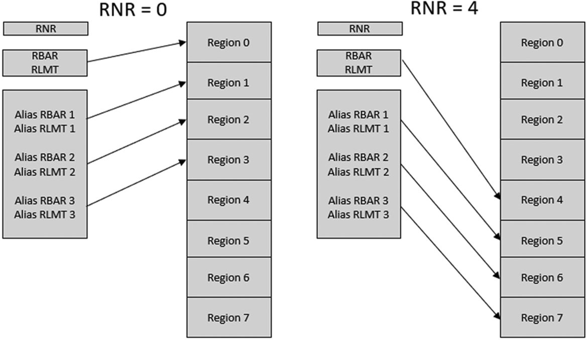
Each SAU region is configured through the Region Number Register (RNR), Region Base Address Register (RBAR), and Region Limit Address Register (RLAR). To configure a region, we first enter its number into the RNR register. The start of the region can then be entered into the RBAR. Bits 0–4 of the RBAR are reserved, so each SAU region can only be mapped to a 32-byte boundary.
The upper address of the SAU region is defined by the SAU RLAR. The upper limit address has a similar granularity to the base address register in that the first five bits of the limit address are fixed, but in the case of the RLAR, the reserved bits are set to logic one. The first two bits of the RLAR have some additional functionality. By setting bit one to logic one, the region is defined as Nonsecure Callable. Finally, the region is enabled by setting bit zero to logic one.
Although the regions are individually enabled as they are configured, they are not active until the SAU is fully enabled. When the required regions are configured and enabled, the SAU can be placed in its active state by setting bit zero in the SAU_CTRL register. The SAU_CTRL register contains one additional active bit which can be used to switch the SAU region from a default Secure marking to a default Nonsecure marking.
The example code below demonstrates creating a NSC region and a NS region.
//Configure SAU Region 0, Start Address 0x00200000, Limit //Address 0x003FFFE0, Secure nonsecure callableSAU->RNR = (0);SAU->RBAR = (0x00200000U & SAU_RBAR_BADDR_Msk);SAU->RLAR = (0x003FFFE0U & SAU_RLAR_LADDR_Msk) |((1U << SAU_RLAR_NSC_Pos) & SAU_RLAR_NSC_Msk) |1U;// Select region 1 Start Address 0x20200000 Limit Address // 0x203FFFE0 Non-SecureSAU->RNR = (1);SAU->RBAR = (0x20200000U & SAU_RBAR_BADDR_Msk);SAU->RLAR = (0x203FFFE0U & SAU_RLAR_LADDR_Msk) |((0U << SAU_RLAR_NSC_Pos) & SAU_RLAR_NSC_Msk) 1U;// Enable SAU and set the default memory marking to Non SecureSAU->CTRL = ((SAU_INIT_CTRL_ENABLE << SAU_CTRL_ENABLE_Pos) & SAU_CTRL_ENABLE_Msk)|((SAU_INIT_CTRL_ALLNS << SAU_CTRL_ALLNS_Pos) & SAU_CTRL_ALLNS_Msk);
TrustZone configuration
In this section, we will look at how a program image is created and how it executes within a microcontroller fitted with the TrustZone peripheral. There are many ways to construct a program to run using the TrustZone partitions. However, the recommended approach is to run the main application code in the Nonsecure world and treat the Secure partition as a secure enclave. This means we can place any sensitive data and functions in the secure world and make calls to them from the main application. This leads to the idea of “Security Services” provided as callable functions which are isolated from the main application along with their own Secure RAM and peripheral resources.
In the following description, we will cover the “One true way” to set up the TrustZone peripheral using a core simulator. Each silicon vendor is likely to deviate from this scheme to some extent, but once you understand the principles, you will be able to adapt to any differences. After reset, the processor will start execution in the Secure world, and we can extend the startup code (pre main()) to configure and enable the SAU. When we reach the main function in the secure code, the microcontroller resources will be partitioned between the Secure and Nonsecure worlds, as shown in Fig. 10.11.
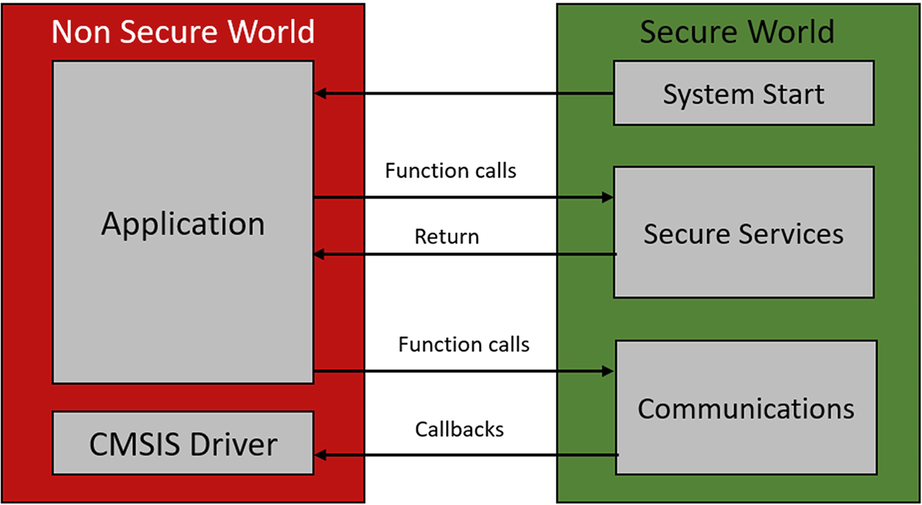
The code can then configure any secure peripherals and secure software components before leaving the Secure World and start executing code in the Nonsecure World. From this point onwards, the main user application will run in the Nonsecure World and make calls to the security services which execute in the Secure World and then return to the Nonsecure World.
The key to designing an application to execute between the Secure and Nonsecure partitions is to build two separate subprojects: one for the Secure partition and one for the Nonsecure partition. We can then provide the Nonsecure world with a table of entry points into the Secure services in the Secure partition. This allows the application code running in the Nonsecure partition to access functions in the Secure partition without having any to expose any code in the Secure project. In the next exercise, we will go through the steps required to set up both projects, but first, we will look at the overall application structure and its critical files.
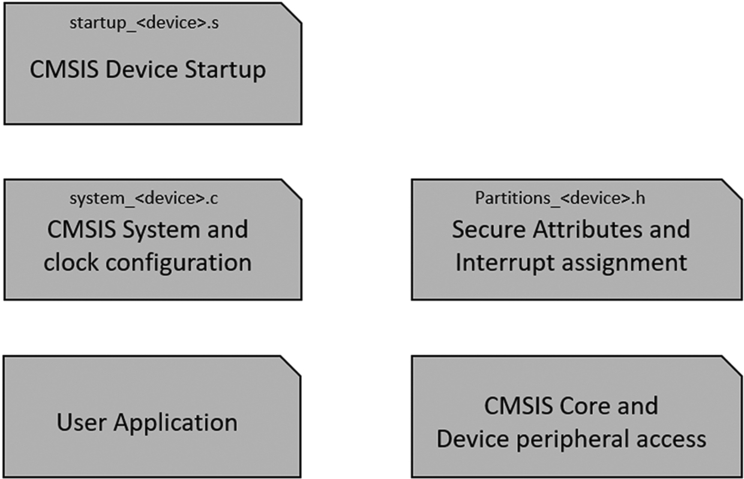
CMSIS startup files
When we create a secure project, a new file will be added to the startup folder called partition_ < device.h >. The partition header file contains a set of #defines, which are used by the system_ < device > .c file to configure and enable the TrustZone SAU peripheral at startup (Fig. 10.12).
A typical memory map will include a Secure region at the start of the FLASH memory, a Nonsecure-Callable region for the veneer table and a region of Nonsecure FLASH memory. The RAM and peripherals will also be divided into Secure and Nonsecure Regions. Once we enter the system_device.c file, the system configuration code will use some new CMSIS Core functions to configure the SAU using the partition_<device >.h header file values Table 10.4.
| Function | Description |
|---|---|
| TZ_SAU_Setup() | Configure the SAU using the definitions in partitions.h |
| TZ_SAU_Enable() | Enable the SAU |
| TZ_SAU_Disable() | Disable the SAU |
The CMSIS Core specification has been extended to provide support for TrustZone.
While the startup code is used to set up the SAU at run time, the linker scatter files for both the Secure and Nonsecure projects must also be configured to reflect this memory map (Fig. 10.13).
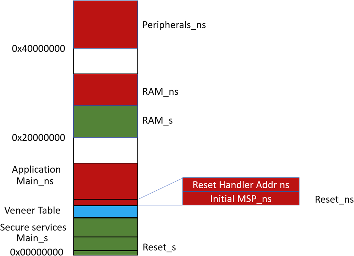
This, in effect, creates two separate executable images within the one microcontroller. The Secure image is located at the base of the FLASH memory so that it can use the processor reset vector and secure interrupt vector table. The Nonsecure image is located to an arbitrary location in the FLASH memory but is built with a standard reset handler and vector table. The transition from the Secure code to the Nonsecure code is done by performing a “software reset” in the Secure code to start execution of the Nonsecure image. The software reset loads the initial Nonsecure main stack pointer value from the start of the Nonsecure image. It then loads the address of the Nonsecure reset handler into a function pointer and then uses the function pointer to leave the Secure code and enter the Nonsecure code via its reset handler. From this point onwards, the Nonsecure code will execute like a standard application. The CMSIS core specification has been extended to provide support functions that allow the Secure code to access the Nonsecure configuration registers. This allows the Secure code to configure the Nonsecure CPU resisters during the startup phase if required.
Secure veneer functions
Once we have entered the Nonsecure code, we will need to access functions in the Secure partition. To make a Secure function visible to the Nonsecure code, we need to create a veneer table in the Secure code. We also need to provide a linkable object to the Nonsecure project so that it can make calls to the secure functions. The veneer table provides a set of SG entry points for use by the Nonsecure. To create a veneer table, we can add an attribute to a “C” function that tells the compiler it is an entry point into the Secure World. When the Secure project is built, it also creates a “dummy” library file that exports the secure gateway entry points to the Nonsecure World. This library file must be added to the Nonsecure project to provide the entry point addresses for the linker.
Exercise: TrustZone configuration
This is a multiproject workspace that contains two projects. One project will run in the TrustZone Secure-World, and one project will run in the Nonsecure World. At startup, the Secure project will configure the TrustZone SAU and then hand over to the Nonsecure code. The Nonsecure code will access functions in the Secure code. We will also trigger a security exception by making an illegal access to the secure world partition.
- In the pack installer, select Exercise 10.1 and press the Copy button.
This project uses an Arm Cortex-M33 Fast Model simulation, which allows us to experiment with the standard CMSIS-Core files. There are slight variations in approach from each silicon vendor, but once you know the standard approach, these are easy to adapt to.
- Highlight the CM33_s secure project right click and set it as the active project (Fig. 10.14).
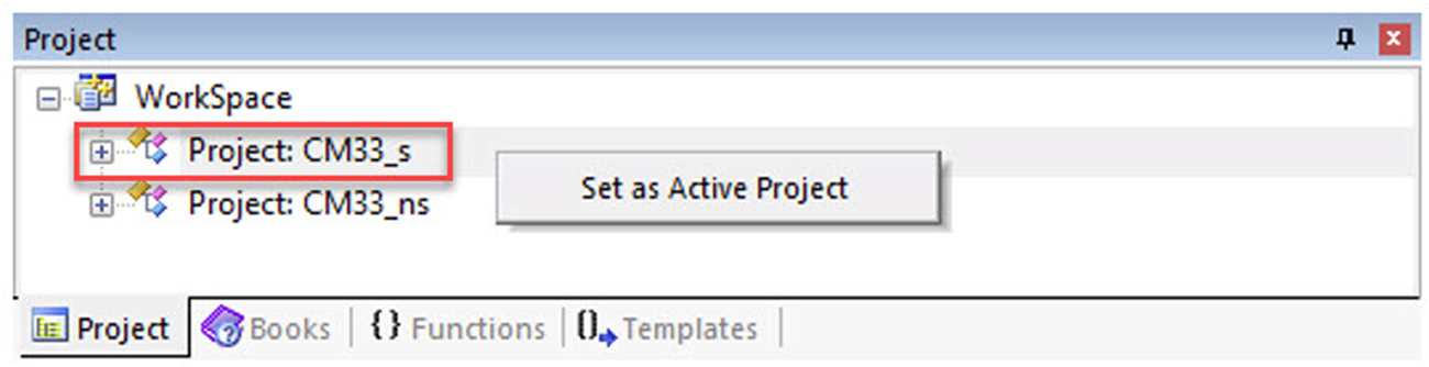
Fig. 10.14 TrustZone Workspace. The secure and nonsecure world projects are held in a multiproject workspace. No permission required.
- Open the RTE.
- Select CMSIS::Core and Device::Startup (Fig. 10.15).
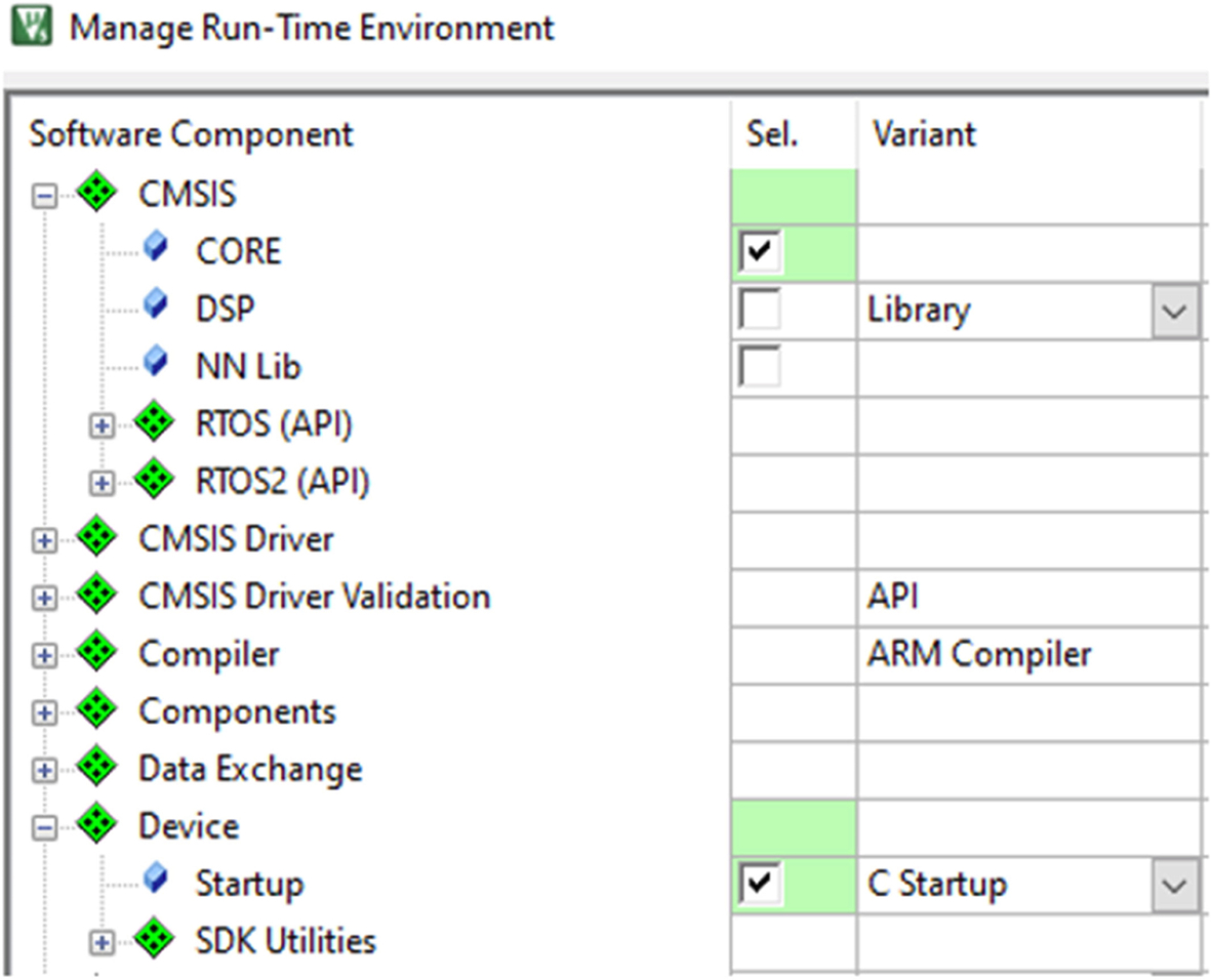
Fig. 10.15 TrustZone RTE settings. The Run Time Environment Manager adds components to the project. No permission required.
- Then click OK.
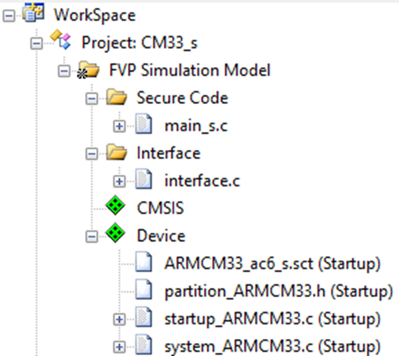
The RTE device startup option will add the low-level startup code, including the reset handler and vector table, plus the system code. Two additional files are added partition.h, which holds the configuration options for the SAU and ARMCM33_ac6.sct, which is the linker scatter file (Fig. 10.16).
- Open Partition.h.
This file is a templated file that contains configuration options to manually configure the TrustZone peripheral as shown in Fig. 10.17.
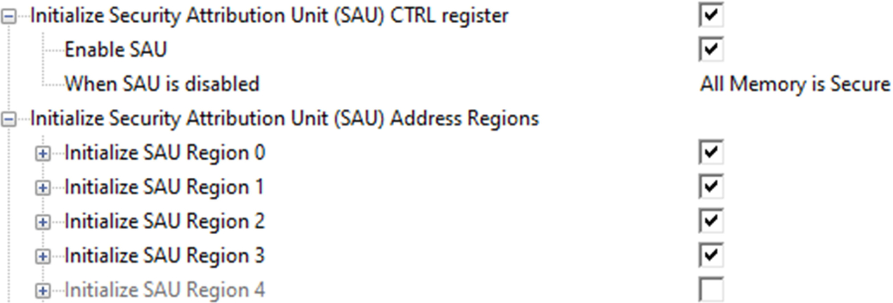
The first section of the menu allows us to enable operation of the SAU and the default access model for the memory when the SAU is disabled.
Next we can configure each of the SAU regions by defining a start and end address along with the type access allowed.
The partition.h file is preconfigured with a default memory map so don’t adjust any options for now.
- Open ARMCM33_TZ_FPU_ac6_s.sct.
The second file is the default linker file for the Secure project, as shown in Fig. 10.18. This defines the resources allocated to the Secure world executable. This should match the secure regions allocated in the partition file.
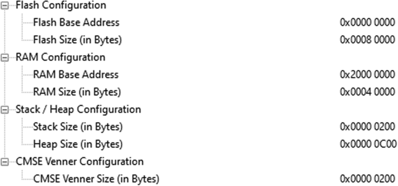
This file is preconfigured so do not adjust any options.
- Highlight the secure code folder, right click and select “Add new Item” (Fig. 10.19).
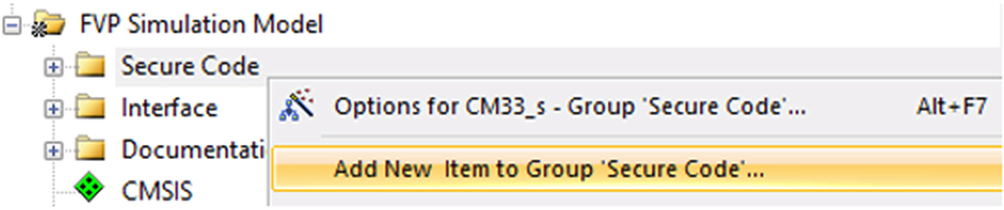
Fig. 10.19 Add a new item to the project file project file. Select the project group and right click to add a new item. No permission required.
- Select Use Code Template and add the Core: main module support file (Fig. 10.20).
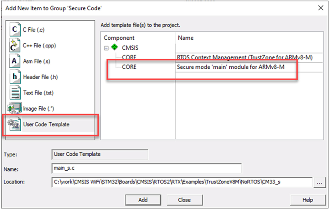
Fig. 10.20 The secure main template. A template file provides a minimal main() function. No permission required.
On startup the secure project will configure the SAU and then reach main().
Once in main() it will prepare the nonsecure project for execution by performing a software reset.
We first load the nonsecure main stack pointer with the first four bytes of the nonsecure image.
__TZ_set_MSP_NS(*((uint32_t *)(TZ_START_NS)));
The start of the nonsecure image is defined at the beginning of the main_s.c module.
#define TZ_START_NS (0x200000U)
Next we set a function pointer to the address of the nonsecure reset vector this is the image start address + 4.
NonSecure_ResetHandler = (funcptr_void)(*((uint32_t *) ((TZ_START_NS) + 4U)));
Then we can exit the secure code and jump to the start of the nonsecure code.
Execution of the Secure main() function terminates at this point. From now on, the main thread of execution will be in the Nonsecure project. The CPU will only enter into the Secure code in response to function calls from the Nonsecure code.
We can declare a function in main(), which can be called by Nonsecure code by using an attribute cmse_nonsecure_entry.
The Secure code main_s.c has an additional function to perform a simple calculation. This function uses the attribute cmse_nonsecure_entry to inform the compiler and linker that it will be called from the Nonsecure code.
We now need to configure the compiler and linker to build our Secure project.
- Highlight the project root right click and select Options for Target.
- In the target menu, change the software model to Secure Mode and select the microlib library (Fig. 10.21).
Fig. 10.21 Select secure software model. The project arget settings allows you to select the secure software model. No permission required.
Microlib is an ANSI C library that is optimized for a small microcontroller and has no specific security features.
- Next select the linker tab (Fig. 10.22).
Fig. 10.22 Secure linker settings. The linker settings are provided by a script file, which matches the TrustZone marking. No permission required.
- Uncheck the Use memory layout from target.
This will disable the auto generated linker file and instead use a custom linker file called a scatter file.
- Select the project scatter file which is in the RTEdeviceARMCM33_DSP_FP_TZ folder.
This will build the project to match the SAU settings.
We are providing functions in the Secure world which will be called from a different project running in the Nonsecure world. In order for the Nonsecure project to resolve the function symbols, we need to create a target import library that provides a symbol table and absolute address for each Secure Gateway instruction. This resolves Nonsecure function calls to functions located in the Secure partition. The target import library is created as a library object file by using the following linker directive:
--import-cmse-lib-out =<filename >
This will generate an object file that can be added to the Nonsecure code. This joins together the two separate projects to make a cohesive executable.
- Add the following line to the linker misc. controls dialog box:
--import-cmse-lib-out ="..CM33_sObjectsCM33_s_CMSE_Lib.o"
- Build the project.
As the project is built the Target Import file will also be created.
- Now set the Nonsecure project as the active project (Fig. 10.23).
Fig. 10.23 Select the Nonsecure project. Highlight and right click on the project. Then set it as active. No permission required.
- In the RTE select the CMSIS::Core and Device::Startup options then press OK.
This will add the same startup files to the project including the linker scatter file.
- Open ArmC33_ac6.sct.
- Adjust the memory mapping to match the Nonsecure regions defined in partition.h of the secure project (Fig. 10.24).
Fig. 10.24 Nonsecure linker settings. A configuration wizard helps you to easily adjust the linker settings. No permission required.
- Highlight the Nonsecure code folder, right click, and select “Add an existing file”.
- Add main_ns.c.
- Navigate to the Secure project directory and add the veneer object file CM33_s_CMSE_Lib.o (Fig. 10.25).
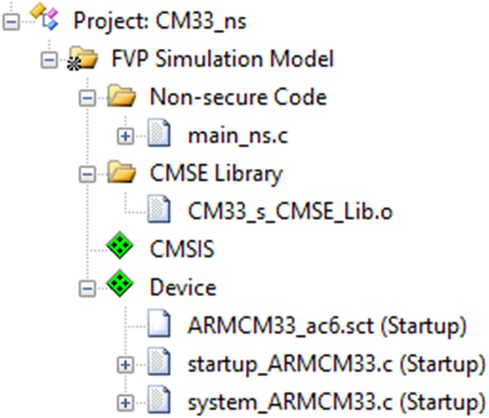
Fig. 10.25 Adding the Secure Veneer file. Add the veneer library to the Nonsecure project from its native directory. No permission required.
The veneer file is in the cm33objects directory and is called CM33_s_CMSE_Lib.o. Leave it in this location and add it to the nonsecure project in the Microvision IDE. If any memory map changes are made to the Secure project, this file will be updated in both projects.
We can now start to develop our application code. The Nonsecure main() will be the start of our application code. Here we can call Nonsecure and Secure functions. In this example code, we call a Secure function func1() to do a calculation then call another Secure function func2(). We pass a function pointer into func2(), which references a Nonsecure callback function. This will demonstrate calling a Nonsecure function from the Secure world. Finally, we set a function pointer to make an illegal call into the Secure area to demonstrate a security violation exception.
int main(void) { funcptr_void illegalFunc = (funcptr_void)(((uint32_t *) ((ILLEGAL_SECURE_ENTRY)))); val1 = func1 (1);val2 = func2 (func3, 2); illegalFunc();while (1); }
- Open the Nonsecure project options for target.
- The software model should be set to Nonsecure mode for this project and use of the MicroLIB library should be enabled (Fig. 10.26).

Fig. 10.26 Nonsecure project settings. The security model is now set to Nonsecure. No permission required.
- Switch to the compiler tab.
The Nonsecure project is accessing include files located in the Secure project.
- Add a search path into the root of the secure project ..CM33_s (Fig. 10.27).
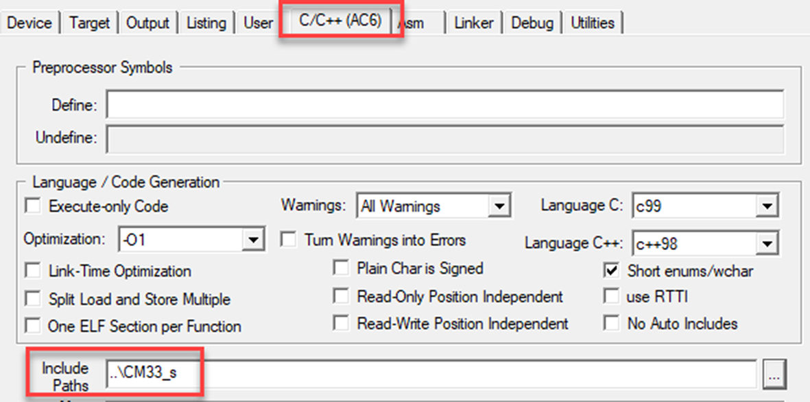
Fig. 10.27 Nonsecure compiler settings. The Nonsecure project must include a search path to the Secure project to build the veneer file. No permission required.
You can use the include path button to select the folder graphically.
- Now go to the linker tab.
- In the linker disable the “Use memory layout from Target tab.”
- Select the ARMCM33_ac6.sct scatter file in RTEDeviceARMCM33_DSP_FP_TZARMCM33_AC6.sctFig. 10.28.
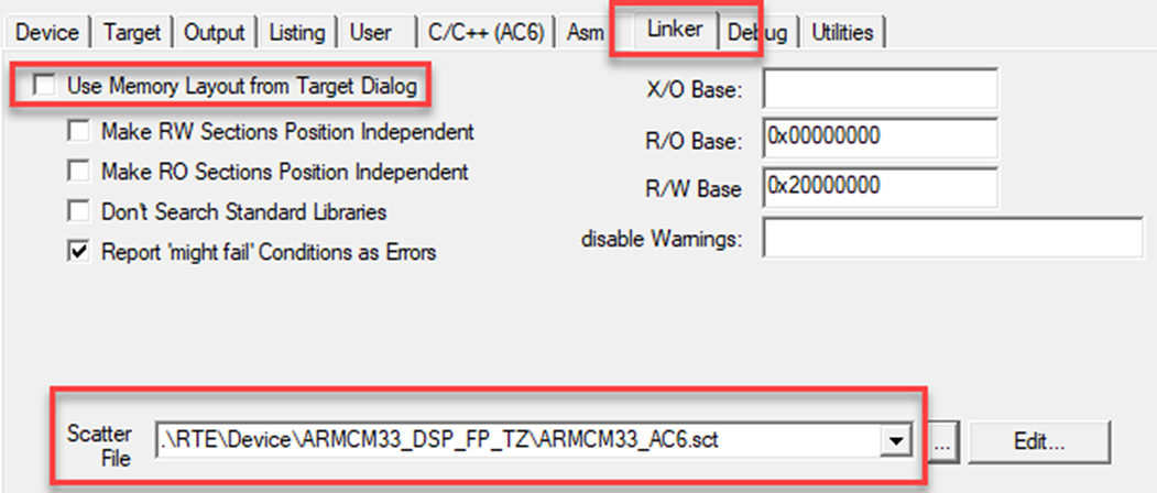
Fig. 10.28 Nonsecure linker configuration. The nonsecure project uses a matching linker script for the Nonsecure memory layout. No permission required.
- Now go to the Debug tab.
- Uncheck the load application at startup (Fig. 10.29).
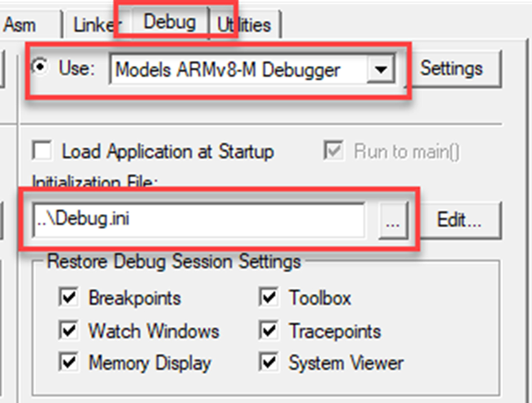
Fig. 10.29 Nonsecure debug settings. The debugger must use a script file to load both projects. No permission required.
Normally, the debugger will program the FLASH memory and load the debug symbol set when the debugger starts. In this project, we will use a script file to load both the Secure and Nonsecure images. This is done by creating an initialization file that will automatically be executed once the debugger starts.
- Press the Edit button to view the Debug.ini file.
- LOAD "..CM33_nsObjectsCM33_ns.axf" incremental
- LOAD "..CM33_sObjectsCM33_s.axf" incremental
- RESET
- g, CM33_smain_smain
The script file downloads both the Secure and Nonsecure projects into the FLASH memory and loads both symbol sets into the debugger. The “incremental” keyword means add to the existing symbol set rather than replace existing symbols with a new set. The script then resets the processor and runs the code to the secure main(). Although we have two separate images, the debugger can switch seamlessly between both sets of symbols to maintain high level debug support across both projects.
The same debug.ini file can be added to the debugger initialization box in the Secure project.
- Batch build both projects (Fig. 10.30).
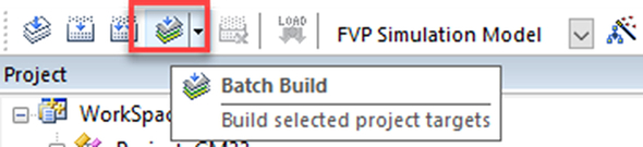
Fig. 10.30 Batch building both projects. Use the batch build icon on the toolbar to build both projects. No permission required.
The batch build option will build the Secure project first so that the import library is up to date we can then build the Nonsecure code.
- Start the debugger.
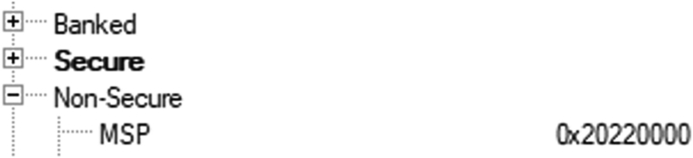
Both projects will be loaded, and the code will run to main() in the Secure project. Here, the CPU is running in Secure mode, as we can see from the register window (Fig. 10.31).
- Open the peripheralsCore PeripheralsSecurity Attribution Unit (Fig. 10.32).
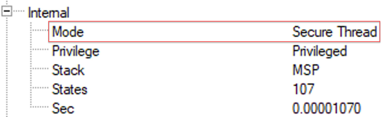
Fig. 10.31 Register view. The debugger register view displays the current active security state and operating mode. No permission required. 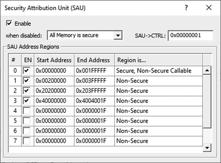
Fig. 10.32 Debug SAU peripheral view. The debugger peripheral/core peripheral view has a window for the SAU configuration. No permission required.
Here, we can see the current configuration of the SAU and can check it matches the settings defined in our partition.h file.
The Nonsecure code has also been downloaded to the FLASH memory.
- Open the viewmemory window and set the address to 0x200000 (Fig. 10.33).
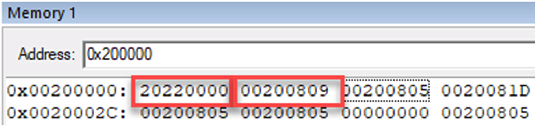
Fig. 10.33 Nonsecure memory view. Use the memory window to view the address of the Nonsecure Reset handler. No permission required.
- Right click and set the display to unsigned int.
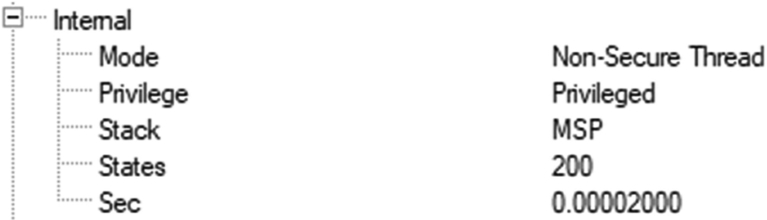
Here, we can see the first two words of the Nonsecure image. The first word is the initial main stack pointer value, and the second is the address of the reset handler.
The Secure code will load the Nonsecure MSP value into the Nonsecure R13 using a CMSIS core TrustZone function.
__TZ_set_MSP_NS(*((uint32_t *)(TZ_START_NS)));
Once this function has executed, you can see that the MSP_NS has been configured (Fig. 10.34).
Then the code will jump to the Nonsecure reset handler by executing the function pointer.
The function pointer is defined as a Nonsecure call.
typedef void (*funcptr_void) (void) __attribute__((cmse_nonsecure_call));
This will generate code that wipes the CPU registerbank and the FPU scalar registers.
Once this is done, the code will jump to the Nonsecure partition using a Nonsecure branch link exchange instruction.
Once this is executed, we will reach the Nonsecure reset handler and the CPU will be in Nonsecure mode (Fig. 10.35).
The Nonsecure code will call func1() with a Branch link instruction.
0x00200804 BL func1 (0x00000A60)
This function is in the Secure partition, so rather than jumping directly to the entry point of the function, the code jumps to the veneer table using the address provided by the import library and reaches the Secure Gateway (SG) entry instruction; this is followed by a branch to the entry point of func1().
On entry to the Secure partition the processor once again switches to Secure mode.
The function will execute a simple floating point calculation and then return to the Nonsecure code.
Before the return instruction, the compiler generates instructions to wipe the floating-point registers and then performs a Nonsecure branch exchange to return.
TrustZone access violation
The Nonsecure code also configures a rogue function pointer to an illegal entry point within the Secure partition.
- Execute theillegalFunc();call.
This will create a Secure fault which will cause the processor to switch into Secure mode and vector to the secure fault exception vector.
- Open the preipheralsCore PeripheralsNVIC (Fig. 10.36).
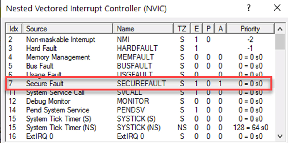
Fig. 10.36 The NVIC window in the debugger. The debugger NVIC window shows the current status of the CPU exceptions and interrupts. No permission required.
TrustZone interrupt handling
Exception vector table
When TrustZone is added to the Cortex-M33 processor, both the Secure and Nonsecure worlds have their own NVIC and a dedicated vector table. The processor exceptions are routed between the Secure and Nonsecure vector tables in three ways. They may be solely accessible by the Secure state, or they may be routed to either the Secure or Nonsecure NVIC by setting a register flag. Alternatively, an exception may be banked so that it has both a Secure and Nonsecure service routine. For example this would allow a user fault exception in both the Secure and Nonsecure Worlds (Table 10.5). Peripheral interrupts use a separate set of routing registers to select their destination as either the Secure or Nonsecure NVIC.
| Vector | Routing | Description |
|---|---|---|
| Nonmaskable Interrupt | Default: Secure State | May be routed to Nonsecure State |
| Hard Fault | Default: Secure State | May be routed to Nonsecure State |
| MemManager | Banked | Available in Secure and Nonsecure |
| Bus Fault | Default: Secure State | May be routed to Nonsecure State |
| Usage Fault | Banked | Available in Secure and Nonsecure |
| Secure Fault | Secure only | New Armv8-M TrustZone exception |
| SC Call | Banked | Available in Secure and Nonsecure |
| Debug Monitor | Implementation dependent | |
| Pend SV | Banked | Available in Secure and Nonsecure |
| SysTick | Banked | Available in Secure and Nonsecure |
| Peripheral Interrupts 0—xxx | Programmable | Routing defined by Interrupt Target Nonsecure state register |
Two processor exceptions, Reset and Security Fault, are always routed to the secure NVIC. This guarantees that any reset will force the processor into a Secure State so that it can be fully configured before the main application code can start. If there is a security fault, the processor will again be forced into the secure state so that it can log the error and run the necessary mitigation code.
The Memory Manager exception is banked so that we can provide separate service routines for the Secure and Nonsecure memory protection units.
The Supervisor Call (SVC) PEND and SYSTICK exceptions are primarily used to support an RTOS. When TrustZone is present, these exceptions are banked to allow an RTOS kernel to run in either a Secure State or Nonsecure State. We will discuss this further later in this chapter. The SYSTICK exception is slightly more complicated. If the processor is fitted with both a Secure and Nonsecure SYSTICK timer, the exception is banked. However, it is possible to have a single SYSTICK timer. In this case, the exception can be routed to either the Secure or Nonsecure processor state.
The USAGE FAULT exception is also banked. Since this exception is used to catch programming errors like divide by zero, we can usefully provide exception service routines for both Secure and Nonsecure execution errors.
The remaining processor exceptions can be routed to either the Secure or Nonsecure state. You can select their security state through the Application Interrupt and Reset Control Register (AIRC) in the Secure system control block. When the processor is fitted with TrustZone, the AIRC register has a number of additional fields, as shown in Table 10.6.
| Bits | Field | Description |
|---|---|---|
| 1 | VECTCLRACTIVE | Clear active state (for use by a debugger) |
| 2 | SYSRESETREQ | System reset request. Access depends on SYSRESETREQS |
| 3 | SYSRESETREQS | System reset state 1 = from secure state only 0 = from secure and nonsecure states. |
| 8–10 | PRIGROUP | Banked between security states. Sets interrupt priority grouping |
| 13 | BFHFNMINS | Bus Fault, Hard Fault and NMI routing 1 = Nonsecure | 0 = Secure |
| 14 | PRIS | 1 = Secure exceptions have priority | 0 = priority ranges between Secure and Nonsecure are equal |
| 15 | ENDIANNESS | Returns the Endianness of the system 0 = Little Endian | 1 = Big Endian |
| 16–31 Read | VECTKEYSTAT | You must write 0x05FA to this field when updating any other field in this register. |
| 16–31 Write | VECTKEY | On a read this field return the bit wide inverse of the VETKEY write value (0x0A05) |
By default, the selectable processor exceptions (Hard Fault, Bus Fault, and NMI) are routed to the Secure state NVIC. However, they can be routed to the Nonsecure NVIC by setting the BFHFNMINS bit to logic one. The processor Secure state has readwrite access to the BFHFNMINS bit while Nonsecure state has read-only access.
The AIRC register also contains the SYSRESETREQ bit. When set to logic one, this bit forces a processor reset. When the processor is fitted with TrustZone, an additional bit SYSRESETREQS is used to qualify which security state can write to SYSRESETREQ and reset the processor. When SYSRESETREQS is set to logic zero (default), both security states can reset the processor via SYSRESETREQ. If the SYSRESETREQS is set to logic one, the processor SYSRESETREQ can only be written to when the processor is in the Secure State.
The PRIGROUP field is used to define interrupt preemption and priority levels, but when TrustZone is present, this field is banked to allow different PRIGROUP settings in Secure and Nonsecure Worlds.
It is likely that in a real-world application, the processor will have to deal with both Secure and Nonsecure processor exceptions. At reset, the PRIS bit is set to zero, which gives equal priority to Secure and Nonsecure exceptions. If this bit is set to logic one, the Secure exceptions will be given priority over Nonsecure exceptions.
The security fault exception will also place the processor into the Secure World. The fault exceptions, hard fault and bus fault can be routed to service routines in either the Secure or Nonsecure worlds while the Usage and Memory Manager faults have banked registers that will jump to service routines in both security worlds.
Once the Secure and Nonsecure MPU’s are configured and enabled, they will generate an exception if the processor causes an access violation to an MPU region.
Finally, when writing to the AIRC register the VECTKEY field must have a write value of 0x0AF5 for the register to be updated.
Locating the nonsecure vector table
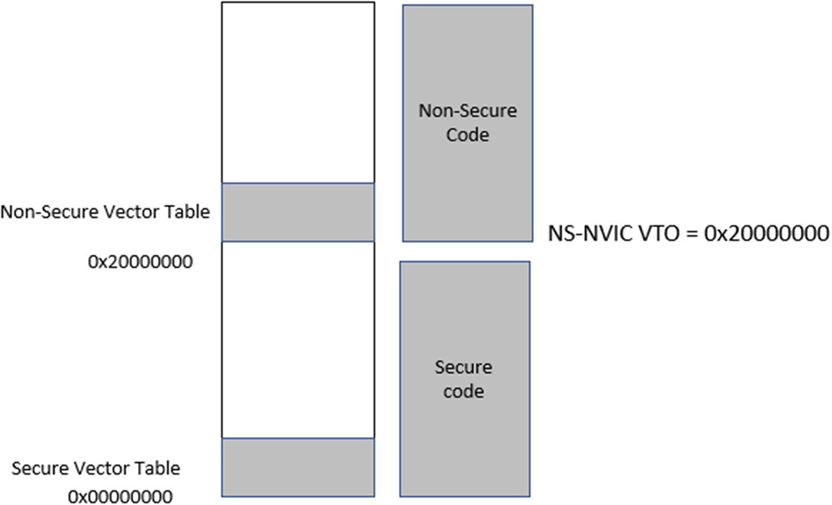
The Nonsecure code needs to perform one additional configuration before it reaches main(). The Nonsecure software vector table is programmed into the FLASH memory at the start of the Nonsecure region, but the processor Nonsecure hardware vector table is located at the beginning of FLASH memory. In order to service the Nonsecure interrupts, we need to align the Nonsecure hardware and software vector tables as shown in Fig. 10.37. This is done by programming the start address of the Nonsecure image into the Nonsecure Vector Table Offset register VTOR_NS. This is done in the Nonsecure system_init() function located in system_ < device > .c code.
Secure/nonsecure peripheral interrupt routing
The peripheral interrupt vectors grow upwards in memory from the end of the processor exception table. The Cortex-M33 can support up to 512 peripheral interrupt sources, which should keep us going for a bit. Each of these interrupt sources may be routed to either the Secure or Nonsecure NVIC. This routing is done through the NVIC “Interrupt Target Nonsecure” Registers ITENS0–15. Each peripheral interrupt channel has a dedicated bit within the ITENSxx registers, allowing each interrupt to be routed to either the Secure or Nonsecure vector table. When this bit is set to logic zero, the interrupt will be routed to the Secure NVIC. When the bit is set to logic one, the bit will be routed to the Nonsecure interrupt channel. After a processor reset, the ITENSxx registers are set to zero, routing all peripheral interrupt channels to the Secure NVIC.
Exercise: TrustZone interrupt routing
Now that we have enabled the TrustZone peripheral and partitioned the memory map using the SAU, we will also need to route the interrupt channels between the Secure and Nonsecure NVIC’s. This is done by the Secure startup code using settings for the ITNSxx registers defined in the partition.h header.
- In the pack installer, select exercise 10.2 and press the copy button.
- Open partition.h in the Secure project.
- Expand the setup Interrupt Target branch and then the Initialise ITNS 0 branch.
- Change the setting of Interrupt 1 from Secure to Nonsecure state.
- Openmain_s.c.
- Uncomment the following lines of code:
This will enable the first two interrupt channels.
The Secure and Nonsecure interrupt vector tables are defined in their respective startup files.
In the Secure code, the vector table in startup_s.c declares a vector for channel zero:
void Interrupt0_Handler (void) __attribute__ ((weak, alias("Default_ Handler")));
and an ISR function in main_s.c
- voidInterrupt0_Handler (void)
This is mirrored in the Nonsecure code for Interrupt channel 1. The interrupt vector is defined in startup.
void Interrupt1_Handler (void) __attribute__(weak, alias("Default_ Handler")));
And the ISR is created in main_ns.c.
- voidInterrupt1_Handler (void)
- Batch build the code and restart the debugger.
- Open the peripherals/core peripherals/nested vector Interrupt controller.
- Run the code so it enters the Nonsecure project.
- Openmain_ns.c.
- Set a breakpoint on the entry tovoidInterrupt1_Handler (void) line 52.
- In the NVIC window select ExtIRQ 1.
- Set the Pending bit in the “Select Interrupt” panelFig. 10.38.
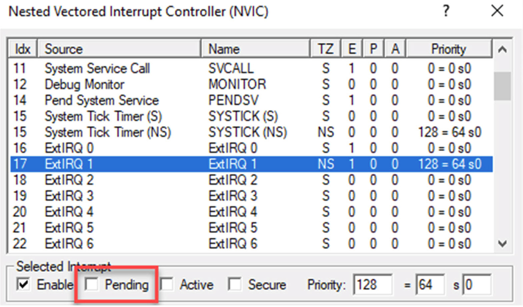
Fig. 10.38 NVIC interrupt routing. The debugger NVIC window shows the interrupt current state. We can also simulate a pending interrupt. No permission required.
- Run the code.
This will simulate an interrupt on NVIC channel 1 which will be routed to the ISR handler in the Nonsecure code.
- Now set a breakpoint on the secure ISR in main_s.c.
- Run the code and trigger an interrupt by setting the NVIC pending bit for ExtIRQ0.
The channel 0 interrupt will be routed to the ISR handler in the Secure code.
TrustZone system control block
The system control block registers are also modified when TrustZone is fitted with the Cortex-M33 processor. TrustZone adds some new registers and additional bit fields in existing registers. The SCB registers are selectively banked between the Secure and Nonsecure state. In addition, there is an alias region for the Nonsecure SCB, which allows the Secure world to configure the Nonsecure world SCB registers. A summary is shown in Table 10.7.
| Register | Banked between states? | Contains TrustZone fields | Notes |
|---|---|---|---|
| Interrupt Control and State Register | Bitwise | ✓ | NS World access to some exception bits is controlled by the AIRCR.BFHFNMINS bit |
| Vector Table Offset Register | ✓ | ✖ | Write Access is implementation defined |
| Application Interrupt and Reset Control Register | Bitwise | ✓ | May elevate priority of Secure interrupts over Nonsecure interrupts. Defines if a software reset may be executed from Secure world only. Hard fault, bus fault and NMI may be Secure world only (BFHFNMINS = 0) |
| System Control Register | Bitwise | ✓ | Configures SLEEPDEEP and SEVONPEND options for a given security state |
| Configuration and Control Register | ✓ | ✓ | The configuration flags a banked between security states |
| System Handler Priority Register 1–3 | Bitwise | ✓ | Processor exception priority fields. These will be banked to match the routing of the CPU exceptions as discussed in section. |
| System Handler Control and State Register | Bitwise | ✓ | CPU exception status flags. These will be banked to match the routing of the CPU exceptions as discussed in section. |
| Configurable Fault Status Register | Bitwise | ✓ | |
| MemManage Fault Status Register | ✓ | ✖ | |
| BusFault Status Register | ✖ | ✖ | Provides Bus Fault error flags |
| UsageFault Status Register | ✓ | ✖ | Provides Usage Fault error flags |
| HardFault Status Register | ✖ | ✖ | Provides hard Fault error flags |
| MemManage Fault Address Register | ✓ | ✖ | Provides Memory manager fault address |
| BusFault Address Register | ✖ | ✖ | Provides Bus Fault address |
| Auxiliary Fault Status Register | ✖ | Implementation Defined | May contain nonstandard vendor specific flags |
| Co Processor Access Control | ✓ | ✖ | Defines privileged/unprivileged access rights for Co Processors 0–07, Defines access rights for the floating point unit as Co Processor 10–11 |
| Nonsecure Access Control | ✖ | ✓ | Defines Nonsecure access permission for co processor 0–7 and Floating point Unit as Co Processor 10–11 |
Additional TrustZone fields are added to the SCB registers which may also be banked between security worlds.
A full description of the SCB registers is provided in the Armv8-M architectural manual. However, it is worth noting that the BHFHFNMINS bit in the AIRCR is set to logic one, then the visibility of some bits will be limited to the Secure world.
SysTick
When TrustZone is fitted to the Cortex-M33 processor, the silicon designer has a number of choices on how to implement the SysTick timer. It is possible to have zero, one or two SysTick timers. In the case of dual timers, each security mode has an independent SysTick timer, and the SysTick exception is banked, providing a dedicated interrupt for each security mode. If a single SysTick timer is present, it may be owned by either security state depending on the state of the STTNS (SysTick Targets Nonsecure) bit in the Interrupt Control and State ICS register.
The CMSIS core specification provides a standard function to enable the SysTick exception and configure its countdown period. This function can be used in either security mode to configure the local timer. An additional function is also provided, which allows the Secure mode to configure the Nonsecure SysTick timer, as shown in Table 10.8.
| Function | Security state | Description |
|---|---|---|
| uint32_t SysTick_Config (uint32_t ticks) | Secure or Nonsecure | Configures the SysTick timer for the active security state |
| uint32_t TZ_SysTick_Config_NS(uint32_t ticks) | Secure | Configures the Nonsecure SyTick timer from the Secure state |
The CMSIS SysTick timer functions are extended to include access to the secure alias registers.
Exercise: TrustZone SysTick support
The simulation model implements both the Secure and Nonsecure SysTick timers. This allows us to extend our example to enable both timers and generate interrupts in both the Secure and Nonsecure Worlds.
- In the pack installer select and copy exercise 10.3.
- Open main_s.c.
- Uncomment the following lines:
This will enable both the Secure and Nonsecure SysTick timers.
- Batch build the code and start the debugger.
When each SysTick reaches count zero an exception is generated and will be routed to a handler in the matching security mode.
- In main_s.c locate the ISR handler SysTick_Handler() and set a breakpoint at the start of the function.
- Open main_ns.c and set a breakpoint on the nonsecure SysTick_Handler() function.
- Run the code.
As each timer generates an exception the debugger will halt at the matching ISR routine.
Using an RTOS with TrustZone
When we are using an RTOS with a Cortex-M33 fitted with TrustZone, we have to decide if the RTOS kernel will be located in the Secure world or the Nonsecure world. While it is possible to locate the RTOS kernel in either partition, the recommended option is to place the kernel in the Nonsecure partition (Fig. 10.39). The RTOS does not contain any sensitive code, so it does not really need to be placed in the secure partition. We also want to keep the complexity and size of the secure code as low as possible. Furthermore, we do not want to do a field update of the secure partition unless absolutely necessary and placing the RTOS kernel in the Nonsecure world allows us to update the RTOS at will. Keeping the RTOS kernel in the Nonsecure partition also allows existing Cortex-M RTOS implementations to port easily to the Armv8-M architecture. Therefore, the RTOS kernel is best located in the Nonsecure partition, but there are still some issues that we need to address.
Multi-threaded access to secure functions
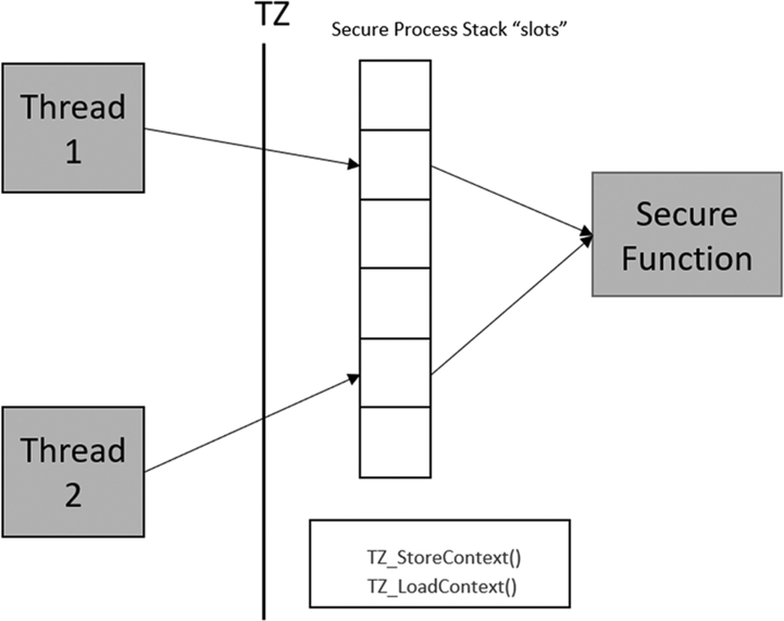
When we use an RTOS, the Nonsecure code will be running as RTOS threads. Several different threads may need to make calls to functions in the Secure world. This leads to the problem that one thread could call a Secure function and before the Secure function returns, there is a task switch, and the Secure function is called again by the newly active thread. Since the Secure partition does not access the Nonsecure RAM, the Secure function cannot use the active thread stack memory. Effectively, the Secure world functions are single-threaded and use a common region of RAM. If we have multiple calls to the Secure function, this Secure RAM will be corrupted. To solve this problem, we need to provide some additional functions within the Secure partition that provide dedicated memory for each call to the Secure function. It is also important to standardize this context management, so any firmware designed to run in the Secure partition can be used with any RTOS.
CMSIS core TrustZone functions
The CMSIS core specification has been extended to provide a set of context management functions that can be used by any RTOS, as shown in Table 10.9. These functions are used to divide the Secure process stack into a number of slots. When a thread calls a Secure function, it is allocated a process stack slot which will be used as working memory by the secure function.
| Function | Description |
|---|---|
| uint32_t TZ_InitContextSystem_S (void) | Initialize stack memory and context management |
| TZ_MemoryId_t TZ_AllocModuleContext_S (TZ_ModuleId_t module) | Allocate secure memory for a given thread |
| uint32_t TZ_FreeModuleContext_S(TZ_MemoryId_t id) | Free the context memory |
| uint32_t TZ_LoadContext_S (TZ_MemoryId_t id) | Load the new thread context during a task switch |
| uint32_t TZ_StoreContext_S(TZ_MemoryId_t id) | Store the current context during a task switch |
The CMSIS core specification now include support for TruztZone context management.
When the RTOS starts, it will call the TZ_InitContextSystem_S (), which will initialize the context management and secure stack. The context functions divide the process stack space into blocks of memory termed slots. As we create threads in the Nonsecure World, their run-time parameters are defined by a thread attribute structure. This structure includes a TrustZone Module identifier. This identifier should be set to logic one for any thread that will access Secure functions and logic zero if the thread will only be used for Nonsecure code. As the thread is created, it will call the TZ_AllocModuleContext_S() function, which will define the Secure runtime stack slot for that thread. During runtime, the Secure stack slots are managed by two functions which are used to load and store the current context. When a task switch occurs, the current thread context will be stored into the stack slot using TZ_StoreContext(), and the new thread context will be loaded using the TZ_LoadContext() function to assign a new stack slot and thread memory ID (Fig. 10.40).
Each of these functions are only a few lines of code, so do not impose any real overhead on the processor. We can see this in action in the next example.
Exercise: Using an RTOS with TrustZone
In this exercise, we will add an RTOS and secure function context management to the last project. The application code has been modified to start the RTOS and call the Secure functions via multiple threads.
- In the pack installer select Exercise 10.4 and press the Copy button.
- Set the secure project as the active project (Fig. 10.41).
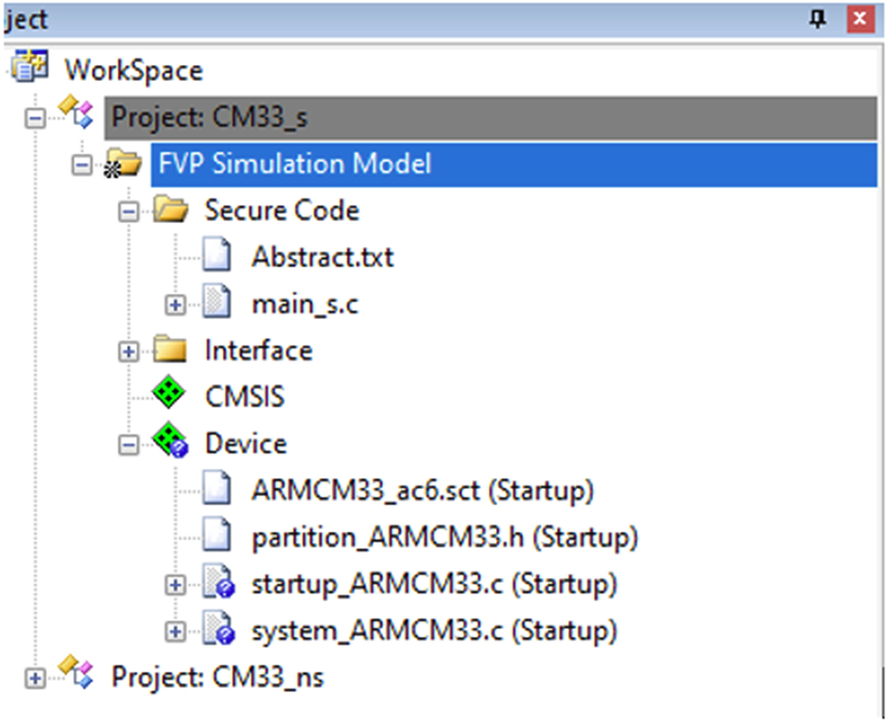
Fig. 10.41 RTOS project workspace. Open the workspace and set the secure project as the active project. No permission required.
- Highlight the interface folder right click and select “Add new Item.”
- Select the user code template.
- Add the CMSIS core RTOS context management tz_context.c (Fig. 10.42).
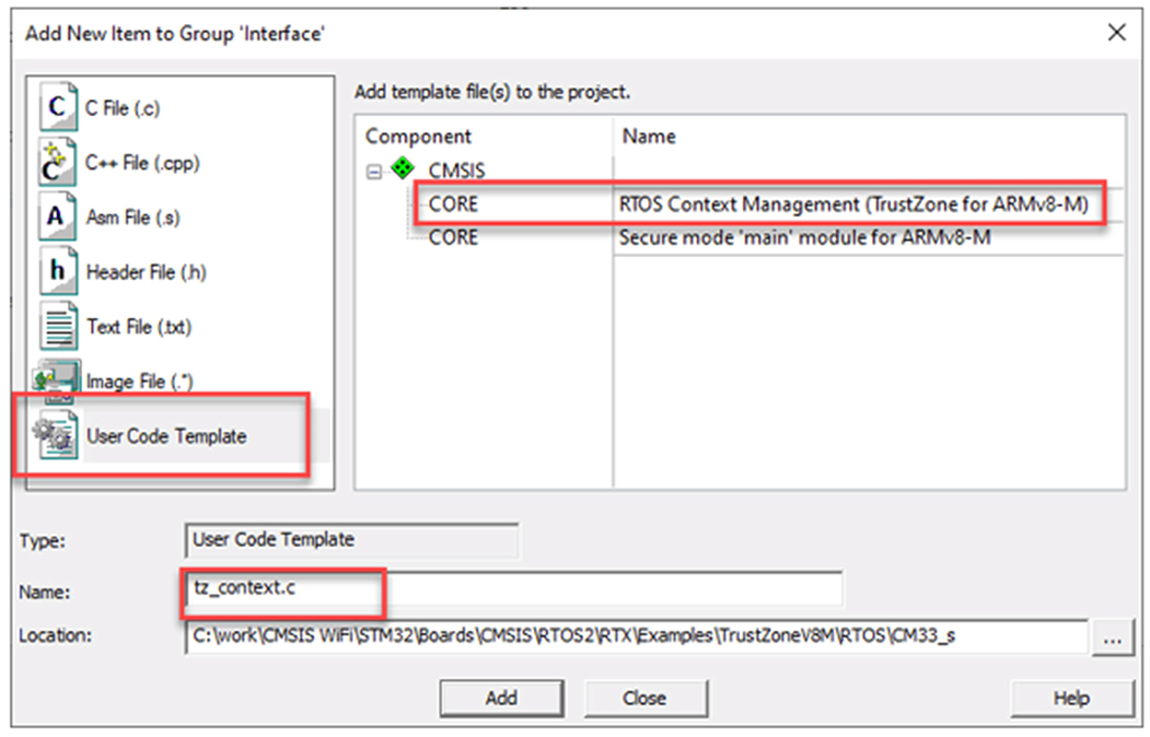
Fig. 10.42 Secure context template. Add the secure context template to the secure project. No permission required.
- Set the Nonsecure project as the active project.
- Open the RTE and select the CMSIS::RTOS2:Keil RTX5.
- Ensure the variant is set to Source:NS or Library_NS (Fig. 10.43).
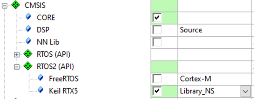
Fig. 10.43 Selecting RTOS security model. Use the RTE to add the Nonsecure version of the RTX RTOS. No permission required.
- Then click OK to close the RTE.
- Open main_ns.c in the Nonsecure project.
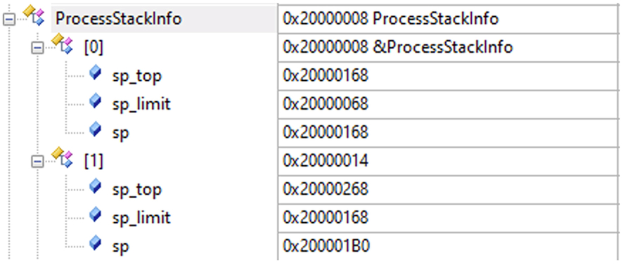
When the main() function initializes the RTOS, the kernel will call the secure TZ_InitContextSystem_S() function. This function initializes the Secure process stack pointer and subdivides the stack space into a set of slots. The number of available slots is defined at the top of the module, along with the size of each slot in bytes.
The slot details are held in an array of structures called processStackInfo. This contains the PSP value for the start of the stack, the top of the stack, and a value for the stack limit register (Fig. 10.44).
The main function can now create some threads. The first two threads, ThreadA() and ThreadB(), contain code that will access the secure functions. Both threads are created with a thread attribute as shown below:
static const osThreadAttr_t ThreadAttr = { .tz_module = 1U, // indicate calls to secure mode }; ThreadA_Id = osThreadNew(ThreadA, NULL, &ThreadAttr); ThreadB_Id = osThreadNew(ThreadB, NULL, &ThreadAttr); ThreadC_Id = osThreadNew(ThreadC, NULL, NULL);
The thread attribute sets the TrustZone module identifier to logic one, which will force the RTOS kernel to call the secure TZ_AllocModuleContext() function. This will allocate a stack slot and memory ID to this function. The final thread is created with a default thread attribute structure. Here, the TrustZone module identifier is set to zero, meaning that this thread does not access any secure functions.
Once the RTOS has started, each of the threads will task switch. During each task switch, the kernel will call the TZ_StoreContext_S() function. This function performs limit checks to ensure the current value of the stack pointer is within the active slot. If everything is OK, it stores the current value of the stack pointer in the processStackInfo array.
ProcessStackInfo[slot].sp = sp;
We then load in the new thread context with TZ_LoadContext_S(). On entry, this function checks for a valid slot number before restoring the secure process stack value and setting the stack limit register for the current slot.
- Use batch build to build both projects.
- Start the debugger.
- Breakpoints are set on each of the TrustZone context functions and also on the nonsecure thread functions.
- Open the register window so you can see the secure stack pointers.
The watch window contains the ProcessStackInfo array.
- Run the code between the breakpoints to see the TrustZone context functions manage the secure memory allocation between the Nonsecure threads.
Memory protection unit (MPU)
The Memory Protection Unit (MPU) is an optional system level peripheral that may be added to the processor when the silicon vendor designs their microcontroller. Strictly speaking, the MPU is not part of TrustZone and may be fitted in isolation. However, it is likely that if TrustZone is fitted, the MPU will also be present. The purpose of the MPU is to mark the Cortex-M33 memory map into different memory regions, which are each granted different access permissions. So, for example, we can define a region over the FLASH memory, which has execute only access, privileged access, nonprivileged. Another region can be defined over the SRAM, which has Read/Write access and no execute access. While this sounds similar to TrustZone and the SAU, the MPU is a means of further policing memory access. Another important difference is that the TrustZone Secure and Nonsecure regions are defined at startup and never changed during normal execution. Whereas the MPU regions can be changed on the fly as different code executes. In an ideal system, we can use TrustZone to partition the device memory and the MPU to sandbox the resources of each RTOS thread to achieve a high level of memory protection.
The Armv8-M architecture has a new generation of MPU, which supports 4, 8, 12, or 16 protection regions. Each region is defined by a start address and an end address and can overlay any memory area and can be any size from 32 bytes up to 4 GB. This gives us a lot more flexibility compared to the original Armv7-M MPU, which could only allocate region sizes from a range of fixed block sizes. With the Armv8-M MPU, the only limitation is that the start and end address must be aligned to a 32-byte boundary. Access to each memory region is then controlled by a set of attributes that define the access type, operating mode and TrustZone state. Once active, they will monitor each region, and any infraction of the region attributes will cause an MPU exception.
When the MPU is present in a microcontroller that has TrustZone, there are effectively two MPUs: one which is used to configure regions in the Nonsecure partition and the other which is used to define regions in the Secure partition. Both MPUs are programmed in exactly the same way through mirrored sets of registers. The MPU registers are banked, with one set appearing in the Secure partition and one set appearing in the Nonsecure partition. An application can only access the Nonsecure MPU when it is executing in the Nonsecure mode. However, code running in the Secure partition can access the Secure MPU through the standard registers and also access the Nonsecure MPU through a set of alias registers. To complicate things a little bit more, it is only possible to program either the Nonsecure or Secure MPU when the processor is running in privileged mode.
The Armv8-M MPU is designed to work with all Arm Cortex-A/ -R/ -M processors, not just Cortex-M. Consequently, it supports some hardware features that are not available within the Cortex-M family. This can make reading the datasheet confusing, particularly when it defines supported memory types. I will give a brief overview of the MPU memory options here, and then we will look at how to configure the MPU for a practical Cortex-M33 application.
MPU memory types
The MPU allows you to define two different types of memory region that describe how the processor can interact with the MCU memory. The two types of region are termed Normal and Device.
Normal memory
Normal memory allows more advanced Cortex-A processors to optimize code execution by reordering and merging memory accesses. In addition, normal memory can be made to work with any caches that are present in the MCU and the cache policy for each region is configured as part of the MPU region attributes Table 10.10. For future use, the Cortex-M33 is designed to work with multiple cache units for both internal and external memory, but at the time of writing, there are no Cortex-M33 MCU’s available with a cache.
| Attribute | Description |
|---|---|
| Cacheability | Define the Cache policy |
| Shareability | Define if the memory region can be shared with other bus masters |
| eXecute never | The memory region may be executable or Never Execute |
The MPU can define the normal memory attributes.
The cacheability field has several subfields as shown in table that allow the MPU to define the full cache policy (Table 10.11).
| Attribute | Description |
|---|---|
| Cache Policy | Write Through or Write Back |
| Allocation | Cache line allocation hints |
| Transient Hint | Hint to the cache that the data is only needed temporarily |
The MPU can control the cache policy of an internal cache.
Shareability
In a system with multiple bus masters, which may be in the form of DMA units or other processors, we can define a memory region as shareable between these different bus masters. It is also possible to create a number of separate sharable regions that are shared by different groups of bus masters. The shareability is further divided into inner and outer sharable groups.
Nonshareable
The region is only accessed by the CPU and is not accessed by any other bus masters.
Inner shareable
The inner shareable regions are associated with caches integrated within the microcontroller. In a complex memory system, the inner cache signals may be exposed to the external memory system. Multiple inner sharable regions can be defined and associated with groups of bus masters.
Outer shareable
The outer sharable regions are associated with the external memory system and allows for the implementation of an external hardware cache, which may also be shared with other system agents. The outer sharable regions can also group together inner regions so that an operation on the outer region effects all the associated inner regions.
Device memory
Device memory is used for regions that contain peripheral registers. This replaces the “Strongly Ordered” memory definition used in the earlier Armv7. MPU device memory can be used to control the type of memory access optimizations used over the MPU region (Table 10.12). With device memory, you can control if the processor can gather a number of memory accesses into a single memory transaction and whether it can reorder accesses to optimize the use of CPU registers.
| Attributes | Operand | Description |
|---|---|---|
| Gathering | G or nG | Writes to a memory region; may be merged into a single access unless they are interleaved with a memory barrier instruction |
| Reordering | R or nR | Writes to a memory region; may be reordered |
| Early Write Acknowledge | E or nE | Writes to a memory region; will use a write buffer to provide an early write acknowledge |
The device memory attributes may be combined to support four different types of memory access (Table 10.13).
| Access type | Description |
|---|---|
| nGnRnE | Strongly ordered memory that must be accessed as the code is written |
| nGnRE | Peripheral registers that may be written to without race conditions |
| nGRE | Writing to a buffer where order doesn’t matter but there is a limited access size |
| GRE | Writing to a peripheral buffer where order and access size do not matter |
MPU configuration
The MPU is configured through a set of registers that are similar in format to the SAU (Table 10.14).
| Register | Description |
|---|---|
| MPU_TYPE | Number of available MPU regions |
| MPU_CTRL | Activate the MPU regions |
| MPU_RNR | Region Number |
| MPU_RBAR | Region Base Address |
| MPU_RLAR | Region Limit Address |
| MPU_RBAR_A1—MPU_RBAR_A3 | Region Base Address Alias Registers 1–3 |
| MPU_RLAR_A1—MPU_RLAR_A3 | Region Limit Address Registers 1–3 |
| MPU_MAIR0—MPU_MAIR1 | Attribute Indirection Registers 0–1 |
The MPU_Type register contains a field called DREGION that returns the total number of MPU regions available for the current security state. If you are writing code for a specific microcontroller, you will know this from the datasheet.
The MPU_CTRL contains three bits as shown in Table 10.15.
| MPU CTRL bit | Name | Description |
|---|---|---|
| 0 | ENABLE | Enable/Disable the MPU |
| 1 | HFNMIENA | Enable for hard fault and NMI exceptions |
| 2 | PRIVDEFENA | Set privileged access for the entire memory map |
Once we have configured the required MPU regions, they will become active when the CTRL enable bit is set to logic 1. If we want to reconfigure a region, it is first necessary to disable the MPU, adjust the region then re-enable the MPU. The PRIVDEFENA bit is used to define the default global memory map. If it is set to logic 1, then the default is privileged access across the entire 4GB address space, whatever the current security state. The MPU regions are then used to create unprivileged regions for the background code. If PRIVDEFENA is set to logic zero, the processor can only access regions defined in the MPU, and a fault will be raised if the code tries to access memory outside of the defined MPU regions.
Region number register
The MPU has a small number of registers that are used to program any of the available MPU regions. When we need to configure a specific region, it is first selected by entering the desired region number into the region number register (Table 10.16). The remaining MPU region registers can then be used to configure the selected region.
Base address register
Once the region has been selected, we define its base address by programming bits 31–5 in the base address register (Table 10.17). The lower five bits of the region base address are always set to zero. However, in the actual Base Address Register, the lower five bits have a secondary function that allows us to configure the access permissions for the region. If bit zero is set to logic 1, this region will not allow code execution.
| Bit field | Name | Description |
|---|---|---|
| 0 | XN | Execute Never |
| 1–2 | AP | Access Permissions |
| 3–4 | SH | Shareable |
| 5–31 | BASE | Base Address of the region (zero extended over bits 0–4) |
Read-write access permissions can be defined with bits 2–1, as shown in Table 10.18. Here, we can allow read/write or read-only access. This can be further qualified by the operating mode of the processor (privileged or unprivileged).
| Bit field | Description |
|---|---|
| 00 | Read/Write by privileged code only |
| 01 | Read/Write by privileged and unprivileged code |
| 10 | Read only by privileged code |
| 11 | Read only by privileged and unprivileged code |
We can also define how the memory region is shared between the processor and other bus masters such as DMA units and other processors (Table 10.19). Memory used solely by the Cortex-M33 processor should be declared as nonshareable. Then, depending on how the silicon vendor has designed the MCU, there may be regions of memory shared between bus masters. These can be grouped into inner regions and outer regions. Each inner region is independently defined, but inner regions may be grouped within an outer region. Then operations on an outer region will affect all the associated inner regions.
Memory attribute indirection registers
The Memory Attribute Indirection Registers allow you to define a further “table” of memory attributes that can be used as a fast method of setting up and changing MPU regions on the fly. The two indirection registers are each divided into four attribute fields (Fig. 10.45). Each attribute field is eight bits wide and is used to hold a set of user-defined memory attributes that may be assigned to multiple MPU regions.

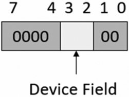
Each attribute field can be configured to support Normal or Device memory. To configure an attribute field for device memory, all bits in the field should be set to zero except bits 3–2, the device field (Fig. 10.46).
In the device field, we can define the type of access permitted to the memory region in terms of gathering, reordering, and write acknowledgement (Table 10.20).
| Bit field | Type | Description |
|---|---|---|
| 00 | Device—nGnRnE | Nongathering, nonreordering, nonearly write acknowledge |
| 01 | Device—nGnRE | Nongathering, nonreordering, early write acknowledge |
| 10 | Device—nGRE | Nongathering, reordering, early write acknowledge |
| 11 | Device—GRE | Gathering, reordering, early write acknowledge |
Generally, when defining an MPU region that will cover the MCU peripheral registers, you should declare the region as “Nongathering, Nonreordering with early write acknowledge” nGnRE.
An attribute field can be programmed to configure normal memory. In this case, the field is split into two nibbles, which are used to configure the inner and outer caches (Fig. 10.47).
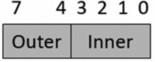
The upper nibble is then used to configure the outer cache policy while the lower nibble is used to configure the inner cache policy.
Region Limit Register.
The region limit register defines the end address of the MPU region. The upper limit address is defined in bits 31–5, and the lower 5 bits are extended using the value 0x1F.
The lower five bits within the Region Limit Register can be programmed by a user to configure the MPU region attributes. Bits 3–1 act as a pointer to the eight attribute fields defined in the memory attribute indirection registers (Fig. 10.48). This allows us to select from a group of predefined attributes.
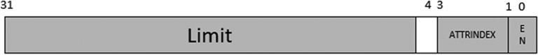
Finally, we can enable a region by setting bit zero. The MPU regions will not become active until the global enable bit is set in the MPU CTRL register.
Region Base Address Alias 1–3 and Region Limit Address Alias 1–3.
The Region Base and Limit Alias Registers provide a fast method of configuring MPU up to three additional regions without having to individually configure the Region Number Register Address and Limit Registers. Each pair of Region Alias Registers contain the same fields as the Region Base and Region Limit Address Registers. This allows us to pre-program each pair of alias registers with the configuration values for an MPU region. When the Region Number Register is updated, the alias regions will be programmed in addition to the Region Base Address and Limit Registers. The regions accessible by the alias registers is defined by bits [7:2] of the Region Number Register using the formula (RNR[7:2] < < 2 + n), where n is the number of the alias register pair (Fig. 10.49).
Exercise: Memory protection unit
This example demonstrates configuration and reconfiguration of the Secure and Nonsecure MPU during code execution.
- In the pack installer select and copy exercise 10.5.
- Set the Secure project as the active project.
- In the project window select the Secure Code Group.
- Right click and select Add existing files.
- Add the file MPU.c.
- Open MPU.c.
This file uses the CMSIS Core MPU functions to define protection regions for the Secure and Nonsecure MPU’s.
We first need to define settings for the attribute registers, this can be done directly by a CMSIS core function (Table 10.21).
| Function | Description |
|---|---|
| void ARM_MPU_SetMemAttr(uint8_t idx,uint8_t attr) | idx The attribute index to be set [0–7] attr The attribute value to be set. |
| ARM_SetMemAttr_NS(uint8_t idx,uint8_t attr) | idx The attribute index to be set [0–7] attr The attribute value to be set. |
| void ARM_MPU_SetMemAttrEx(MPU_Type * mpu,uint8_t idx,uint8_t attr) | MPU pointer to the required MPU idx The attribute index to be set [0–7] attr The attribute value to be set. |
Some additional macros are provided to define the attribute bit field (Table 10.22).
| Function | Description |
|---|---|
| ARM_MPU_ATTR(O,I) | Defines attributes as Normal or device memory |
| ARM_MPU_ATTR_MEMORY_(NT, WB, RA, WA) | Normal Memory attributes NT Nontransient: WB Write-Back RA Read Allocation WA Write Allocation |
| ARM_MPU_ATTR_DEVICE (0 U) | Device memory |
| ARM_MPU_ATTR_DEVICE_nGnRE | Nongathering, Nonreordering, No Early Write Acknowledge |
| ARM_MPU_ATTR_DEVICE_nGnRnE | Nongathering, Nonreordering, No Early Write Acknowledge |
| ARM_MPU_ATTR_DEVICE_nGRE | Nongathering, Reordering, Early Write Acknowledge |
We can use the CMSIS functions and macros to define attributes for a FLASH and RAM region.
/* Normal memory */ ARM_MPU_SetMemAttr(0UL, ARM_MPU_ATTR( /*Outer Write-Backtransient with read and write allocate*/ ARM_MPU_ATTR_MEMORY_(0UL, 1UL, 1UL, 1UL),
/*Inner Write-Throughtransient with read and write allocate*/ ARM_MPU_ATTR_MEMORY_(0UL, 0UL, 1UL, 1UL) );
Now when we define an MPU region the attributes will be referenced to define the access rights (Table 10.23).
- Open the MPU window in the peripheralscore peripherals Memory Protection Unit (Fig. 10.50).
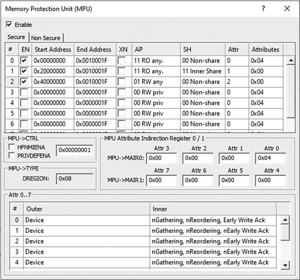
Fig. 10.50 MPU debug view. The debugger can display the current MPU settings in a peripheral window. No permission required.
- Step through the example code and observe the MPU configuration and code execution.
| Function | |
|---|---|
| void ARM_MPU_SetRegion(uint32_t rnr,uint32_t rbar,uint32_t rlar) | rnrRegion number to be configured.rbarValue for RBAR register.rlarValue for RLAR register. |
| void ARM_MPU_SetRegion_NS(uint32_t rnr,uint32_t rbar,uint32_t rlar) | rnrRegion number to be configured.rbarValue for RBAR register.rlarValue for RLAR register. |
| ARM_MPU_RBAR(BASE, SH, RO, NP, XN) | BASE The base address bits SH Shareability RORead-Only: Set to 1 for a read-only memory region. NP nonprivileged: (unprivileged) Set to 1 for a nonprivileged memory region. XN eXecute Never: Set to 1 for a nonexecutable memory region. |
| ARM_MPU_RLAR(LIMIT, IDX) | LIMIT The limit address bits IDX The attribute index to be associated with this memory region. |
CMSIS-zone
So far, we have looked at configuring the TrustZone SAU and the MPU through handwritten source code. While this is OK in a simple system, in a real project, the complexity can rise very quickly, particularly if our hardware contains multiple processors. In a real system, this makes it difficult to create and maintain an accurate set of configuration files across multiple projects. To make this process, easier CMSIS-Zone is a new standard that specifies a markup language to describe the full project memory map and how it subdivides between subprojects and execution regions within those projects. CMSIS-Zone is based on an open-source markup language called FreeMarker (Fig. 10.51).
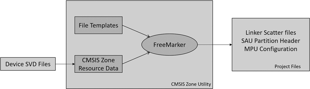
CMSIS-zone utility
CMSIS-Zone provides a plugin utility for the Eclipse IDE, which can be used to graphically define the full project resources and then subdivide and allocate them to the application projects and their execution regions. The CMSIS-Zone utility will then generate a set of C source files that configure the SAU and the MPU, plus a set of matching linker script files.
Exercise: Using the CMSIS-zone utility
In this exercise, we will use the CMSIS-Zone utility to configure Zones (projects) for the Secure and Nonsecure TrustZone partitions. The utility will then generate the necessary source, header, and project files, which can be added to our Microvision projects.
In the pack installer select and copy exercise 10.6.
The CMSIS-Zone project can use the CMSIS pack files to define the microcontroller resources or we can use an existing Resource Zone file (rzone). The example project contains a resource file and template files to generate the final zone support files
Typically, a resources file will be provided by the silicon vendor, if one is not available you can use the pack system.
To avoid having to reinstall the packs, we can use the existing microVision pack repository.
- Download an install the CMSIS-Zone utility from the link below.
- StartEclipse.
- Import the example Zone project using FileImportGeneralProjects from Folder or Archive
- In the top right hand corner select the pack installer icon (Fig. 10.52).
Fig. 10.52 Eclipse pack installer. Open the pack installer in the CMSIS-Zone Eclipse IDE. No permission required.
- This will open the pack perspective.
Rather than reinstall the Device Family Packs we can set the CMSIS-Zone utility tool to access the packs installed in the MDK-Arm repository.
- Press the “Manage Local Repositories” icon on the packs toolbar.
- Select the CMSIS Packs tab.
- Enter the path to the MDK-Arm pack folder C:Keilarmpack (Fig. 10.53).
Fig. 10.53 CMSIS pack path. Set the CMSIS-Zone pack path to import the existing Arm-MDK repository. No permission required.
- Close the menu and switch back switch back to the project perspective (Fig. 10.54).
Fig. 10.54 Eclipse project perspective. Open the Eclipse project perspective. No permission required.
- Select newprojectCMSISCMSIS-Zone Project (Fig. 10.55).
Fig. 10.55 Eclipse zone project. Create a CMSIS-zone project. No permission required.
- Click the Next button and we have a choice to use a resource file or the pack system (Fig. 10.56). Select the LPC55S69.rzone resource file in the example project.
Fig. 10.56 Resource file selection. Import the resource file to define the microcontroller memory map. No permission required.
The silicon vendor may provide a resource file that defines the FLASH, RAM, and peripherals within on their device. If this is not available, you can select the device pack, and the CMSIS-Zone utility will create a resource file from the pack description files. This route may require you to add and check definitions, so a resource file is the best route.
- Select the Resources tab to display the microcontroller memory and peripheral resources (Fig. 10.57).
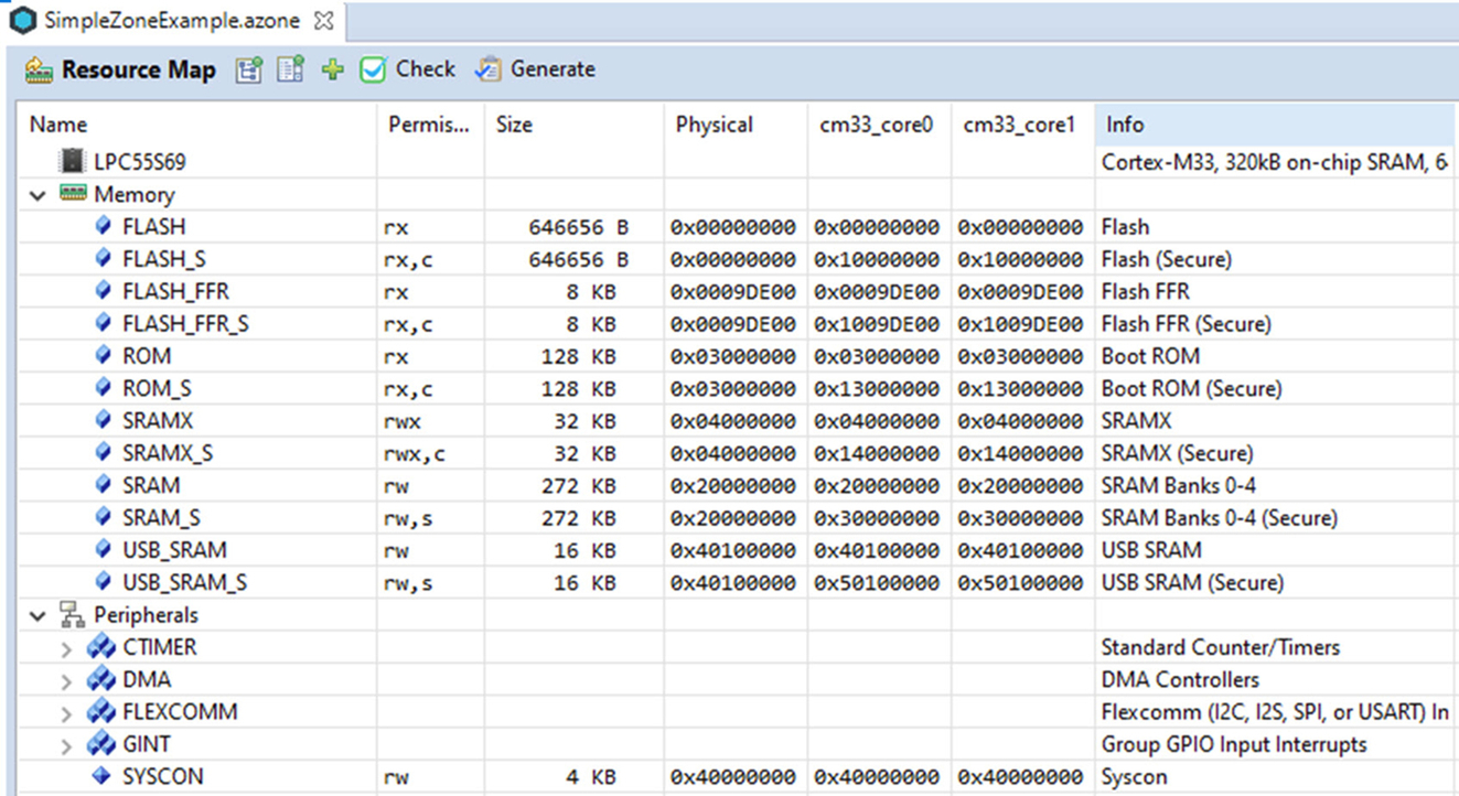
Fig. 10.57 Zone memory map. Once the project has been created the microcontroller memory map is displayed. No permission required.
Creating a zone project is a two-step process. First, we must define which resources belong to the Secure and Nonsecure world. This means subdividing the physical memory into subregions within the Secure and Nonsecure alias regions. The second stage is to allocate the memory subregions as resources to separate zones where a zone corresponds to a Microvision project (Fig. 10.58).
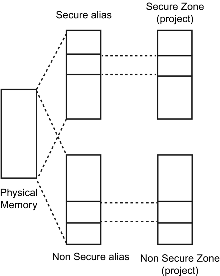
First we need to create memory regions for the Secure and Nonsecure projects by defining subregions within each block of memory.
- Select the secure flash (FLASH_S) right click and select add memory region (Fig. 10.59).
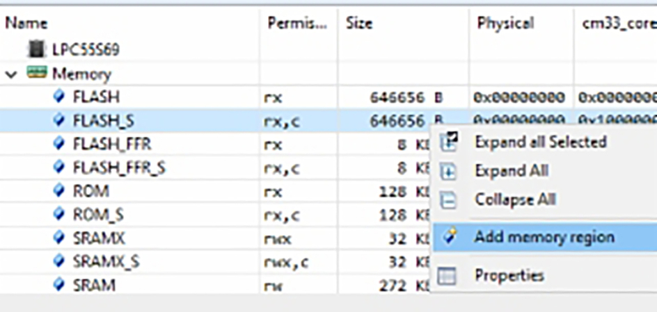
Fig. 10.59 Allocate resources to project zones. The default memory map can be subdivided into memory regions, which can be allocated to zone projects. No permission required.
- Name the region as Startup, set the size to 10 K and select its security type as Secure (Fig. 10.60).
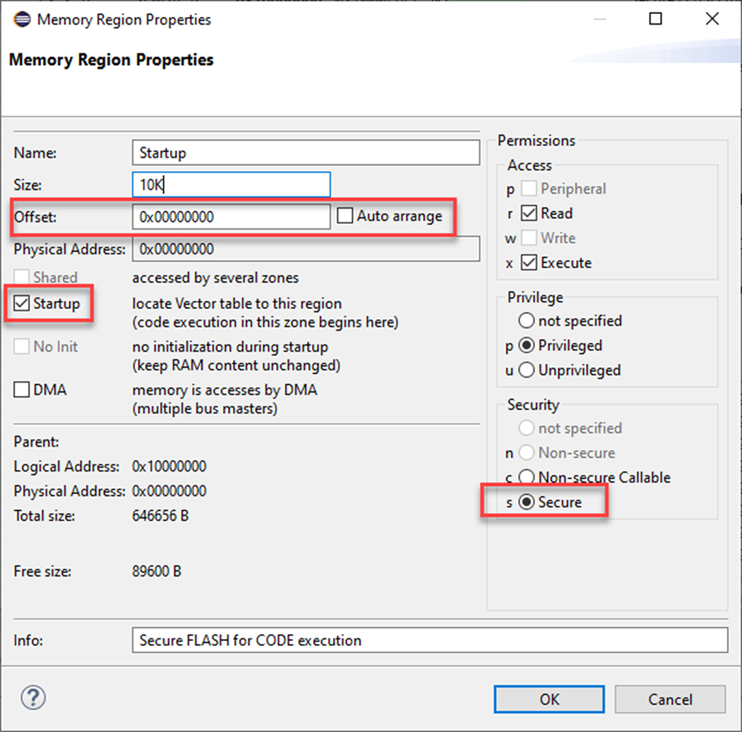
Fig. 10.60 Memory region configuration options. We can configure the memory region options in its local dialogue. No permission required.
The memory region dialogue allows us to configure the size location and access properties for our new segment.
- Define the following memory regions (Table 10.24).
Zone utility regions. Parent region Sub region name Size Offset Security Additional FLASH_S TF_M Startup 10 K 0 × 00000000 Secure Startup FLASH_S VENEER 4 K Nonsecure callable FLASH_S TF-M 128 K Auto Secure FLASH Application_NS 128 K 0 × 30000 Nonsecure SRAM_S Secure_RAM 128 K Auto Default Secure SRAM Application_RAM_NS 128 K Auto Nonsecure DMA Project zone memory regions.
By default the each of the microcontroller peripherals interrupt lines will be routed to the secure NVIC.
We can change this by explicitly defining a peripheral as Nonsecure.
- Select CTIMER0.
- Right click and select Properties (Fig. 10.61).
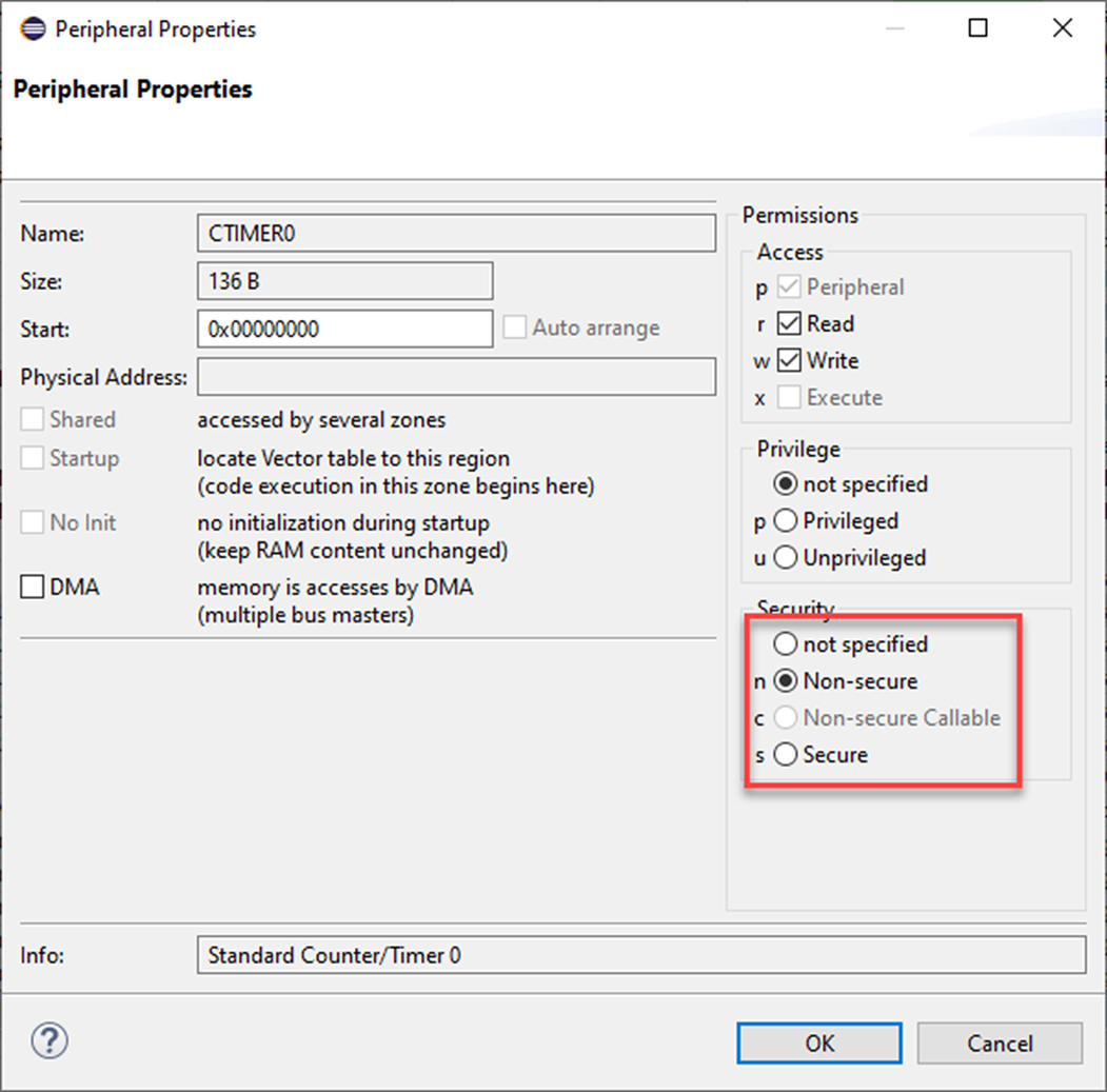
Fig. 10.61 Peripheral configuration options. Each peripheral can be marked for either security world. No permission required.
- Within the Properties menu set the security type to Nonsecure.
This creates the memory map regions that we are going to need for our projects. The next step is to create the project Zones and allocate resources to each project.
- Select the Zones tab (Fig. 10.62).
Fig. 10.62 Zone selection tab. Select the zone tab at the bottom of the screen. No permission required.
- On the zone map tool bar press the green cross (light gray in print version) to create a new zone (Fig. 10.63).
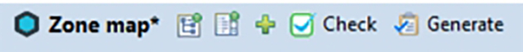
Fig. 10.63 CMSIS zone utility toolbar. Now create a new Zone (project) using the green cross icon (light gray in print version) on the toolbar. No permission required.
- Call this zone secure_world and set the security type to Secure (Fig. 10.64).
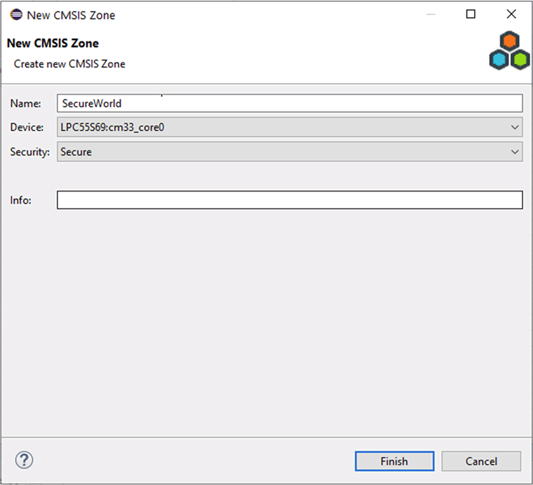
Fig. 10.64 New CMSIS zone dialogue. As a new CMSIS zone is created, we can define its name and security world. No permission required.
Create a second zone called non_secure_world and set its security type to Nonsecure.
This now creates an additional selection column for each zone (Fig. 10.65).
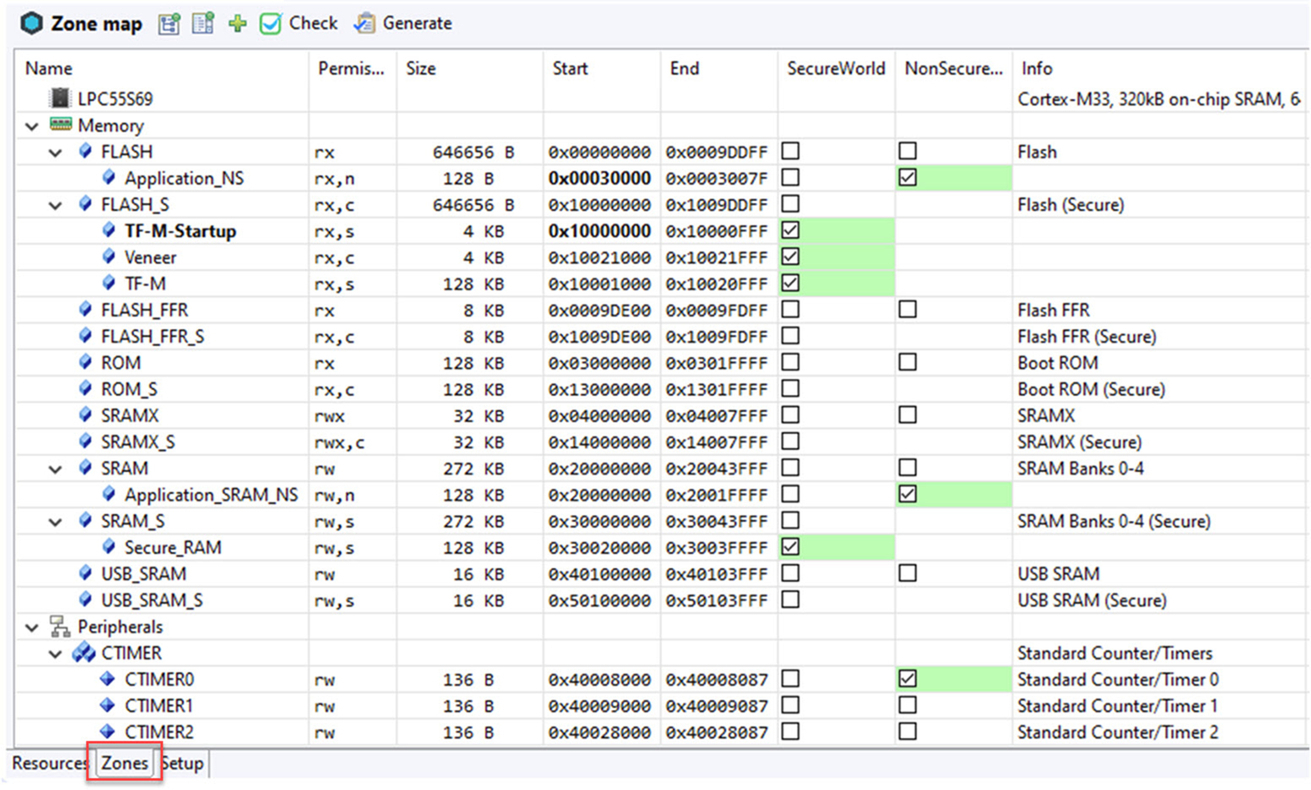
Each column will contain selection boxes for memory regions associated with its security type.
We can now allocate resources to the Secure and Nonsecure zones. This will allow CMSIS Zone to generate the support files from a set of generic template files which must be located in the projects FTL directory
- Before we can generate the zone support files you must copy the contents of the example FTL directory to your projects FTL directory.
Once you have allocated the memory resources press the generate button on the toolbar.
This will create the memory map header file, SAU and MPU configuration code and the matching linker scatter files.
Code is also produced for some additional device-specific bus filters called the Memory Protection Controller and Peripheral Protection Controller, which we will see in the next chapter.
- Once the files are generated open the zone project directory and copy the files to the example project directory.
- Start microVision and build the example project using the CMSIS-Zone files.
You should now be able to start the debugger and use the peripheralcore peripheral windows to examine how the processor TrustZone and MPU registers are configured.
Conclusion
As well as providing code to configure the Cortex-M33 TrustZone regions, some additional functions configure additional security peripherals called the Memory Protection Controller (MPC) and Peripheral Protection Controller (PPC). These are additional bus filtering gateways that are used to extend the memory partition definitions to a wider system that contains further bus Masters (additional processors, DMA units). The MPC and PPC are used to fully enforce the security memory map to create a Trusted Execution Environment. In the next chapter, we will see how TrustZone is integrated into a standard microcontroller.