
CHAPTER 11
Differential Pairs and Differential Impedance
A differential pair is simply a pair of transmission lines with some coupling between them. The value of using a pair of transmission lines is not so much to take advantage of the special properties of a differential pair as to take advantage of the special properties of differential signaling, which uses differential pairs.
Differential signaling is the use of two output drivers to drive two independent transmission lines, one line carrying one bit and the other line carrying its complement. The signal that is measured is the difference between the two lines. This difference signal carries the information.
Differential signaling has a number of advantages over single-ended signaling, such as the following:
• The total dI/dt from the output drivers is greatly reduced over single-ended drivers, so there is less ground bounce, less rail collapse, and potentially less EMI.
• The differential amplifier at the receiver can have higher gain than a single-ended amplifier.
• The propagation of a differential signal over a tightly coupled differential pair is more robust to cross talk and discontinuities in the return path shared by the two transmission lines in the pair.
• Propagating differential signals through a connector or package will be less susceptible to ground bounce and switching noise.
• A low-cost, twisted-pair cable can be used to transmit a differential signal over long distances.
The most important downside to differential signals comes from the potential to create EMI. If differential signals are not properly balanced or filtered, and there is any common signal component present, it is possible for real-world differential signals that are driven on external twisted-pair cables to cause EMI problems.
The second downside is that transmitting a differential signal requires twice the number of signal lines as transmitting a single-ended signal. The third downside is that there are many new principles and a few key design guidelines to understand about differential pairs. Due to the non-intuitive effects in differential pairs, there are many myths in the industry that have needlessly complicated and confused their design.
Ten years ago, less than 50% of the circuit boards fabricated had controlled-impedance interconnects. Now, more than 90% of them have controlled-impedance interconnects. Today, less than 50% of the boards fabricated have differential pairs. In a few years, we may see over 90% with differential pairs.
11.1 Differential Signaling
Differential signals are widely used in the small computer system interface (SCSI) bus; in Ethernet; in USB; in many of the telecommunications optical-carrier (OC) protocols, such as OC-48, OC-192, and OC-768; and for all high-speed serial protocols. One of the popular signaling schemes is low-voltage differential signals (LVDS).
When we look at a signal voltage, it is important to keep track of where we are measuring the voltage. When a driver drives a signal on a transmission line, there is a signal voltage on the line that is measured between the signal conductor and the return path conductor. We usually refer to this as the single-ended transmission-line signal. When two drivers drive a differential pair, in addition to the two single-ended signals, there is also a voltage difference between the two signal lines. This is the difference voltage, or the differential signal. Figure 11-1 illustrates how these two different signals are measured in a differential pair.
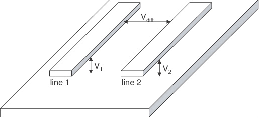
Figure 11-1 The single-ended signal is measured between the signal conductor and the return conductor. The differential signal is measured between the two signal lines in a differential pair.
In LVDS, two output pins are used to drive a single bit of information. Each signal has a voltage swing from 1.125 v to 1.375 v. Each of these signals drives a separate transmission line. The single-ended voltage between the signal and return paths of each line is shown in Figure 11-2.

At the receiver end, the voltage on line 1, measured between the signal line and its return path, is V1 and the voltage on line 2 is V2. A differential receiver measures the differential voltage between the two lines and recovers the differential signal:
where:
Vdiff = differential signal
V1 = signal on line 1 with respect to its return path
V2 = signal on line 2 with respect to its return path
In addition to the intentional differential signal that carries information, there may be some common signal. The common signal is the average voltage that appears on both lines, defined as:
where:
Vcomm = common signal
V1 = signal on line 1 with respect to its return path
V2 = signal on line 2 with respect to its return path
TIP
These definitions of differential and common signals apply universally to all signals. When any arbitrary signal is generated on a pair of transmission lines, it can always be completely and uniquely described by a combination of a common- and a differential-signal component.
Given the common and differential signals, the single-ended voltages on each line with respect to the return plane can also be recovered from:
where:
Vcomm = common signal
Vdiff = differential signal
V1 = signal on line 1 with respect to its return path
V2 = signal on line 2 with respect to its return path
In LVDS, there are some differential-signal components and some common-signal components. These signal components are displayed in Figure 11-3. The differential signal swings from −0.25 v to +0.25 v. As the differential-signal propagates down the transmission line, its voltage is a 0.5-v transition. When describing the magnitude of the differential signal, we usually refer to the peak-to-peak value.
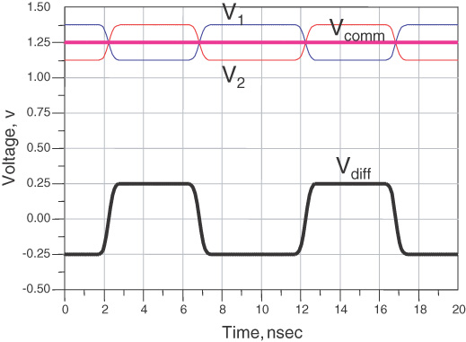
Figure 11-3 The common- and differential-signal components in LVDS. Note that there is a very large common-signal component, which, in principle, is constant.
There is also a common signal. The average value is 1.25 v. This is more than a factor of 2 larger than the differential-signal component.
TIP
Even though an LVDS is called a differential signal, it has a very large common-signal component, which is nominally constant.
When we call an LVDS a differential signal, we are really lying. It has a differential component, but it also has a very large common component. It is not a pure differential signal. In ideal conditions, the common signal is constant. The common signal normally will not have any information content and will not affect signal integrity or system performance.
Unfortunately, as we will see, very small perturbations in the physical design of the interconnects can cause the common-signal component to change, and a changing common-signal component has the potential of causing two very important problems:
1. If the value of the common signal gets too high, it may saturate the input amplifier of the differential receiver and prevent it from accurately reading the differential signal.
2. If any of the changing common signal makes it out on a twisted-pair cable, it has the potential of causing excessive EMI.
The terms differential and common always and only refer to the properties of the signal, never to the properties of the differential pair of transmission lines themselves. Misuse of these terms is one of the major causes of confusion in the industry.
11.2 A Differential Pair
All it takes to make up a differential pair is two transmission lines. Each of the two transmission lines can be a simple, single-ended transmission line. Together, the two lines are called a differential pair. In principle, any two transmission lines can make up a differential pair.
Just as there are many cross sections for a single-ended transmission line, there are many cross sections for differential pair transmission lines. Figure 11-4 shows the cross sections of the most popular geometries.

Although, in principle, any two transmission lines can make up a differential pair, five features will optimize their performance for transporting high-bandwidth difference signals:
1. The most important property of a differential pair is that it be of uniform cross section down its length and provide a constant impedance for the difference signal. This will ensure minimal reflections and distortions for the differential signal.
2. The second most important property is that the time delay between each line is matched so that the edge of the difference signal is sharp and well defined. Any time delay difference between the two lines, or skew between them, will also cause a distortion of the differential signal and some of the differential signal to be converted into common signal.
3. Both transmission lines should look exactly the same. The line width and dielectric spacing of the two lines should be the same. This property is called symmetry between the two lines. There should be no other asymmetries such as a test pad on one and not on the other or a neck-down on one but not the other. Any asymmetries will convert differential signals into common signals.
4. Each line in a pair should have the same length. The total length of each line should be exactly the same. This will help maintain the same delay and minimize skew.
5. There does not have to be any coupling between the two lines, but most of the noise immunity benefits of differential pairs is lost if there is no coupling. Coupling between the two signal lines will allow differential pairs to be more robust to ground bounce noise picked up from other active nets than single-ended transmission lines. The greater the coupling, the more robust the differential signals will be to discontinuities and imperfections.
Figure 11-5 shows an example of a differential pair of transmission lines with a differential signal propagating. In this example, the signal on one line is a transition from 0 v to 1 v, and the other signal is a transition from 1 v to 0 v. As the signals propagate down the transmission lines, they have the voltage distribution shown in the figure.

Figure 11-5 A differential pair with a signal propagating on each line and the differential signal between the two lines.
Of course, even though we called this a differential signal, we see right away that we are lying again. It is not a pure differential signal but contains a large common signal component of 0.5 v. However, this common signal is constant, and we will ignore it, paying attention only to the differential component.
Given these voltages on each transmission line, the difference voltage can be easily calculated. By definition, it is V1 − V2. The pure differential-signal component that is propagating down the differential pair is also shown in the figure. With a 0-v to 1-v signal transition on each single-ended transmission line, the differential-signal swing is a 2-v transition propagating down the interconnect. At the same time, there is a common-signal component, 1/2 × (V1 + V2) = 0.5 v, which is constant along the line.
TIP
The most important electrical property of a differential pair is the impedance the differential signal sees, which we call the differential impedance.
11.3 Differential Impedance with No Coupling
The impedance the differential signal sees, the differential impedance, is the ratio of the voltage of the signal to the current of the signal. This definition is the basis of calculating differential impedance. What makes it subtle is identifying the voltage of the signal and the current of the signal.
The simplest case to analyze is when there is no coupling between the two lines that make up the differential pair. We will look at this case, determine the differential impedance of the pair, and then turn on coupling and look at how the coupling changes the differential impedance.
To minimize the coupling, assume that the two transmission lines are far enough apart, i.e., at least a spacing equal to twice the line width, so they do not appreciably interact with each other and so each line has a single-ended characteristic impedance, Z0, of 50 Ohms. The current going into one signal trace and out the return is:
where:
Ione = current into one signal line and out its return
Vone = voltage between the signal line and the adjacent return path of one line
Z0 = single-ended characteristic impedance of the signal line
For example, when a signal of 0 v to 1 v is imposed on one line and at the same time a 1-v to 0-v signal is imposed on the other line, there will also be a current loop into each line. Into the first line will be a current of I = 1 v/50 Ohms = 20 mA flowing from the signal conductor down to and out its adjacent return path. Into the second line will also be a current loop of 20 mA, but flowing from the return conductor up to and out its signal conductor.
The differential-signal transition propagating down the line is the differential signal between the two signal-line conductors. This differential-signal swing is twice the voltage on either line: 2 × Vone. In this case, it is a 2-volt transition that propagates down the signal-line pair. At the same time, just looking at the signal-line conductors, it looks like there is a current loop of 20 mA going into one signal conductor and coming out the other signal conductor.
By the definition of impedance, the impedance the differential signal sees is:
where:
Zdiff = impedance the differential signal sees, the differential impedance
Vdiff = difference or differential-signal transition
Ione = current into one signal line and out its return
Vone = voltage between the signal line and the adjacent return path of one line
Z0 = single-ended characteristic impedance of the signal line
The differential impedance is twice the single-ended characteristic impedance of either line. This is reasonable because the voltage across the two lines is twice the voltage across either one and its return path, but the current going into one signal and out the other is the same. If the single-ended impedance of either line is 50 Ohms, the differential impedance of the pair would be 2 × 50 Ohms = 100 Ohms.
If a differential signal propagates down a differential pair and reaches the end, where the receiver is, the impedance the differential signal sees at the end will be very high, and the differential signal will reflect back to the source. These multiple reflections will cause signal-quality noise problems. Figure 11-6 is an example of the simulated differential signal at the end of a differential pair. The ringing is due to the multiple bounces of the differential signal between the low impedance of the driver and the high impedance of the end of the line.

Figure 11-6 Differential circuit and the received signal at the far end of the differential pair when the interconnect is not terminated. There is no coupling in this differential pair. Simulated with Agilent ADS.
One way of managing the reflections is to add a terminating resistor across the ends of the two signal lines that matches the impedance the difference signal sees. The resistor should have a value of Rterm = Zdiff = 2 × Z0. When the differential signal encounters the terminating resistor at the end of the line, it will see the same impedance as in the differential pair, and there will be no reflection. Figure 11-7 shows the simulated received differential signal with a 100-Ohm differential-terminating resistor between the two signal lines.

Figure 11-7 Received differential signal at the far end of the differential pair when the interconnect is terminated. There is no coupling in this differential pair. Simulated with Agilent ADS.
Differential impedance can also be thought of as the equivalent impedance of the two single-ended lines in series. This is illustrated in Figure 11-8. Looking into the front of each line, each driver sees the instantaneous impedance as the characteristic impedance of the line, Z0. The instantaneous impedance between the two signal lines is the series combination of the impedances of each line to the return path. The equivalent impedance of the two signal lines, or the differential impedance, is the series combination:
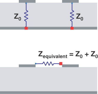
Figure 11-8 The impedance between each line and its return path in a differential pair and the equivalent impedance between the two signal lines.
Zdiff = equivalent impedance between the signal lines, or the differential impedance
Z0 = impedance of each line to the return path
If all we had to worry about was the differential impedance of uncoupled transmission lines, we would essentially be done. The differential impedance of a differential pair is always two times the single-ended impedance of either line, as seen by either driver. Two important factors complicate the real world. First is the impact from coupling between the two lines, and second is the role of the common signal and its generation and control.
11.4 The Impact from Coupling
If we bring two stripline traces closer and closer together, their fringe electric and magnetic fields will overlap, and the coupling between them will increase. Coupling is described by the mutual capacitance per length, C12, and mutual inductance per length, L12. (Unless otherwise noted, the capacitance-matrix elements always refer to the SPICE capacitance-matrix elements, not the Maxwell capacitance-matrix elements. These terms were introduced in Chapter 10, “Cross Talk in Transmission Lines.”)
As the traces are brought together, both C11 and C12 will change. C11 will decrease as some of the fringe fields between signal line 1 and its return path are intercepted by the adjacent trace, and C12 will increase. However, the loaded capacitance, CL = C11 + C12, will not change very much. Figure 11-9 shows the equivalent capacitance circuit of two stripline traces and how C11, C12, and CL vary for the specific case of two 50-Ohm stripline traces in FR4 with 5-mil-wide traces.

Figure 11-9 Variation in the loaded capacitance per length, CL, and the SPICE diagonal capacitance per length, C11. Also plotted is the variation in the coupling capacitance, C12. Simulated with Ansoft’s SI2D.
TIP
It is important to note that the coupling described by the capacitance- and inductance-matrix elements is completely independent of any applied voltages. It is purely related to the geometry and material properties of the collection of conductors.
Both L11 and L12 will change as the traces are brought together. L11 will decrease very slightly (less than 1% at the closest spacing) due to induced eddy currents in the adjacent trace, and L12 will increase. This is shown in Figure 11-10.
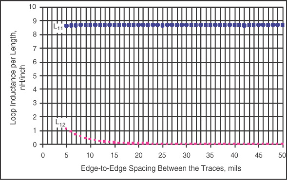
Figure 11-10 Variation in the loop self-inductance per length, L11, and the loop mutual inductance per length, L12. Simulated with Ansoft’s SI2D.
As the two traces are brought together, the coupling increases. However, even in the tightest spacing, the spacing equal to the line width, the maximum relative coupling, C12/CL or L12/L11, is less than 15%. When the spacing is more than 15 mils, or three times the line width, the relative coupling is reduced to 1%—a negligible amount. Figure 11-11 shows how this ratio, both the relative capacitive coupling and the relative inductive coupling, changes as the separation changes.

Figure 11-11 Relative mutual capacitance and mutual inductance as the spacing between two 50-Ohm, 5-mil stripline traces in FR4 changes. The relative coupling capacitance and coupling inductance are identical for a homogeneous dielectric structure such as stripline. Simulated with Ansoft’s SI2D.
When the lines are far apart, the characteristic impedance of line 1 is completely independent of the other line. The characteristic impedance varies inversely with C11:
where:
Z0 = characteristic impedance of the line
C11 = capacitance between the signal trace and the return path
When the lines are brought closer together, the presence of the other line will affect the impedance of line 1. This is called the proximity effect. If the second line is tied to the return path—i.e., a 0-v signal is applied to line 2, and only line 1 is being driven—the impedance of line 1 will depend on its loaded capacitance in the proximity of the other line. The characteristic impedance of the driven line will be related to the capacitance per length that is being driven:
Z0 = characteristic impedance of the line
C11 = capacitance per length between the signal trace and the return path
C12 = capacitance per length between the two adjacent signal traces
CL = loaded capacitance per length of one line
As the traces move closer together, the single-ended impedance of line 1 will decrease—but only very slightly (less than 1%). Figure 11-12 shows the change in the single-ended characteristic impedance of line 1 as the two traces are brought into proximity. The single-ended characteristic impedance is essentially unchanged if the second line is pegged low and the two traces are brought closer together.

Figure 11-12 Single-ended characteristic impedance of one line when the second is shorted to the return path and the separation changes, for 5-mil-wide, 50-Ohm striplines in FR4. The small fluctuations, on the order of 0.05 Ohm, are due to the numerical noise of the simulation tool. Simulated with Ansoft’s SI2D.
However, suppose the second trace is also being driven, and the signal on line 2 is the opposite of the signal on line 1. As the signal on line 1 increases from 0 v to 1 v, the signal on line 2 is simultaneously dropped from 0 v to −1 v. As the driver on line 1 turns on, it will drive a current through the C11 capacitance due to the dV11/dt between line 1 and the return path. In addition, there will be a current from line 1 to line 2, due to the changing voltage between them, dV12/dt. This voltage will be twice the voltage change between line 1 and its return, V12 = 2 × V11.
The current into one signal line will be related to:

where:
Ione = current going into one line
v = speed of the signal moving down the signal line
C11 = capacitance between the signal line and its return path per length
V11 = voltage between the signal line and the return path
C12 = capacitance between each signal line per length
V12 = voltage between each signal line
Vone = voltage change between the signal line and return path of one line
RT = rise time of the transition
As the two traces move together and they are both being driven by signals transitioning in opposite directions, the current from the driver into line 1 and out the return path will increase in order to drive the higher capacitance of the single-ended line.
TIP
If the current increases for the same applied voltage, the input impedance the driver sees will decrease. The characteristic impedance of the line will drop if the second line is driven with the opposite signal.
Suppose the second line is driven with exactly the same signal as the first line. The driver to line 1 will see less capacitance to drive since there will be no voltage between the two signal lines and the driver will see only the C11 capacitance. When the second line is driven with the same voltage as line 1, the current into signal line 1 will be:

where:
Ione = current going into one line
v = speed of the signal moving down the signal line
C11 = capacitance between the signal line and its return path per length
V11 = voltage between the signal line and the return path
C12 = capacitance between each signal line per length
Vone = voltage change between the signal line and return path of one line
RT = rise time of the transition
We see that the characteristic impedance of one line, when in the proximity of a second line, is not a unique value. It depends on how the other line is being driven. If the second line is pegged low, the impedance will be close to the uncoupled single-ended impedance. If the second line is switching opposite the first line, the impedance of the first line will be lower. If the second line is switching exactly the same as the first line, the impedance of the first line will be higher. Figure 11-13 shows how the characteristic impedance of the first line varies as the separation changes for these three cases.
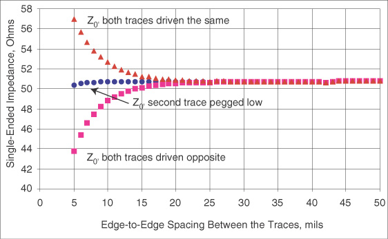
Figure 11-13 The characteristic impedance of line 1 when the second line is pegged low, switching opposite and switching the same, as the separation between the traces changes, for 5-mil-wide, 50-Ohm striplines in FR4. Simulated with Ansoft’s SI2D.
This is a critically important observation. When we only dealt with single-ended signals, a transmission line had only one impedance that described it. But when it is part of a pair and coupling plays a role, it now has three different impedances that describe it. We need to identify new labels to describe which of the three different impedances we talk about when referring to “the impedance” of a transmission line when it is part of a pair. We will therefore introduce the terms odd and even mode impedance later in this chapter to provide clear and unambiguous language describing the properties of differential pairs.
When trace separations are closer than about three line widths, the presence of the adjacent trace will affect the characteristic impedance of the first trace. Its proximity as well as the manner in which it is being driven must be considered.
The differential signal drives opposite signals on each of the two lines. As we saw above, the impedance of each line, when the pair is driven by a differential signal, will be reduced due to the coupling between the two lines.
When a differential signal travels down a differential pair, the impedance the differential signal sees will be the series combination of the impedance of each line to its respective return path. The differential impedance, with coupling, will still be twice the characteristic impedance of either line. It’s just that the characteristic impedance of each line decreased due to coupling.
Figure 11-14 shows the differential impedance as the spacing between the lines decreases. At the closest spacing that can be realistically manufactured (i.e., a spacing equal to the line width), the differential impedance of a pair of coupled stripline traces is reduced only about 12% from when the striplines are three line widths apart and uncoupled.

Figure 11-14 The differential impedance of a pair of 5-mil-wide, 50-Ohm stripline traces in FR4, as the spacing between them decreases. Simulated with Ansoft’s SI2D.
11.5 Calculating Differential Impedance
Additional formalism must be introduced to describe the impact from coupling on differential impedance, which is an effect of 12% at most. The complexity arises when quantifying the decrease in differential impedance as the traces are brought closer together and coupling begins to play a role. There are five different approaches to this analysis:
1. Use the direct results from an approximation.
2. Use the direct results from a field solver.
3. Use an analysis based on modes.
4. Use an analysis based on the capacitance and inductance matrix.
5. Use an analysis based on the characteristic impedance matrix.
There is only one reasonably close approximation useful for calculating the differential impedance of either an edge-coupled microstrip or an edge-coupled stripline, originally offered in a National Semiconductor application note by James Mears (AN-905). These approximations are based on empirical fitting of measured data.
For edge-coupled microstrip using FR4 material, the differential impedance is approximately:

where:
Zdiff = differential impedance, in Ohms
Z0 = uncoupled single-ended characteristic impedance for the line geometry
s = edge-to-edge separation between the traces, in mils
h = dielectric thickness between the signal trace and the return plane
For an edge-coupled stripline with FR4, the differential impedance is:

where:
Zdiff = differential impedance, in Ohms
Z0 = uncoupled single-ended characteristic impedance for the line geometry
s = edge-to-edge separation between the traces, in mils
b = total dielectric thickness between the planes
We can evaluate how accurate these approximations are by comparing them to the predicted differential impedance calculated with an accurate field solver. In Figure 11-15, we compare these approximations to three different cross sections for edge-coupled microstrip and edge-coupled stripline. In each case, we use the field-solver-calculated single-ended characteristic impedance in the approximation, and the approximation predicts the slight perturbation on the differential impedance from the coupling. The accuracy varies from 1% to 10%, provided that we have an accurate starting value for the characteristic impedance.
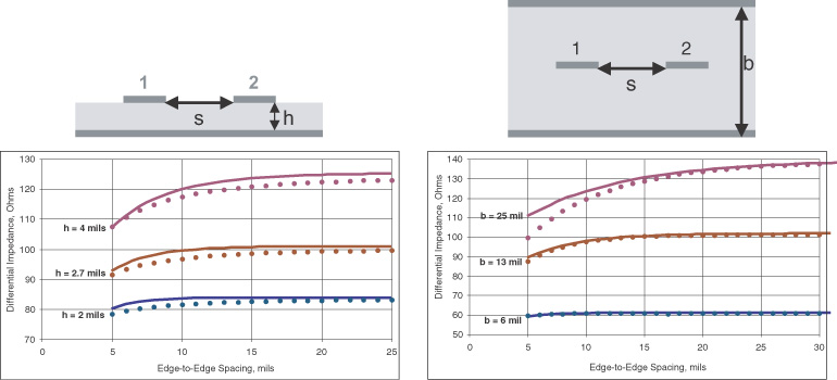
Figure 11-15 Comparing the accuracy of the differential impedance approximation with the results from a 2D field solver. In each case, the line width is 5 mils, and the material is FR4. The lines are the approximations, and the points are the simulation using Ansoft’s SI2D.
A more accurate tool that will also predict the single-ended characteristic impedance of either line is a 2D field solver. A 2D field solver requires input regarding the cross-sectional geometry and material properties. It offers output including, among other quantities, the differential impedance of the pair of lines.
The advantage of using a field solver is that some tools can be accurate to better than 1% across a wide range of geometrical conditions. They account for the first-order effects, such as line width, dielectric thickness, and spacing, as well as second-order effects, such as trace thickness, trace shape, and inhomogeneous dielectric distributions.
When accuracy is important, such as in signing off on a drawing for the fabrication of a circuit board, the only tool that should be used is a verified 2D field solver. Approximations should never be used to sign off on a design.
However, if we are limited to using only a field solver to calculate differential impedance, we will lack the terms needed to describe the behavior of common signals, terminations, and cross talk. The following sections introduces the concepts of odd and even modes and how they relate to differential and common impedance. From this foundation, we will evaluate termination strategies for differential and common signals.
We will end up introducing the description of two coupled transmission lines in terms of the capacitance and inductance matrix and the characteristic impedance matrix to calculate the odd and even mode impedances and the differential and common impedances. This is the most fundamental description and can be generalized to n different coupled lines. Ultimately, this is what is really going on inside most field solver and simulation tools.
Even without invoking more complex descriptions at this point, we have the terminology to be able to use the results from a field solver to design for a target differential impedance and evaluate another important quality of differential pairs—the current distribution.
11.6 The Return-Current Distribution in a Differential Pair
When the spacing between two edge-coupled microstrip transmission lines is greater than three times their line width, the coupling between the signal lines will be small. In this situation, as we might expect, when we drive them with a differential signal, there is some current into each signal line and an equal amount of current in the opposite direction in the return plane. An example of the current distribution for a 100-MHz differential signal into microstrip conductors that are 1.4 mils thick, or for 1-ounce copper, is illustrated in Figure 11-16.

Figure 11-16 The current distribution, at 100 MHz, in a pair of coupled 50-Ohm microstrip transmission lines, 5 mils wide and separated by 15 mils. Lighter shading means higher current density. The current density scale in the plane is 10 times more sensitive than the traces to show the current distribution more clearly. Simulated with Ansoft’s SI2D.
The direction of the current into line 1 is into the paper. The return current in the return plane below line 1 is out of the paper. Likewise, at the same time, the current into line 2 is out of the paper, and the current into its return path is into the paper. In the return plane, the return-current distributions are localized under the signal lines. When driven by a differential signal, there is virtually no overlap between the two return-current distributions in the plane.
If we pay attention only to the current in the signal traces, it looks like the same current goes into one trace and comes out the other. We might conclude that the return current of the differential signal in one trace is carried by the second trace. While it is perfectly true that the same amount of current going into one signal trace comes out of the other signal trace, it is not the complete story.
Because of the wide spacing between the differential pairs, there is no overlap of the return currents in the planes when the pair is driven with a differential signal. While it is true the net current into the plane is zero, there is still a well-defined, localized current distribution in the plane under each signal path. Anything that will distort or change this current distribution will change the differential impedance of the pair of traces.
After all, the presence of the plane defines the single-ended impedance of either trace. Increase the plane spacing, and the single-ended impedance of the trace increases, which will change the differential impedance.
Even in the extreme case for edge-coupled microstrip, bringing the signal traces as close together as is practical with a spacing equal to the line width, the degree of overlap of the currents in the return plane is very slight. The comparison of the current distributions is shown in Figure 11-17.

Figure 11-17 The current distribution, at 100 MHz, in a pair of coupled 50-Ohm microstrip transmission lines, 5 mils wide and separated by 5 mils compared with a separation of 15 mils. Lighter shading means higher current density. The current density scale in the planes is 10 times more sensitive than the traces to show the current distribution more clearly. Simulated with Ansoft’s SI2D.
TIP
When the coupling between the signal line and the return plane is much stronger than the coupling between adjacent signal traces in a differential pair, there are separate and distinct return currents in the planes and very little overlap in the return-current distributions. These current distributions will strongly affect the differential impedance of the pair. Disturb the current distribution, and the differential impedance will be affected.
For any pair of single-ended transmission lines sharing a common return conductor, if the return conductor is moved far enough away, the signals’ return-current distributions in the return conductor will completely overlap and cancel each other out, and the presence of the return conductor will play no role in establishing the differential impedance. In this specific situation, it is absolutely true that the return current of one line would be carried by the other line.
There are three such cases that should be noted:
1. Edge-coupled microstrip with return plane far away
2. Twisted-pair cable
3. Broadside-coupled stripline with return planes far away
In edge-coupled microstrip, the coupling between the two signal traces is largest when the spacing between the signal lines is as close as can be fabricated, typically equal to the line width. For the case of near-50-Ohm lines and closest spacing, as shown in Figure 11-17, there is significant return-current distribution in the return plane, and the presence of the plane affects the differential impedance. If the plane is moved farther away, the single-ended impedance of either line will increase, and the differential impedance will increase. However, as the plane is moved farther away, the return currents of the differential signal, in the plane, will increasingly overlap.
There is a point where the return currents overlap so much that there is no current in the plane, and the plane will not influence the differential impedance. This is illustrated in Figure 11-18. The single-ended impedance continues to get larger, but the differential impedance reaches a highest value of about 140 Ohms and then stops increasing. This is when the return currents completely overlap, at a trace-to-plane distance of about 15 mils.

Figure 11-18 Single-ended and differential impedance of a pair of edge-coupled microstrips with 5-mil width and 5-mil spacing, as the distance to the return plane increases. Simulated with Ansoft’s SI2D.
As a rough rule of thumb, when the distance to the return plane is about equal to or larger than the total edge-to-edge span of the two signal conductors, the current distributions in the return path overlap, and the presence of the return path plays no role in the differential impedance of the pair. In this case, it is true that for a differential signal, the return current of one signal line really is carried by the other line.
After all, in this geometry of edge-coupled microstrip with the plane far away, isn’t this really like a coplanar transmission line with a single-ended signal? The signal in each case is the voltage between the two signal lines. The single-ended signal is the same as a differential signal, so the impedance the single-ended signal sees will be the same impedance that a differential signal sees. The single-ended characteristic impedance of a coplanar line with thick dielectric on one side is the same as the differential impedance of an edge-coupled pair with the return plane very far away.
In a shielded twisted pair, the return path of each signal line is the shield. The spacing between the twisted wires is determined by the thickness of the insulation around each wire. In some cables, the center-to-center pitch of the wires is 25 mils, and the wire diameter is 16 mils, or 26-gauge wire. We can use a 2D field solver to calculate the differential impedance as the spacing to the shield increases.
When one wire of a twisted pair is driven single ended, with the shield as the return conductor, the signal current flows down the wire, and the return current flows roughly symmetrically in the outer shield. Likewise, when the second wire is driven single ended, its return current will have about the same current distribution, but in the opposite direction. When driven by a differential signal and both wires are nearly at the center of the shield, their return-current distributions flow in opposite directions in the shield and overlap. There will be no residual-current distribution in the shield. In this case, the shield plays no role in influencing the differential impedance of the wires and can be eliminated.
When the shield is very close to the wires, the off-axis location of the two wires causes their current distributions to be slightly different in the shield, and the differential impedance will depend slightly on the location of the shield. When the shield is far enough away for the return current to be mostly symmetrical, the two return currents overlap, and the shield location has no effect on the differential impedance. Figure 11-19 shows how the differential impedance varies as the shield radius increases. When the shield radius is about equal to twice the pitch of the wires, the currents mostly overlap, and the differential impedance is independent of the shield position.

Figure 11-19 Variation in the single-ended impedance of one wire and the shield in a twisted pair and the differential impedance of the two wires as the radius of the shield expands. When the distance is more than about two times the center-to-center spacing of the twisted pair, the return currents in the shield overlap and cancel out, and the presence of the shield plays no role in the differential impedance. Simulated with Ansoft’s SI2D.
An unshielded differential pair has exactly the same differential impedance as a shielded differential pair with a large radius shield. As far as the differential impedance is concerned, the shield plays no role at all. As we will see, the shield plays a very important role in providing a return path for the common current, which will reduce radiated emissions.
The same effect happens in broadside-coupled stripline. When the two reference planes are close together, there is significant, separated return current in the two planes when the transmission lines are driven by a differential signal, and the presence of the planes affects the differential impedance. As the spacing between the planes increases so the return current from each line has roughly the same current distribution in each plane, the currents cancel out in each plane, and the impact from the planes is negligible.
Figure 11-20 shows the differential impedance as the spacing between the planes is increased. In this example, the line width is 5 mils, and the trace-to-trace spacing is 10 mils. This is a typical stack-up for a 100-Ohm differential-impedance pair, when the plane-to-plane spacing is about 25 mils. When the distance between a trace and the nearest plane is greater than about twice the separation of the traces, or 20 mils in this case, and the plane-to-plane spacing is more than 50 mils, the differential impedance is independent of the position of the planes.

Figure 11-20 Variation in the single-ended impedance of one trace and the planes in a broadside-coupled stripline and the differential impedance of the two traces as the plane-to-plane spacing increases. Simulated with Ansoft’s SI2D.
These three examples illustrate a very important principle with differential pairs. When the coupling between any one trace and the return plane is stronger compared with the coupling between the two signal lines, there is significant return current in the plane, and the presence of the plane is very important in determining the differential impedance of the pair.
When the coupling between the two traces is much stronger than the coupling between a trace and the return plane, there is a lot of overlap of the return currents, and they mostly cancel each other out in the plane. In this case, the plane plays no role and will not influence the differential signal. It can be removed without affecting the differential impedance. In this case, it is absolutely true that the second line will carry the return current of the first line.
TIP
As a rough rule of thumb, for the coupling between the two traces to be larger than the coupling between a trace and the return plane, the distance to the nearest plane must be about twice as large as the span of the signal lines.
In most board-level interconnects, the coupling between a signal trace and plane is much greater than the coupling between the two signal traces, so the return current in the plane is very important. In board-level interconnects, it generally is not true that the return current of one trace is carried in the other trace. However, if the return path is removed, as in a gap, the coupling between the traces now dominates, and in this region of discontinuity, it may be true that the return current of one line is carried by the other. In the case of a discontinuity in the return path, the change in differential impedance of the pair can be minimized by using tighter coupling between the pair in the region of the return-path discontinuity. This is discussed later in this chapter.
In connectors, the trace-to-trace coupling is usually stronger than the trace-to-return-pin coupling, so it is generally true that the return current of one pin is carried by the other. The only way to know for sure is to put in the numbers using a field-solver tool.
11.7 Odd and Even Modes
Any voltage can be applied to the front end of a differential pair, such as a microstrip differential pair. If we were to launch the voltage pattern of a 0-v to 1-v signal in line 1 and a 0-v constant signal in line 2, we would find that as we moved down the lines with the signal, the actual signal on the lines would change. There would be far-end cross talk between line 1 and line 2. Noise would be generated on line 2, and as the noise built, the signal on line 1 would decrease.
Figure 11-21 shows the evolution of the voltages on the two lines as the signals propagate. The voltage pattern launched into the differential pair changes as it propagates down the line. In general, any arbitrary voltage pattern we launch into a pair of transmission lines will change as it propagates down the line.
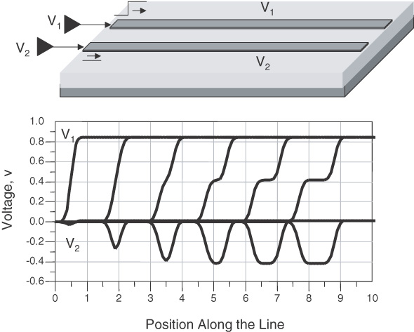
Figure 11-21 Voltage pattern on the two lines in an edge-coupled microstrip when one line is driven by a 0-v to 1-v transition and the other line is pegged low. Simulated with Agilent’s ADS.
However, in the case of an edge-coupled microstrip differential pair, there are two special voltage patterns we can launch into the pair that will propagate down the line undistorted. The first pattern is when exactly the same signal is applied to either line; for example, the voltage transitions from 0 v to 1 v in each line.
In this case, there is no dV/dt between the signal lines, so there is no capacitively coupled current. The inductively coupled current into one line is identical to the inductively coupled current into the other line since the dI/dt is the same in each line. Whatever one line does to the other, the same action is returned. The result is that as this special voltage pattern propagates down the transmission lines, the voltage pattern on either line will remain exactly the same.
The second special voltage pattern that will propagate unchanged down the differential pair is when the opposite-transitioning signals are applied to each line; for example, one of the signals transitions from 0 v to 1 v and the other goes from 0 v to −1 v.
The signal in the first line will generate far-end noise in the second line that has a negative-going pulse. This will decrease the voltage on the first line as the signal propagates. However, at the same time, the negative-going signal in the second line will generate a positive far-end noise pulse in the first line. The magnitude of the positive noise generated in line 1 is exactly the same as the magnitude of the drop in the signal in line 1 from the loss due to its noise to line 2. The result is that the voltage pattern on the differential pair will propagate down the lines undistorted. Figure 11-22 shows the voltage pattern on the two signal lines as the signal propagates down the pair of lines when these two patterns are applied.
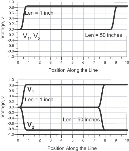
Figure 11-22 Voltage pattern on the two lines in an edge-coupled microstrip when the pair is driven in the even mode and the odd mode. The voltage pattern is the same going into the line as coming out 50 inches later. Simulated with Agilent’s ADS.
These two special voltage patterns that propagate undistorted down a differential pair correspond to two special states at which the pair of lines can be excited or stimulated. We call these special states the modes of the pair.
When a differential pair is excited into one of these two modes, the signal will have the special property of propagating down the line undistorted. To distinguish these two states, we call the state where the same voltage drives each line the even mode and the state where the opposite-going voltages drive each line the odd mode.
TIP
Modes are special states of excitation for a pair of lines. A signal that excites one of these special states will propagate undistorted down a differential pair of transmission lines. For a two-signal-line differential pair, there are only two different special states or modes. For a three-signal conductor array of coupled lines, there are three modes. For a collection of four-signal conductors and their common return path, there are four special voltage states for which a voltage pattern will propagate undistorted.
Modes are intrinsic properties of a differential pair. Of course, any voltage pattern can be imposed on a pair of lines. When the voltage pattern imposed matches one of these special states, the voltage signal propagating down the line has special properties. The modes of a differential pair are used to define the special voltage patterns.
When the two conductors in a differential pair are geometrically symmetrical, with the same line widths and dielectric spacings, the voltage patterns that excite the even and odd modes correspond to the same voltages launched in both lines and the opposite-going voltages launched into both lines. If the conductors are not symmetric (e.g., have different line widths or dielectric thickness), the odd- and even-mode voltage patterns are not so simple. The only way to determine the specific odd- and even-mode voltage patterns is by using a 2D field solver. Figure 11-23 shows the field patterns of the odd- and even-mode states for a pair of symmetric lines.

Figure 11-23 Field distribution for odd- and even-mode states of a symmetric microstrip, calculated with Mentor Graphics HyperLynx.
It is important to keep separate, on one hand, the definition of modes as special, unique states into which the pair of lines can be excited based on the geometry of the pair and, on the other hand, the applied voltages that can be any arbitrary values. Any voltage pattern can be applied to a differential pair—just connect a function generator to each signal and return path.
In the special case of a symmetric, edge-coupled microstrip differential pair, the odd-mode state can be excited by the voltage pattern corresponding to a pure differential signal. Likewise, the even-mode state can be excited by applying a pure common signal.
TIP
A differential signal will drive a signal in the odd mode, and a common signal will drive a signal in the even mode for a symmetric, edge-coupled microstrip differential pair. Odd and even modes refer to special intrinsic states of the differential pair. Differential and common refer to the specific signals that are applied to the differential pair. It’s important to note that 90% of the confusion about differential impedance arises from misusing these terms.
Introducing the terms odd mode and even mode allows us to label the special properties of a symmetric, differential pair. For example, as we saw above, the impedance a signal sees on one line depends on the proximity of the adjacent line and the voltage pattern on the other line. Now we have a way of labeling the different cases. We refer to the impedance of one line when the pair is driven in the odd-mode state as the odd-mode impedance of the line. The impedance of one line when the pair is driven in the even-mode state is the even-mode impedance of that line.
The odd mode is often incorrectly labeled the differential mode. If we equate the odd mode with the differential mode, then we might easily confuse the differential-mode impedance with the odd-mode impedance. If these were the same mode, why would there be any difference between the odd-mode impedance and the differential-mode impedance?
In fact, there is no such thing as the differential mode, so there is no such thing as the differential-mode impedance. Figure 11-24 emphasizes that we should remove the terms differential mode from our vocabulary, and then we will never be confused between odd-mode impedance and differential impedance. They are completely different quantities. There are odd-mode impedances, differential signals, and differential impedances.

Figure 11-24 There is no such thing as differential mode. Forget the words, and you will never confuse differential impedance with odd-mode impedance.
The odd-mode impedance is the impedance of one line when the pair is driven in the odd-mode state. The differential impedance is the impedance the differential signal sees as it propagates down the differential pair.
11.8 Differential Impedance and Odd-Mode Impedance
As we saw previously, the differential impedance a differential signal sees is the series combination of the impedance of each line to the return path. When there is no coupling, the differential impedance is just twice the characteristic impedance of either line. When the lines are close enough together for coupling to be important, the characteristic impedance of each line changes.
When a differential signal is applied to a differential pair, we now see that this excites the odd-mode state of the pair. By definition, the characteristic impedance of one line when the pair is driven in the odd mode is called the odd-mode characteristic impedance. As illustrated in Figure 11-25, the differential impedance is twice the odd-mode impedance. The differential impedance is thus:
where:
Zdiff = differential impedance
Zodd = characteristic impedance of one line when the pair is driven in the odd mode

Figure 11-25 The impedance between each line and its return path is the odd-mode impedance when the pair is excited with a differential signal. The differential impedance is the equivalent impedance between the two signal lines.
The way to calculate or measure the differential impedance is by first calculating or measuring the odd-mode impedance of the line and multiplying it by 2.
The odd-mode impedance is directly related to the differential impedance, but they are not the same. The differential impedance is the impedance the differential signal sees. The odd-mode impedance is the impedance of one line when the pair is driven in the odd mode.
11.9 Common Impedance and Even-Mode Impedance
Just as we can describe the impedance a differential signal sees propagating down a line, we can also describe the impedance a common signal sees propagating down a differential pair. The common signal is the average voltage between the signal lines. A pure common signal is when the differential signal is zero. This means there is no difference in voltage between the two lines, and they each have the same signal voltage.
A common signal will drive a differential pair in its even-mode state. As the common signal propagates down the line, the characteristic impedance of each line will be, by definition, the even-mode characteristic impedance. The common signal will see the two lines in parallel, as illustrated in Figure 11-26. The impedance the common signal sees will be the parallel combination of the impedances of each line. The parallel combination of the two even-mode impedances is:
where:
Zcomm= common impedance
Zeven = characteristic impedance of one line when the pair is driven in the even mode
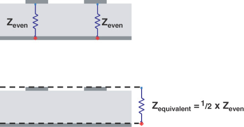
Figure 11-26 The impedance between each line and its return path is the even-mode impedance when the pair is excited with a common signal. The common impedance is the equivalent impedance between the two signal lines and the return plane.
The impedance the common signal sees is, in general, a low impedance. This is because the common signal is the same voltage as applied between each signal line and the return path, but the current going into the pair of lines and coming out the return path is twice the current going into either line. If a signal sees the same voltage but twice the current, the impedance will look half as large.
TIP
For two uncoupled 50-Ohm transmission lines that make up a differential pair, the odd- and even-mode impedances will be the same—50 Ohms. The differential impedance will be 2 × 50 Ohms = 100 Ohms, while the common impedance will be 1/2 × 50 Ohms = 25 Ohms.
As we turn on coupling, the odd-mode impedance of either line will decrease, and the even-mode impedance of either line will increase. This means the differential impedance will decrease, and the common impedance will increase. The most accurate way of calculating the differential impedance or common impedance is by using a field solver to first calculate the odd-mode impedance and even-mode impedance.
Figure 11-27 shows the complete set of impedances calculated with a field solver for the case of an edge-coupled microstrip in FR4 with 5-mil-wide traces and an uncoupled single-end characteristic impedance of 50 Ohms. As the separation between the traces gets smaller, coupling increases, and the odd-mode impedance decreases, causing the differential impedance to decrease. The even-mode impedance increases, causing the common impedance to increase. As this example illustrates, even with the tightest coupling manufacturable, the differential impedance and common impedance are only slightly affected by the coupling. The tightest coupling decreases the differential impedance in microstrip or stripline by only 10%.

Figure 11-27 All the impedances associated with a pair of edge-coupled microstrip traces, with 5-mil-wide traces in FR4 and nominally 50 Ohms, as the separation increases. Simulated with Ansoft’s SI2D.
In many microstrip traces on boards, a solder-mask layer is applied to the top surface. This will affect the single-ended impedance as well as the odd-mode impedance. Figure 11-28 shows the impedance variation for a tightly coupled microstrip differential pair as the thickness of solder mask increases. Because of the stronger field lines between the traces in the odd mode, the presence of the solder mask will affect the odd-mode impedance more than it affects the other impedances.
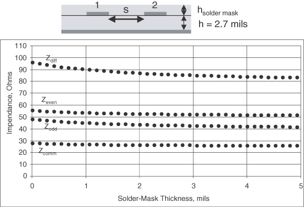
Figure 11-28 Effect on all the impedances as a solder-mask thickness applied to the top of the surface traces increases, for the case of tightest spacing of 5-mil-wide and 5-mil-spaced traces in FR4. Simulated with Ansoft’s SI2D.
This is why it is so important to take into account the presence of solder mask when designing the differential impedance of a surface trace. In addition, this effect can cause the fabricated differential impedance to be off by as much as 10%.
11.10 Differential and Common Signals and Odd- and Even-Mode Voltage Components
The terms differential and common refer to the signals imposed on a line. The part of an arbitrary signal that is the differential component is the difference between the two voltages on each signal line. The part of an arbitrary signal that is the common component is the average of the two signals on the lines.
For a symmetric differential pair, a differential signal travels in the odd mode of the pair, and a common signal travels in the even mode of the pair. We can also use the terms odd and even to describe an arbitrary signal. The voltage component of an applied signal that is propagating in the even mode, Veven, is the common component of the signal. The component propagating in the odd mode, Vodd, is the differential component of the signal. These are given by:
Likewise, any arbitrary signal propagating down a differential pair can be described as a combination of a component of the signal propagating in the even mode and a component of the signal propagating in the odd mode:
where:
Veven = voltage component propagating in the even mode
Vodd = voltage component propagating in the odd mode
V1 = signal on line 1, with respect to the common return path
V2 = signal on line 2, with respect to the common return path
For example, if a single-ended signal is imposed on one line of 0 v to 1 v and the other line is pegged low, at 0 v, the voltage component that propagates in the even mode will be Veven = 0.5 × (1 v + 0 v) = 0.5 v. The voltage component that propagates in the odd mode will be Vodd = 1 v − 0 v = 1 v. Simultaneously on the differential pair, a 0.5-v signal will be propagating down the line in the even mode, seeing the even-mode characteristic impedance of each line, and a 1-v component will be propagating down the line in the odd mode, seeing the odd-mode characteristic impedance of each line. The description of this signal in terms of odd- and even-mode components is illustrated in Figure 11-29.

Figure 11-29 Three equivalent descriptions of the same signals on a differential pair: as the voltage on each line, as the differential and common signals, and as the components propagating in the odd mode and the even mode.
Any imposed voltage can be described as a combination of an even-mode voltage component and an odd-mode component. The voltage components that travel in the odd mode are completely independent of the voltage components traveling in the even mode. They propagate independently and do not interact. Each signal component will see a different impedance for each signal line to its return path, and each signal component may also travel at a different velocity.
The examples above used an edge-coupled microstrip to illustrate the different modes. When the dielectric material completely surrounding the conductors is everywhere uniform and homogeneous, there is no longer a unique voltage pattern that propagates down the differential pair in each mode. Every voltage pattern imposed on the differential pair will propagate undistorted. After all, when the dielectric is homogeneous, as in a stripline geometry, there is no far-end cross talk. Any signal launched into the front end of the pair of lines will propagate undistorted down the line. However, by convention, we still use the voltage patterns above to define the odd and even modes for any symmetrical differential pair.
11.11 Velocity of Each Mode and Far-End Cross Talk
The description of the signal in terms of its components propagating in each of the two modes is especially important in edge-coupled microstrip because signals in each mode travel at different speeds.
The velocity of a signal propagating down a transmission line is determined by the effective dielectric constant of the material the fields see. The higher the effective dielectric constant, the slower the speed, and the longer the time delay of a signal propagating in that mode. In the case of a stripline, the dielectric material is uniform all around the conductors, and the fields always see an effective dielectric constant equal to the bulk value, independent of the voltage pattern. The odd- and even-mode velocities in a stripline are the same.
However, in a microstrip, the electric fields see a mixture of dielectric constants—part in the bulk material and part in the air. The precise pattern of the field distribution and how it overlaps the dielectric material will influence the value of the resulting effective dielectric constant and the actual speed of the signal. In the odd mode, more of the field lines are in air; in the even mode, more of the field lines are in the bulk material. For this reason, the odd-mode signals will have a slightly lower effective dielectric constant and will travel at a faster speed than do the even-mode signals.
Figure 11-30 shows the field patterns of the odd and even modes for a symmetric microstrip and stripline differential pair. In a stripline, the fields see just the bulk dielectric constant for each mode. There is no difference in speed between the modes for any homogeneous dielectric interconnect.

Figure 11-30 Electric-field distribution compared to the dielectric distribution for odd and even modes in microstrip and stripline. Simulated with Mentor Graphics HyperLynx.
In an edge-coupled microstrip, a differential signal will drive the odd mode so it will travel faster than a common signal, which drives the even mode. Figure 11-31 shows the different speeds for these two signals. As the spacing between the traces increases, the degree of coupling decreases, and the field distribution between the odd mode and the even mode becomes identical. If there is no difference in the field distributions, each mode will have the same effective dielectric constant and the same speed.
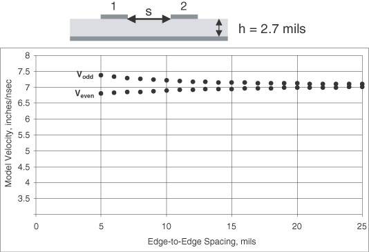
Figure 11-31 Speed of the even and odd modes for edge-coupled microstrip traces in FR4 with 5-mil-wide lines and roughly 50 Ohms.
In this example, at closest spacing, the odd-mode speed is 7.4 inches/nsec, while the even-mode speed is 6.8 inches/nsec. If a signal were launched into the line with only a differential component, this differential signal would propagate down the line undistorted at a speed of 7.4 inches/nsec. If a pure common signal were launched into the line, it would propagate down the line undistorted at a speed of 6.8 inches/nsec.
For an interconnect that is 10 inches long, the time delay for a signal propagating in the odd mode would be TDodd = 10 inches/7.4 inches/nsec = 1.35 nsec, while the time delay for an even-mode signal would be TDeven = 10 inches/6.8 inches/nsec = 1.47 nsec.
The difference of only 120 psec may not seem like much, but this small difference in delay between signals propagating in the even and odd modes is the effect that gives rise to far-end cross talk in single-ended, coupled, transmission lines.
If instead of driving the differential pair with a pure differential or common signal, we drive it with a signal that has both components, each component will propagate down the line independently and at different speeds. Though they start out coincident, as they move down the line, the faster component, typically the differential signal, will move ahead. The wavefronts of the two signals—the differential and common components—will separate. At any point along the differential pair, the actual voltage on each line will be the sum of the differential and common components. As the edges spread out, the voltage patterns on both lines will change.
Suppose we launch a voltage signal into a differential pair that has a 0-v to 1-v transition on one line, but we keep the voltage at 0 v on the other line. This is the same as sending a single-ended signal down line 1 and pegging line 2 low. Line 1 becomes the aggressor line, and line 2 becomes the victim line.
We can describe the voltage patterns on the two lines in terms of equal amounts of a signal propagating as a differential signal in the odd mode and as a common signal in the even mode. After all, a common signal of 0.5 v on line 1 and 0.5 v on line 2 and a differential signal of 0.5 v on line 1 and −0.5 v on line 2 will result in the same signal that is launched on the pair. This is shown in Figure 11-32.

Figure 11-32 Describing a signal on an aggressor line and a quiet line as a simultaneous common- and differential-signal component on a differential pair.
In a homogeneous dielectric system, such as stripline, the odd- and even-mode signals will propagate at the same speed. The two modal signals will reach the far end of the line at the same time. When they are added up again, they will recompose, with no changes, the original waveform that was launched. In such an environment, there is no far-end cross talk.
In a microstrip differential pair, the differential component will travel faster than the common component. As these two independent voltage components propagate down the differential pair, their leading-edge wavefronts will separate. The leading edge of the differential component will reach the end of line 2 before the common-signal component reaches the end of line 2.
The received signal at the far end of line 2 will be the recombination of the −0.5-v differential component and the delayed 0.5-v common-signal component. These combine to give a net, though transient, voltage at the far end of line 2. We call this transient voltage the far-end noise.
TIP
Far-end noise in a pair of coupled transmission lines can be considered to be due to the capacitively coupled current minus the inductively coupled current or the sum of the shifted differential component and the common component. These two views are perfectly equivalent.
If the leading edge of the imposed differential and common signals is a linear ramp, we can estimate the expected far-end noise due to the time delay between the two components. The setup is shown in Figure 11-33, where the voltage on line 2 is a combination of a common component and a differential component. The net voltage on line 2 is just the sum of these two components. The differential-signal and common-signal magnitudes will be exactly 1/2 the voltage on line 1, 1/2 × V1. The time delay between the arrival of the differential component (traveling in the odd mode) and the common component (traveling in the even mode) will be:

Figure 11-33 The signal on line 2 has a differential-signal component and common-signal component. The differential-signal component gets to the end of line 2 before the common component, causing a transient net signal on line 2.
The initial part of the transient signal is the leading edge of the rise time. It reaches a peak value, the far-end voltage, related to the fraction of the rise time the time delay represents:

where:
Vf = far-end voltage peak on line 2, the victim line
V1 = voltage on line 1, the aggressor line
Len = length of the coupled region
∆T = time delay between the arrival of the differential signal and the common signal
RT = signal rise time
veven = velocity of a signal propagating in the even mode
vodd = velocity of a signal propagating in the odd mode
We can interpret far-end noise as the difference in speed between the odd and even modes. If the differential pair has homogeneous dielectric and there is no difference in the speeds of the two modes, there will be no far-end noise. If there is air above the traces and the odd mode has a lower effective dielectric constant than the even mode, the odd mode will have a higher speed than the even mode has. The differential-signal component will arrive at the end of line 2 before the common component arrives. Since the differential-signal component on line 2 is negative, the transient voltage on line 2 will be negative.
As long as the time delay between the arrival of the differential and common signals is less than the rise time, the far-end noise will increase with the coupling length. However, if the time delay is greater than the rise time, the far-end noise will saturate at the differential-signal magnitude of 0.5 V1.
The saturation length of far-end noise is when Vf = 0.5 V1, which can be calculated from:
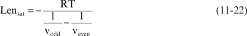
where:
Lensat = coupling length where the far-end noise will saturate
RT = rise time
veven = velocity of a signal propagating in the even mode
vodd = velocity of a signal propagating in the odd mode
For example, in the case of the most tightly coupled microstrip and a rise time of 1 nsec, the saturation length is:

The smaller the difference between the odd- and even-mode velocities, the greater the saturation length. Of course, long before the far-end noise saturates, the magnitude of the far-end noise can become large enough to exceed any reasonable noise margin.
11.12 Ideal Coupled Transmission-Line Model or an Ideal Differential Pair
A pair of coupled transmission lines can be viewed as either two single-ended transmission lines with some coupling that gives rise to cross talk on the two lines or as a differential pair with an odd- and even-mode characteristic impedance and an odd- and even-mode velocity. Both views are equivalent and separate.
In Chapter 10, we saw that the near-end (or backward) noise, Vb, and the far-end (or forward) noise, Vf, in a pair of coupled transmission lines was related to:
where:
Vb = backward noise
Vf = far-end noise
Va = voltage on the active line
kb = backward cross-talk coefficient
kf = forward cross-talk coefficient
Len = length of the coupled region
RT = rise time of the signal
Using the view of a differential pair, the cross-talk coefficients are:

The near-end noise is a direct measure of the difference in the characteristic impedance of the odd and even modes. The farther apart the traces, the smaller the difference between the odd- and even-mode impedances and the less the coupling. When the traces are very far apart, there is no interaction between the traces, and the characteristic impedance of one line is independent of the signal on the other line. The odd- and even-mode impedances are the same, and the near-end cross-talk coefficient is zero.
TIP
This connection allows us to model a pair of coupled lines as a differential pair. An ideal distributed differential pair is a new ideal circuit model that can be added to our collection of ideal circuit elements. It can model the behavior of a differential pair or a pair of independent, coupled transmission lines.
Just as an ideal, single-ended transmission line is defined in terms of a characteristic impedance and time delay, an ideal differential pair is defined with just four parameters:
1. An odd-mode characteristic impedance
2. An even-mode characteristic impedance
3. An odd-mode time delay
4. An even-mode time delay
These terms fully take into account the effects of the coupling, which would give rise to near-end and far-end cross talk. This is the basis of most ideal circuit models used in circuit or behavioral simulators.
If the transmission line is a stripline, the odd- and even-mode velocities and time delays are the same, so only three parameters are needed to describe a pair of coupled stripline transmission lines.
Usually, the parameter values for these four terms describing a differential pair are obtained with a 2D field solver.
11.13 Measuring Even- and Odd-Mode Impedance
A time-domain reflectometer (TDR) is used to measure the single-ended characteristic impedance of a single-ended transmission line. The TDR will launch a voltage step into the transmission line and measure the reflected voltage. The magnitude of the reflected voltage will depend on the change in the instantaneous impedance the signal encounters in moving from the 50 Ohms of the TDR and its interconnect cables to the front of the transmission line. For a uniform line, the instantaneous impedance the signal encounters will be the characteristic impedance of the line. The reflected voltage is related to:
where:
ρ = reflection coefficient
Vreflected = reflected voltage measured by the TDR
Vincident = voltage launched by the TDR into the line
Z0 = characteristic impedance of the line
50 Ohms = output impedance of the TDR and cabling system
By measuring the reflected voltage and knowing the incident voltage, we can calculate the characteristic impedance of the line:
This is how we can measure the characteristic impedance of any single-ended transmission.
In order to measure the odd-mode impedance or even-mode impedance of a line that is part of a differential pair, we must measure the characteristic impedance of one line while we drive the pair either into the odd mode or into the even mode.
To drive the pair into the odd mode, we need to apply a pure differential signal to the pair. Then the characteristic impedance we measure of either line is its odd-mode impedance. This means that if the incident signal transitions from 0 v to +200 mV between the line and its return path, into the line under test, we need to also apply another signal to the second line of 0-v to −200-mV between the second signal line and its return path. Likewise, measuring the even-mode characteristic impedance of the line requires applying a 0-v to +200-mV signal to both lines.
This requires the use of a special TDR that has two active heads. This instrument is called a differential TDR (DTDR). Figure 11-34 shows the measured TDR voltages with the two outputs connected to opens to illustrate how the two channels are driven when set up for differential-signal outputs and common-signal outputs.

Figure 11-34 Measured voltages from the two channels of a differential TDR when driving a differential signal (top) and a common signal (bottom) into the differential pair under test. Measured with Agilent 86100 DCA with DTDR plug-in.
In a DTDR, the reflected voltages from both channels can be measured, so the odd- or even-mode impedance of both lines in the pair can be measured. Figure 11-35 shows an example of the measured odd- and even-mode characteristic impedance of one line in a pair when the lines are tightly coupled. In this example, the odd-mode impedance is measured as 39 Ohms, and the even-mode impedance of the same line is measured as 50 Ohms.

Figure 11-35 Measured voltage (top) from one channel of a differential TDR when the output is a differential signal and a common signal. These are interpreted as the impedance of the even mode (common driven) and odd mode (differential driven). The odd-mode impedance is 39 Ohms, and the even-mode characteristic impedance is 50 Ohms. Measured with an Agilent 86100 DCA with DTDR plug-in and TDA Systems IConnect software, and a GigaTest Labs Probe Station.
11.14 Terminating Differential and Common Signals
When a differential signal reaches the open end of a differential pair, it will see a high impedance and will be reflected. If the reflections at the ends of the differential pair are not managed, they may exceed the noise margin and cause excessive noise. A commonly used method of reducing the reflections is to have the differential signal see a resistive impedance at the end of the pair that matches the differential impedance.
If the differential impedance of the line is designed for 100 Ohms, for example, the resistor at the far end should be 100 Ohms, as illustrated in Figure 11-36. The resistor would be placed across the two signal lines so the differential signal would see its impedance. The differential signal would be terminated with this single resistor. But what about the common signal?

Figure 11-36 Terminating the differential signal at the far end of a differential pair with a single resistor that has a resistance equal to the differential impedance of the pair.
TIP
While it is true that the common-signal component even in LVDS levels is very high, this voltage is nominally constant, even when the drivers are switching, and may not impact the measurement of a differential signal at the receiver.
Any transient common signal moving down the differential pair will see a high impedance at the end of the pair and reflect back to the source. Even if there were a 100-Ohm resistor across the signal lines, the common signal, having the same voltage between the two signal lines, would not see it. Depending on the impedance of the driver, any common signal created will rattle back and forth and show the effect of ringing.
Is it important to terminate the common signal? If any devices in the circuit are sensitive to the common signal, then managing the signal quality of the common signal is important. If there is an asymmetry in the differential pair that converts some differential signal into common signal, if the common signal rattles around and sees the asymmetry again, some of it may convert back into differential signal and contribute to differential noise.
TIP
Terminating the common signal will not eliminate the common signal but will simply prevent the common signal from rattling around. If a common signal is contributing to EMI, it’s true that terminating the common signal will help reduce EMI slightly, but it will still be important to create a design that eliminates the source of the common signal.
One way of terminating the common signal is by connecting a resistor between the end of each signal line and the return path. The parallel combination of the two resistors should equal the impedance the common signal sees. If the two lines were uncoupled and the common impedance were 25 Ohms, each resistor would be 50 Ohms, and the parallel impedance would be 25 Ohms. This is shown in Figure 11-37.

Figure 11-37 Terminating the common signal at the far end of a differential pair with two resistors, each with resistance equal to twice the common impedance of the pair.
If this termination scheme is used, the common signal will be terminated, and the differential signal will also be terminated. However, if the lines were tightly coupled, and the even-mode impedance were 25 Ohms, while two 50-Ohm resistors would terminate the common impedance, the differential impedance would not be terminated.
The equivalent resistance a differential signal would see in this termination scheme is the series combination of the two resistors, 4 × Zcomm. It is only when Zeven = Zodd that this resistance is the differential impedance. As coupling increases, the common impedance will increase, and the differential impedance will decrease.
If it is important to terminate the common signal and the differential signal simultaneously, we must use a special termination technique. This can be implemented with two different resistor topologies, each using three resistors. The “pi” and “tee” topologies are shown in Figure 11-38.

Figure 11-38 Pi- and tee-termination topologies for a differential pair that can terminate both the common and differential signals simultaneously.
In the pi topology, the values of the resistors can be calculated based on designing the equivalent resistance the common signal sees to equal the common impedance and the equivalent resistance the differential signal sees to equal the differential impedance. The equivalent resistance the common signal sees is the parallel combination of the two R2 resistors:
Requiv = equivalent resistance the common signal would see
R2 = resistance of each R2 resistor
Zcomm = impedance the common signal sees on the differential pair
Zeven = even-mode characteristic impedance of the differential pair
This requirement defines R2 = Zeven.
The equivalent resistance the differential signal sees is the parallel combination of the R1 resistor with the series combination of the two R2 resistors:
where:
Requiv = equivalent resistance the differential signal would see
R1 = resistance of each R1 resistor
R2 = resistance of each R2 resistor
Zdiff = impedance the differential signal sees on the differential pair
Zodd = odd-mode characteristic impedance of the differential pair
Since R2 = Zeven, we can calculate the value of R1 as:
When there is little coupling, and Zeven ~ Zodd ~ Z0, then R2 = Z0 and R1 = open. After all, with little coupling, this pi-termination scheme reduces to a simple far-end termination of a resistor equal to the characteristic impedance of either line. As the coupling increases, the resistor to the return path will increase to match the even-mode characteristic impedance. A high-value shunt resistor will short the two signal lines so the impedance the differential signal sees will drop as the coupling increases and will match the lower differential impedance.
For a typical tightly coupled differential pair, the odd-mode impedance might be 50 Ohms, and the even-mode impedance might be 55 Ohms. In this case, in a pi termination, the resistors would be 1 kOhm between the signal lines and 55 Ohms from each line to the return path. This combination will simultaneously terminate the 100-Ohm differential impedance and the 27.5-Ohm common impedance.
In a tee topology, the differential signal will see an equivalent resistance of just the series combination of the R1 resistors:
where:
Requiv = equivalent resistance the differential signal would see
R1 = resistance of each R1 resistor
Zdiff = impedance the differential signal sees on the differential pair
Zodd = odd-mode characteristic impedance of the differential pair
This defines R1 = Zodd.
The equivalent resistance the common signal sees is the series combination of the two R1 resistors that are in parallel with the R2 resistor:
The value of R2 can be extracted as:
In a tee termination, when there is little coupling, so Zeven ~ Zodd ~ Z0, the termination is simply the two R1 resistors in series between the signal lines, each equal to the odd-mode characteristic impedance. In addition, there is a center tap connection to the return path that is a short. The tee termination reduces to the pi termination in the case of no coupling. As coupling increases, the differential impedance decreases, and the R1 values decrease to match. The common impedance increases, and the R2 term increases to compensate.
If the odd-mode impedance were 50 Ohms and the even-mode impedance 55 Ohms, the tee termination would use two series resistors between the signal lines of 50 Ohms each, and it would use a 2.5-Ohm resistor between the center of the resistors and the return path.
The most important consideration when implementing a pi- or tee-termination strategy is the potential DC load on the drivers. In both cases, there is a resistance between either signal line to the return path on the order of the even-mode impedance. The lower the even-mode impedance, the more current flow from the driver. Typical differential drivers may not be able to handle low-DC resistance to the low-voltage side, so it may not be practical to terminate the common signal. Rather, care should be used to minimize the creation of common signals right from the beginning and simply to terminate the differential signals.
An alternative configuration to terminate both the differential and common signals is to use a tee topology with a DC-blocking capacitor. This circuit topology is shown in Figure 11-39. In this topology, the resistor values are the same as with a tee topology, and the value of the capacitor is chosen so that the time constant the common signal will see is long compared to the lowest-frequency component in the signal. This will ensure a low impedance for the capacitor compared with the impedance for the resistors, at the lowest-frequency component of the signal. As a first-order estimate, the capacitor value is initially chosen from:
where:
R = equivalent resistance the common signal sees
C = capacitance of the blocking capacitor
RT = rise time of the signal
Zcomm = impedance the common signal sees on the differential pair

Figure 11-39 Tee termination with DC-blocking capacitor to terminate common signals but minimize the DC-current drain.
For example, if the common impedance is about 25 Ohms, and the rise time is 0.1 nsec, the blocking capacitor should be about 10 nsec/25 Ohms = 0.4 nF. Of course, whenever an RC termination is used, a simulation should be performed to verify the optimum value of the capacitor.
Another alternative termination scheme, which works well for on-die termination, is to just terminate each signal line with a Vtt termination to a separate Vtt voltage supply. For 50-Ohm lines, this means connecting a 50-Ohm resistor to the Vtt supply. This effectively terminates each line as a single-ended transmission line.
When there is no coupling between the two signal lines, this terminates both the differential signal and the common signal, with half the power consumption of a termination to ground. As coupling increases and the differential impedance is kept to 100 Ohms, the differential signal will be terminated, and the common signal will be mostly terminated. It is not a perfect termination but can be a match to 90%.
The advantages of this approach are that it gives good differential signal termination, adequate common signal termination, and good power consumption, and it can be impedance on-die.
11.15 Conversion of Differential to Common Signals
The information content in differential signaling is carried by the differential signal. First, it is important to maintain the signal quality of the differential signal. This is done by using the following guidelines:
• Use controlled differential impedance lines.
• Minimize any discontinuities in the differential pair.
• Terminate the differential signals at the far end.
There is an additional source of distortion of the differential signal, due to asymmetries in the lines and skew between the drivers.
TIP
Distortion due to asymmetries and skews is completely independent of the degree of coupling between the lines and can occur in a differential pair with no coupling or the tightest coupling, both microstrip and stripline.
A skew between the transitioning of the two differential drivers will distort the differential signal. Figure 11-40 shows the edge of the differential signal as the skew between the drivers is increased from 20% of the rise time to two times the rise time. Most high-speed serial links specify that a line-to-line skew in a channel should be less than 20% the unit interval (UI). A line-to-line skew will directly affect the signal edges and reduce the horizontal opening of an eye.
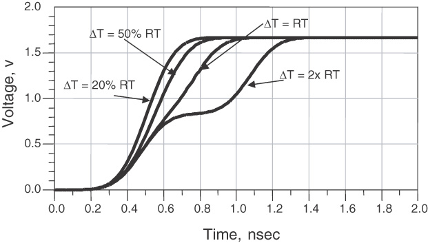
Figure 11-40 Received differential signal with driver skew varying from 20% of the rise time to 200% of the rise time. Simulated with Agilent’s ADS.
For example, in a 5-Gbps signal, the UI is 200 psec, and 20% of the UI is 40 psec, the maximum acceptable line-to-line skew. With a typical speed of a signal as 6 inches/nsec, the length difference between the two lines that make up the differential pair could be 0.04 nsec × 6 inches/nsec = 240 mils.
The line-to-line skew becomes noticeable when the skew is longer than the signal rise time. The rising and falling edges of the differential signal will be distorted.
To keep the maximum line-to-line skew below 20%, the unit interval requires:
where:
∆L = maximum length skew between paths to keep skew less than 20% of the unit interval
UI = unit interval
BR = bit rate
v = speed of the differential signal
If the speed of a signal is roughly 6 inches/nsec and the UI is 1 nsec, then the maximum length mismatch allowed in a differential pair would have to be less than 0.2 × 6 inches/nsec × 1 nsec ~ 1.2 inch. This is relatively easy to accomplish.
If the UI were 100 psec, the lengths would have to be matched to better than 120 mils. As the skew budget allocated to line-length differences decreases, it becomes more and more important to match the line lengths.
Other sources of asymmetry will potentially distort the differential signal. In general, if something affects one line and not the other, the differential signal will be distorted. For example, if one of the traces sees a test pad, so there is a capacitive load and the other trace does not, the differential signal will be distorted. Figure 11-41 shows the simulated differential signal at the end of a differential pair with a capacitive load on one line.
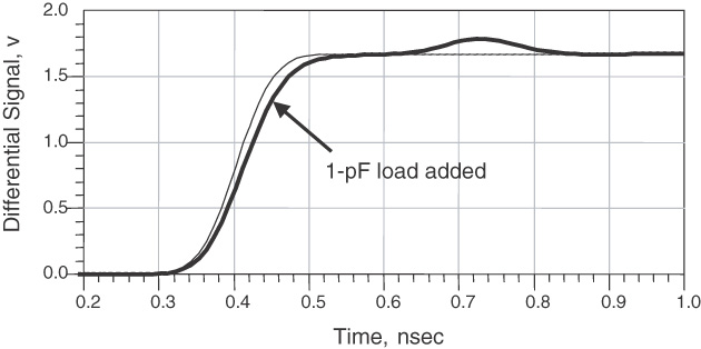
Figure 11-41 Received differential signal with and without a 1-pF capacitive load on one line of a differential pair. The rise time is 100 psec. Simulated with Agilent’s ADS.
There is another impact from skew and distortions. Any asymmetry can convert some of the differential signal into common signal. In general, if the drivers and receivers are not sensitive to common signals, the amount of common signal created may not be important. After all, differential receivers typically have a good common-mode rejection ratio (CMRR). However, if the common signal were to get out of the box on twisted pair, for example, it would dramatically contribute to EMI. It is critical to minimize any common signal that may have an opportunity, either intentionally or unintentionally, to escape outside the product enclosure through an aperture or on any cables.
TIP
Any asymmetry will convert differential signal into common signal. This includes cross talk, driver skew, length skew, and asymmetrical loading. An important motivation to keep skews to a minimum is to minimize the conversion of differential signal into common signal.
A small skew that may not affect the differential-signal quality at all can have considerable impact on the common signal. Figure 11-42 shows the voltages on the signal lines when there is a skew of just 20% of the rise time and the received differential and common signal when only the differential signal is terminated. The differential-signal component is terminated by the resistor at the far end, but the common-signal component sees an open at the far end and reflects back to the low impedance of the source. This creates the ringing.

Figure 11-42 Signals at the far end of a differential pair with a differential terminating resistor. The driver skew is only 20% of the rise time of the signal. Note the good quality of the differential signal, even with the voltage on each signal line distorted. Simulated with Agilent’s ADS.
Even if both the common and differential signals are terminated, there will still be common signal generated by any asymmetry. Figure 11-43 shows the voltages at the far end with a tee-termination network, where both differential and common signals are simultaneously terminated. The ringing is gone, but there is still a common signal, which could contribute to EMI if it were to get out of the box.

Figure 11-43 Received signals at the far end with a 20% skew and both differential- and common-signal termination. Simulated with Agilent’s ADS.
As the skew between the two signal lines increases, the magnitude of the common signal will increase, even with the common signal terminated. Figure 11-44 shows the common signal for skews of 20%, 50%, 100%, and 200% of the rise time.

Figure 11-44 Common signal generated by skew even with the common signal terminated. Skew of 20%, 50%, 100%, and 200% of the rise time. Simulated with Agilent’s ADS.
TIP
A very small driver skew can create significant common signal. This is why it is important to try to minimize all asymmetries.
To minimize the creation of common signals, care should be used to try to keep the paths as symmetrical as possible. Imperfections should be modeled to anticipate the amount of common signal created. This will allow some prediction of the severity of potential EMI problems.
11.16 EMI and Common Signals
If an unshielded twisted-pair cable, such as category-5 cable, is connected to a differential pair on a circuit board, both a differential signal and a common signal may be transmitted onto the cable. The differential signal is the intended signal that carries information content. A twisted-pair cable is a very poor radiator of electromagnetic energy from the differential signals. However, any common current on the cable will radiate and contribute to EMI.
If there is common current on the twisted pair, where is the return of the common signal? On the circuit board where the differential signal is created, the common signal will return on the return plane of the board. When the signal transitions from the circuit board to the twisted pair, there is no direct connection to the return plane of the circuit board.
This poses no problem for the differential signal. It is possible to design the differential impedance of the circuit-board interconnects to match the differential impedance of the twisted pair. The differential signal may not see any impedance discontinuity in transitioning from the board to the twisted pair.
TIP
In an unshielded twisted pair, the return path for the common signal is literally the ground or floor, or any other conductor that is nearby. The coupling to the nearest conducting surface is usually less than the coupling between adjacent signal paths, so the common impedance is usually high—on the order of a few hundred Ohms.
There may be a large impedance mismatch between what the common signal sees in the board and in the twisted pair. The connection between the two common return paths is through whatever path the current will find. At high frequency, the return path is typically dominated by stray capacitances between the circuit-board ground to the box chassis to the floor. A capacitance of only 1 pF will have an impedance at 1 GHz of about 160 Ohms. It is even lower at higher frequency, and this is for just 1 pF of stray capacitance.
As the common signal propagates down the twisted pair, the return current is continuously coupled to the nearest conductor by the stray capacitance between the twisted pair and the conductor. This is illustrated in Figure 11-45.
Figure 11-45 Schematic of the common current path when a twisted-pair cable is connected to a circuit board. The coupling paths are typically capacitive for high-frequency common-signal components.
The amount of common current on the twisted pair will depend on the common-signal voltage launched into the cable and on the impedance the common signal sees in the cable:
This common current will radiate. The amount of common current that will fail a certification test depends on the specific test spec, length of cable, and frequency. As a rough rule of thumb, it takes only 3 microAmps of common current, at 100 MHz, in a 1-meter-long external cable to fail an FCC Class B certification test. This is a tiny amount of common current.
If the radiated field strength exceeds the allowed limits of the EMI certification regulation, the product will not pass certification, and this may delay the ship date of the product. In most countries, it is illegal to sell a product for revenue unless it has passed the local certification regulations. In the United States, the Federal Communications Commission (FCC) specifies the acceptable radiated field levels in two categories of products. Class A products are those that will be used in an industrial or manufacturing environment. Class B products are those that will be used in a home or office environment. Class B requirements limit acceptable radiated emissions to lower levels than Class A requirements.
Electric-field strength is measured in units of volts/m at a specified frequency. For Class B certification, the maximum radiated field strengths are measured 3 m from the product. The maximum electric-field strengths vary within different frequency ranges. They are listed and plotted in Figure 11-46. As a reference point, the maximum acceptable field strength at 3 m for 100 MHz is 150 microV/m.

Figure 11-46 FCC Class B certification limits for the maximum allowable far-field electric-field strengths at a distance of 3 m.
We can estimate the radiated electric-field strength from a common signal in a twisted pair by approximating the twisted pair as an electric monopole antenna. The far field exists at a distance about one-sixth of the wavelength of the radiation. The FCC test condition of 3 m is in the far field for frequencies larger than about 16 MHz. The far-field electric-field strength from an electric monopole antenna is:
where:
Icomm = common current on the twisted pair, in Amps
Vcomm = common signal that is launched into the twisted pair
Zcomm = impedance the common signal sees
E = field strength at a distance R from the wire, in volts/m
f = sine-wave frequency of the common current component, in Hz
Len = length of the twisted wire that is radiating, in m
R = distance from the wire to the point where the field is measured, in m
For example, if the common signal is 100 mV and the impedance the common signal sees in the twisted pair is 200 Ohms, the common current may be as large as 0.1 v/200 Ohms = 0.5 mA. If the length of the twisted pair is 1 m and the distance at which we measure the field strength is 3 m, corresponding to the FCC Class B test, the radiated field strength at 100 MHz is:
The radiated field strength from a common current that might easily be generated in an unshielded twisted pair is more than a factor of 100 larger than the FCC Class B certification limit.
TIP
Even small amounts of common currents getting onto an unshielded twisted-pair cable can cause a product to fail an EMI certification test. Common currents larger than about 3 microAmps will fail FCC Class B Certification.
There are generally three techniques to reduce the radiated emissions from common currents in twisted-pair cables:
1. Minimize the conversion of differential signal into common signal by minimizing any asymmetries in the differential pairs and skews in the drivers. This minimizes the problem at the source.
2. Use a shielded twisted pair so the return path of the common current in the twisted pair is carried in the shield. Using a shielded cable may even increase the amount of common current since the common impedance may be lowered with the return path brought closer to the signal path. If the shield is connected to the chassis, the return current of the common signal may have an opportunity to flow on the inside of the shield. The common signal would then be flowing in a coax geometry—going out on the cable on the twisted-pair center and back on the inside of the shield. In this geometry, there would be no external magnetic or electric field, and the common current would not radiate. This requires using a low-inductance connection between the shield and the chassis so that the common-return current can maintain its coaxial distribution.
3. Increase the impedance of the common-current path by adding common chokes. Common signal chokes are of two forms. Virtually all cables used by peripherals have cylinders of ferrite material on the outside of the cable. The placement of a ferrite around a cable is shown in Figure 11-47. The high permeability of the ferrite will increase the inductance and the impedance of any net currents going through the ferrite. In addition, many RJ45 connectors used in Ethernet links have common-mode ferrite chokes built in.
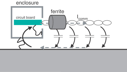
Figure 11-47 Placement of ferrite around the differential currents but enclosing only the common signal path, not the common return path.
If a differential signal flows through the ferrite, there will be no net magnetic field through the ferrite. The currents in each line of the differential pair are equal and in opposite directions, so their external magnetic and electric fields mostly cancel each other. Only common-signal currents going through the ferrite, with return currents on the outside, would have magnetic-field line loops that would go through the ferrite material and see a higher impedance. The ferrite on the outside of the cable increases the impedance the common signal sees, reducing the common current, which decreases the radiated emissions. This type of ferrite choke can be used on the outside of any cable—twisted pair or shielded.
The second type of common-signal choke is primarily useful for twisted-pair cable and is often built into the connector. Connectors with a built-in choke are sometimes called “magnetics.” The goal is to dramatically increase the impedance a common signal would see but not affect the impedance a differential signal would see. To radically increase the impedance of the common signal, a twisted-pair wire is wound into a coil, sometimes with a ferrite core.
Any common current flowing down the twisted pair will see a much higher inductance from the coiling and the high-permeability ferrite core. However, the differential signal on the twisted pair will have very few magnetic-field lines outside the twisted pair, and the differential current will not see the coil or the ferrite. The differential signal will be nearly unaffected by the coiling.
A twisted-pair coil can be built into a connector. Many RJ-45 connectors, used with Ethernet cables, for example, have built-in common-signal chokes.
TIP
The higher impedance seen by the common signal can reduce the common current that would get onto the twisted-pair cable by more than 99%, or −40 dB. They are essential components to minimize radiated emissions from any common currents created by asymmetries in the circuit board.
11.17 Cross Talk in Differential Pairs
If we bring a single-ended transmission line close to a differential pair, some of the signal voltage will couple from the active, single-ended line to both lines of the differential pair. This is illustrated in Figure 11-48. The noise that couples to each line of the differential pair will be the same polarity, just of different magnitudes.

The closer line of the pair will end up with more noise than the farther line. The more tightly coupled the differential pair, the more equal the noise generated on the two lines, and the less the differential noise.
TIP
In general, the more identically we can arrange the noise that is picked up on each line of the pair, the less the differential noise. This generally means a configuration of tightly coupled lines, with a large space between the pair and the aggressor line.
Figure 11-49 shows the differential noise at the receiver generated on the differential pair constructed in stripline, with the far end differentially terminated and the near end having the low impedance of a typical driver.
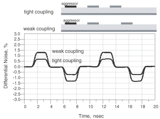
Figure 11-49 Differential noise in a differential pair from an adjacent single-ended aggressor line.
In this configuration, the aggressor line is spaced a distance equal to the line width away from the nearest victim trace. Two different coupling levels are evaluated. Tight coupling has a spacing between lines in the differential pair equal to the line width, while weak coupling has spacing twice the line width. In the pair, the line that is farther away from the aggressor will have slightly less noise coupled to it than the line close to the aggressor line. The differential noise is the difference between the noise levels on the lines. In this example, there is about 1.3% differential noise on the weakly coupled victim differential pair, while there is about half this value on the tightly coupled victim differential pair. Tighter coupling can decrease the differential noise by about 50%.
Though the differential noise from the active line to the differential line may be only 1.3% in the worst case, this may sometimes cause problems. If the aggressor line is a 3.3-v signal level, the differential noise on the differential pair may be as large as 40 mV. If there is another active line on the other side of the victim lines, switching in the opposite direction of the first aggressor line, the differential noise from the two active lines will add to the victim line. This can contribute as much as 80 mV of noise, which may approach the allocated noise budget for some low-voltage differential signals.
The common noise on the victim differential pair is the average voltage on each line. Figure 11-50 shows the common noise for the two levels of coupling. The common noise will not be strongly affected as the coupling between the differential pair changes. With tight coupling (i.e., a spacing equal to the line width), the common noise is about 2.1%. With weak coupling (i.e., a spacing in the differential pair equal to twice the line width), the common noise is reduced to about 1.5%.
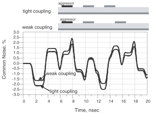
Figure 11-50 Common noise in a differential pair from an adjacent single-ended aggressor line. The ringing and distortion are due to the common signal not being terminated.
Tighter coupling will decrease the differential noise but increase the common noise. Cross talk is one of the typical ways that common currents are created on a differential pair. Even if the differential pair is designed for perfect symmetry, cross talk can cause the creation of common voltages on a differential pair. This is why it is always important to provide common-signal chokes for any externally connected twisted-pair cables.
TIP
This suggests the general rule that to minimize the differential noise on a differential pair from a single-ended aggressor line, the coupling in the differential pair should be as tight as possible. Of course, the spacing between the aggressor and the victim pair should also be as large as possible to minimize the coupled noise. Tight coupling will not eliminate cross talk but will just reduce it in some cases.
The differential noise coupling between two differential pairs is slightly less than the differential noise coupling from a single-ended line. Figure 11-51 shows the differential and common noise between two differential pairs. In this case, the edge-to-edge spacing between the two pairs is equal to the line width. The difference between tight and weak coupling is not very large. As a rough estimate, the differential noise can be less than 1%, and the common noise can be less than 2% of the differential signal on the aggressor pair.
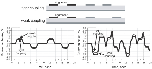
Figure 11-51 Differential (left) and common (right) noise on a differential pair when the aggressor line is also a differential pair for the case of tight and weak coupling within the victim pair.
Generally, the coupling in a differential pair, especially in stripline, has only a small effect on the differential cross talk picked up on the pair from another trace. It is only when there is not adjacent return plane, such as in a connector or leaded package, that tight coupling will have a strong impact on reducing cross talk.
11.18 Crossing a Gap in the Return Path
Gaps in the return path are often used to isolate one region of a board from another. They also occur when a power plane is used as the reference layer and when a split power layer is used. Sometimes, a gap in the return path occurs unintentionally, as when the clearance holes in a return plane are over-etched and overlap. In this case, any signal lines that pass through the via field will see a gap in the return path.
A single-ended signal will see a potentially disastrous discontinuity if the gap it encounters is wide. This will look like a large inductive discontinuity. Figure 11-52 shows the simulated reflected and transmitted single-ended signal passing over a 1-inch gap in the return path of an otherwise uniform 50-Ohm line with terminations at each end. The 100-psec initial rise time is dramatically increased due to the series inductive discontinuity.

Figure 11-52 Reflected and transmitted 100-psec signal through a 50-Ohm transmission line with a 1-inch-wide gap in the return path in the middle. Simulated with Mentor Graphics HyperLynx.
While it may be possible in some situations to use a low-inductance capacitor to span the gap and provide a lower-impedance path for the return, it is difficult to get good high-frequency performance.
An alternative approach to transport a signal across a gap in the return path with acceptable performance is using a differential pair. Figure 11-53 illustrates a typical case where the signal starts in one region of a board as an edge-coupled microstrip differential pair, in a second region where the return plane is far away, and in a third region where the interconnect is again an edge-coupled microstrip.
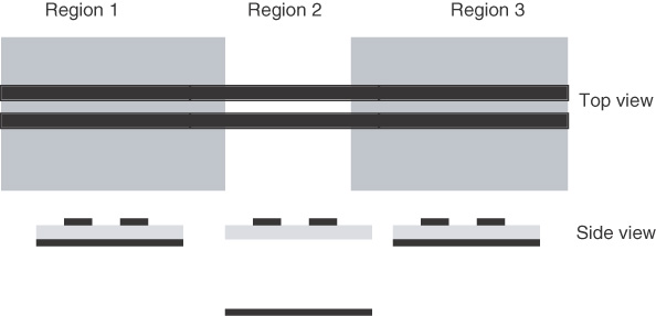
Figure 11-53 Region 2 of a circuit board is where there is a gap in the return path. This can be modeled as a region where the return path is very far away.
In regions 1 and 3, the differential pair has a differential impedance of about 90 Ohms. In the middle region, the return path is removed. With a 5-mil line and space and a 2.7-mil dielectric beneath the traces, but no other conductor, the differential impedance is about 160 Ohms. If the return plane is at least as far away as the span of the signal conductors, the differential impedance will be independent of the position of the return plane, and it is as though it is not there. This trick allows us to build a circuit model for this discontinuity and to explore the impact of the discontinuity on the differential-signal quality. Figure 11-54 shows the simulated reflected and transmitted differential signal passing through the same gap as before. The rise time is preserved in the transmitted differential signal.

Figure 11-54 Differential signal with a 100-psec rise time transmitted and reflected across a 1-inch-wide gap in the return plane. The differential signal is minimally distorted across the gap. Simulated with Mentor Graphics HyperLynx.
TIP
Using a tightly coupled differential pair is one way of transmitting high-bandwidth signals in regions with poorly defined return planes.
While the 160-Ohm differential impedance in the region of the gap is higher than the 90-Ohm differential impedance of the rest of the interconnect, it is a uniform transmission line. This will cause a degradation of signal quality. More importantly, single-ended signals, in passing over the gap in the return path, will create ground bounce as their return currents will see the common inductance of the gap. However, differential signals will have their return currents overlap in the common inductance and mostly cancel. With virtually no net return current crossing the gap, the ground bounce from differential signals will be dramatically less than for single-ended signals.
11.19 To Tightly Couple or Not to Tightly Couple
A differential pair can transport a differential signal just as well if the coupling between the pairs is tight or loose, provided that the differential impedance is the same. Of course, in fabricating for a target differential impedance, the cross section and stack-up must take into account the coupling. With an accurate 2D field-solver tool, the stack-up for any target differential impedance and any level of coupling is equally easy to design.
This means that from a differential signal’s perspective, as long as the instantaneous differential impedance is constant, it doesn’t matter what the coupling is. The two lines that make up the pair can come close together and then move far apart, as long as the line width is adjusted to always maintain 100 Ohm differential impedance.
The most important advantage of using tightly coupled differential pairs is the higher interconnect density with tight coupling. This means either fewer layers or potentially a smaller board, both of which could contribute to lower cost. If there are no other important considerations, tightly coupled differential pairs should always be the first choice because they can result in the lowest-cost board.
In some cases, the differential cross talk to a tightly coupled pair might be a little less than if loosely coupled. However, this is not universally true so should be considered on a case-by-case basis.
The other advantage of tightly coupled differential pairs is that the signal is robust to imperfections in the return path. As a general rule, whenever the return planes are disrupted, such as in twisted-pair cables, ribbon cables, connectors, and some IC packages, tight coupling should always be used. For these reasons, tight coupling should always be the first choice. However, tight coupling may not be the best choice in every design.
In comparing the line width of a loosely coupled and tightly coupled 100-Ohm differential pair, the line width has to decrease about 30% to maintain the 100 Ohms. This means a loosely coupled pair will have about 30% lower series-resistive loss than a similar-impedance tightly coupled pair. When loss is important, this can be an important reason to use loosely coupled pairs. Generally, above 10 Gbps, when loss is the most important performance term, loosely coupled differential pairs will enable the widest lines and the lowest loss and should be the first choice.
The most significant advantage of using loosely coupled lines is the opportunity to use a wider line width. If we start with a differential pair that is loosely coupled and bring the traces closer together, keeping everything else the same, the differential impedance will decrease. To achieve the target impedance, we have to make the lines narrower. This means higher resistance lines.
TIP
When cost is the driving force, tightly coupled differential pairs should be used. When loss is important, loosely coupled differential pairs should be used.
11.20 Calculating Odd and Even Modes from Capacitance- and Inductance-Matrix Elements
The first-order model of a single-ended transmission line is an n-section lumped-circuit model. This is described in terms of a capacitance per length and a loop inductance per length. The characteristic impedance and time delay of a single-ended transmission line are given by:

where:
Z0 = single-ended characteristic impedance of the line
LL = loop inductance per length of the line
CL = capacitance per length of the line
TD = time delay of the line
We can extend this model to include the coupling between two lines. Figure 11-55 shows the equivalent circuit model of a section of the two coupled transmission lines. The capacitor elements are defined in terms of the SPICE capacitor matrix, and the inductance elements are defined in terms of the loop-inductance matrix. Of course, the values of the C and L matrix elements are obtained directly from the stack-up geometry of the differential pair by using a 2D field solver tool. We can use this model to determine the even- and odd-mode characteristic impedance values based on the values of the matrix elements.

Figure 11-55 One section of an n-section lumped-circuit model for a pair of coupled transmission lines, with the SPICE capacitance matrix and a loop-inductance matrix that defines all the model elements.
When the pair is driven in the odd-mode state, the impedance of one line is the odd-mode characteristic impedance. The equivalent capacitance of one line is:
where:
Codd = capacitance per length from the signal to the return path of one line when the pair is driven in the odd mode
C11 = diagonal element of the SPICE capacitance matrix
C12 = off-diagonal element of the SPICE capacitance matrix
Cload = loaded capacitance of the signal line = C11 + C12
In the odd mode, current is going into the signal line of trace 1 and back out its return path. At the same time, current is coming out of line 2 and into its return path. In this configuration, around transmission line 1 will be mutual magnetic-field lines from the signal in transmission line 2; these mutual magnetic-field lines are going opposite to the self-field lines of line 1. The equivalent loop inductance of line 1 will be reduced due to the current in line 2. The equivalent loop inductance of line 1 when the pair is driven in the odd mode is:
where:
Lodd = loop inductance per length from the signal to the return path of one line when the pair is driven in the odd mode
L11 = diagonal element of the loop-inductance matrix
L12 = off-diagonal element of the loop-inductance matrix
Looking into line 1 of the pair, we see a higher capacitance and lower loop inductance as the coupling between the lines increases. From these two terms, the odd-mode characteristic impedance and time delay can be calculated as:

When the pair is driven in the even mode, the capacitance between the signal and the return is reduced due to the shielding from the adjacent trace driven at the same voltage as trace 1. The equivalent capacitance per length is:
Ceven = capacitance per length from the signal to the return path of one line when the pair is driven in the even mode
C11 = diagonal element of the SPICE capacitance matrix
C12 = off-diagonal element of the SPICE capacitance matrix
Cload = loaded capacitance of the signal line = C11 + C12
When driven in the even mode, current goes into signal line 1 and back out its return path. At the same time, current also goes into signal line 2 and back out its return path. The magnetic mutual-field lines from line 2 are in the same direction as the self-field lines in line 1. The equivalent loop inductance of line 1 when driven in the even mode is:
where:
Leven = loop inductance per length from the signal to the return path of one line when the pair is driven in the even mode
L11 = diagonal element of the loop-inductance matrix
L12 = off-diagonal element of the loop-inductance matrix
From the capacitance per length and loop inductance per length looking into the front of line 1 when the pair is driven in the even mode, we can calculate the even-mode characteristic impedance and time delay:
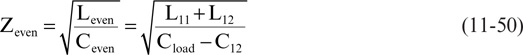
These relationships based on the capacitance- and inductance-matrix elements are used by all field solvers to calculate the odd- and even-mode characteristic impedances and the time delays for any transmission, with any degree of coupling and any stack-up configuration. In this sense, the capacitance- and inductance-matrix elements completely define the electrical properties of a pair of coupled transmission lines. This is a more fundamental description that shows the underlying effect of how the off-diagonal terms, C12 and L12, that describe coupling affect the characteristic impedance and time delay for each mode. As coupling increases, the off-diagonal terms increase, the odd-mode impedance decreases, and the even-mode impedance increases.
11.21 The Characteristic Impedance Matrix
There is an alternative description of two or more coupled transmission lines that uses an impedance matrix. This is just as fundamental as the use of the capacitance and inductance matrices; it’s just different. In this description, an impedance matrix is defined that relates the current and voltage into either line of a differential pair. Though the following analysis illustrates the impedance matrix for two coupled lines, it can be generalized to n coupled lines. It applies no matter what the stack-up geometry, symmetry, or materials distribution. These features will affect the parameter values but not the general approach.
Two transmission lines are shown in Figure 11-56. Any arbitrary signal into either line can be described by the voltage between each line and the current into each signal line and out its return path. If there were no coupling between the lines, the voltage on each line would be independent of the other line. In this case, the voltages on each line would be given by:
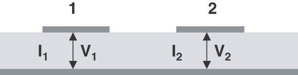
Figure 11-56 The voltage on each line and the current into each signal line and back out the return are labeled as shown.
However, if there is some coupling, this cross talk will cause the voltage on one line to be influenced by the current on the other line. We can describe this coupling with an impedance matrix. Each element of the matrix defines how the current into one line and out its return path influences the voltage in the other line. With the impedance matrix, the voltages on line 1 and 2 become:
The diagonal elements of the impedance matrix are the impedances of each line when there is no current into the other line. Of course, when the coupling is turned off, the diagonal elements reduce to what we have called the characteristic impedance of the line.
The off-diagonal elements of the impedance matrix describe the amount of coupling but in a non-intuitive way. These are matrix elements. They are not the actual impedance between line 1 and line 2. Rather, they are the amount of voltage generated on line 1 per Amp of current in line 2. In this sense, they are really mutual impedances:

When there is little coupling, no voltage is created on one line for any current in the other line, and the off-diagonal element between the lines is nearly zero. The smaller the off-diagonal term compared to the diagonal term, the smaller the coupling.
From this description, we can identify the odd- and even-mode impedances in terms of the characteristic impedance matrix. When a pure differential signal is applied to the two lines, the odd mode is driven. The odd mode is defined as when the current into one line is equal and opposite to the current into the other line, or I1 = –I2. Based on this definition, the voltages are:
From this, we can calculate the odd-mode impedance of line 1:
Likewise, the even mode is when the currents into each line are the same, I1 = I2. The voltage on line 1 in the even mode is:
The even-mode impedance of line 1 is:
In the same way, the odd- and even-mode impedance of the other line can be found. In this definition, the odd-mode impedance of one line is the difference between the diagonal and off-diagonal impedance-matrix elements. The larger the coupling, the larger the off-diagonal element and the smaller the differential impedance. The even-mode impedance of one line is the sum of the diagonal and off-diagonal impedance-matrix elements. As coupling increases, the off-diagonal element increases, and the even-mode impedance gets larger.
Most 2D field solvers report the odd- and even-mode impedance, the capacitance and inductance matrices, and the impedance matrix.
From a signal’s perspective, the only things that are important are the differential and common impedances, which can be described in three equivalent ways by:
1. Odd- and even-mode impedances
2. Capacitance- and inductance-matrix elements
3. Impedance matrix
These are all separate and independent ways of describing the electrical environment seen by the common and differential signals.
11.22 The Bottom Line
1. A differential pair is any two transmission lines.
2. Differential signaling has many signal-integrity advantages over single-ended signals, such as contributing to less rail collapse, less EMI, better noise immunity, and less sensitivity to attenuation.
3. Any signal on a differential pair can be described by a differential-signal component and a common-signal component. Each component will see a different impedance as it propagates down the pair.
4. The differential impedance is the impedance the differential signal sees.
5. A mode is a special state in which a differential pair operates. A voltage pattern that excites a mode will propagate down the line undistorted.
6. A differential pair can be fully and completely described by an odd-mode impedance, an even-mode impedance, and a time delay for the odd mode and for the even mode.
7. The odd-mode impedance is the impedance of one line when the pair is driven in the odd mode.
8. Forget the words differential mode. There is only odd mode, differential signal, and differential impedance.
9. Coupling between the lines in a pair will decrease the differential impedance.
10. The only reliable way of calculating the differential or common impedance is with an accurate 2D field solver.
11. Tighter coupling will decrease the differential cross talk picked up on a differential pair and will minimize the discontinuity the differential signal sees when crossing a gap in the return plane.
12. One of the most frequent sources of EMI is common signals getting onto an external twisted-pair cable. The way to reduce this is to minimize any asymmetries between the two lines in a differential pair and add a common-signal choke to the external cable.
13. All the fundamental information about the behavior of a differential pair is contained in the differential and common impedance. These can be more fundamentally described in terms of the even and odd modes, in terms of the capacitance and inductance matrices, or in terms of the characteristic impedance matrix.
End-of-Chapter Review Questions
11.1 What is a differential pair?
11.2 What is differential signaling?
11.3 What are three advantages of differential signaling over single-ended signaling?
11.4 Why does differential signaling reduce ground bounce?
11.5 List two misconceptions you had about differential pairs before learning about differential pairs.
11.6 What is the voltage swing in LVDSsignals? What is the differential signal?
11.7 Two single-ended signals are launched into a differential pair: 0 V to 1 V and 1 V to 0 V. Is this a differential signal? What is the differential signal component, and what is the common signal component?
11.8 List four key features of a robust differential pair.
11.9 What does differential impedance refer to? How is this different from the characteristic impedance of each line?
11.10 Suppose the single-ended characteristic impedance of two uncoupled transmission lines is 45 Ohms. What would a differential signal see when propagating on this pair? What common impedance would a signal see on this pair?
11.11 Is it possible to have a differential pair with the two signal lines traveling on opposites ends of a circuit board? What are three possible disadvantages of this?
11.12 As the two lines that make up a differential pair are brought closer together, the differential impedance decreases. Why?
11.13 As the two lines that make up a differential pair are brought closer together, the common impedance increases. Why?
11.14 What is the most effective way of calculating the differential impedance of a differential pair? Justify your answer.
11.15 Why is it a bad idea to use the terms differential mode impedance and common mode impedance?
11.16 What is odd-mode impedance, and how is it different from differential impedance?
11.17 What is even-mode impedance, and how is it different from common impedance?
11.18 If two lines in a differential pair are uncoupled and their single-ended impedance is 50 Ohms, what are their differential and common impedances? What happens to each impedance as the lines are brought closer together?
11.19 If two lines in a differential pair are uncoupled and their single-ended impedance is 37.5 Ohms, what are their odd mode and even mode impedances?
11.20 If the differential impedance in a tightly coupled differential pair is 100 Ohms, is the common impedance higher, lower, or the same as 25 Ohms?
11.21 In a tightly coupled differential microstrip pair, where is most of the return current?
11.22 List three different interconnect structures in which the return current of one line of a differential pair is carried by the other line.
11.23 In stripline, how does the speed of the differential signal compare to the speed of the common signal as the two lines are brought closer together? How is this different in stripline?
11.24 Why is it difficult to engineer a perfectly symmetrical differential pair in broadside-coupled stripline?
11.25 What happens to the odd mode loop inductance per length as the two lines in a microstrip differential pair are brought closer together? What about the loop inductance of the even mode? How is this different in microstrip?
11.26 If you only used a 100-Ohm differential resistor at the end of a 100-Ohm differential pair, what would the common signal do at the end of the line?
11.27 Why is on-die Vtt termination of each line separately an effective termination strategy for a differential pair? If each resistor is 50 Ohms and the differential impedance is 100 Ohms, what might be the worst-case reflection coefficient of the common signal if the two lines are tightly coupled?