
3. Signal Path Analysis as an Aid to Signal Integrity
Signal integrity is a growing priority as digital system designers pursue ever-higher clock and data rates in computer, communications, video, and network systems. At today's high operating frequencies, anything that affects a signal's rise time, pulse width, timing, jitter, or noise content can influence reliability at the system level. To ensure signal integrity, it is essential to understand and control impedance in the transmission environment through which signals travel.
The development of true analog CMOS processes has led to the use of high-speed analog devices in the digital arena. High clock speeds have become common for digital logic. Systems considered high-end and high-speed a few years ago are now easy and inexpensive to implement in the new CMOS technology. However, this integration of fast edge rates and system speeds brings the challenges of analog system design to a digital world. "High-speed" does not just mean faster communication rates—say, faster than 1 gigabit per second (Gbps). More importantly, a signal with a 600-picosecond rise time is also a high-speed signal. This opens the entire printed circuit board (PCB) to careful and targeted board simulation and design. The designer must consider any discontinuities on the board. Some common sources of discontinuities are vias, right-angled bends, and passive connectors.
A relatively low-frequency digital signal or, more importantly, a signal with slow edge rates, may see a connecting wire or PCB trace as an ideal connection without resistance, capacitance, or inductance. Moreover, a relatively high frequency, or fast edge, signal could similarly see a well-designed short section of PCB track as an ideal connection. Consequently, the signal integrity engineer carefully needs to determine specific signal and connection parameters to establish whether a connection will be transparent to a signal or, more importantly, if the connection will exhibit transmission line properties. Digital signals with fast edge rates are our main concern, because they create connection path conditions where analog circuit characteristics dominate, causing impedances, inductances, and capacitances to become principal characteristics in the signal transmission path. These SI issues are a secondary consequence of Moore's Law, which has been the driving force in modern microprocessor and digital design for a number of decades. The twofold increase in system speed every eighteen months has constantly reduced signal timing budgets. Today Moore's Law manifests itself as a significant decease in signal rise times that currently results in a corresponding increase in signal integrity issues. Edge rates are now a pivotal concern in the SI engineering of data transmission paths.
The traditional method of assessing transmission line parameters or signal path discontinuities is to apply sinusoidal waves to the line and measure the resultant analog signals. Frequency response techniques allow engineers to determine a line's standing wave ratio, which is the ratio of the incident signal to the reflected signal, and other frequency domain characteristics. Likewise, a number of modern test instruments, such as vector network analyzers (VNAs), accurately measure the frequency domain scatter parameters (S-parameters) of two-port networks, such as a transmission line. However, digital design engineers essentially live in the time domain, where they instinctively design and interpret time-related signals and intuitively perform time domain measurements with oscilloscopes and logic analyzers. Therefore, this chapter introduces the concept of transmission line impedance and other signal path parameters by intuitive time domain reflectometry (TDR) measurement methodology. Although this chapter focuses on TDR, it is important to note that the frequency domain and S-parameters are significant measurements in the characterization of a modern high-speed communication channel. Today many TDR systems feature built-in mathematical functions and specialist integrated software that provide both time and frequency information. Even so, there is often a need for both TDR and VNA measurements. Consequently, this chapter considers the merits of both TDR and VNA but focuses on time domain measurements as a vehicle to intuitively understand modern high-speed digital signal path design.
3.1. The Transmission Line Environment
A common definition of a PCB transmission line is the signal path or conductive connection between a digital transmitter and receiver. Traditionally, transmission lines were telecommunication cables operating over long distances, and reflected signals appeared as annoying echoes that often made a line inoperable. However, with high-speed digital signal transmission, even the shortest passive PCB trace can exhibit transmission line effects. Transmission line theory encompasses electromagnetic field concepts and generally attracts complex mathematical analysis. With TDR, the engineer can intuitively understand what is happening with his device. It is important for the signal integrity engineer to acquire equally intuitive insight into transmission line theory, even though some of the basic concepts require a few simple calculations. In transmission line theory, we need to consider the propagation characteristics of a connection from the viewpoint of a digital signal as it traverses the connection system. The signal path in this case is a linear passive connection system that is simply called the interconnection. It often consists of a complex signal path, such as a printed circuit board trace, cable, IC package, flexible PCB, and connectors.
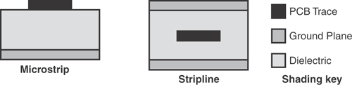
As an example, consider Figure 3-1, which shows two commonly used PCB transmission line topologies. If an electromagnetic signal, such as a wireless signal, travels in free space, typically it would have the velocity of light, which is 3.108 meters per second. As a signal enters a denser transmission medium, such as a visible ray of light passing through glass, the signal would slow to a lower velocity. The microstrip PCB topology has one half of its track in free space and the other half bounded by a dielectric, compared to a stripline PCB track, which is surrounded by a dielectric. This makes the signal velocity calculation for the microstrip somewhat more complicated. The simplified calculation for the signal velocity for stripline is the ratio of the speed of an electromagnetic signal in free space to the square root of the dielectric constant of the material surrounding the PCB trace.
Figure 3-1. Cross sections of microstrip and stripline PCB transmission line topologies.
Therefore, the velocity (v) of a signal in stripline is
Equation 3-1
![]()
where c is the speed of light in free space (3.108 meters per second) and er is the dielectric constant of the material surrounding the PCB trace.
A common PCB dielectric material is FR4, which has a dielectric constant in the region of 4.
We can put some values into Equation 3-1 and determine the approximate velocity of a signal in stripline, assuming a dielectric constant of 4:
![]()
Given that 1 inch equals 2.54 cm:
![]()
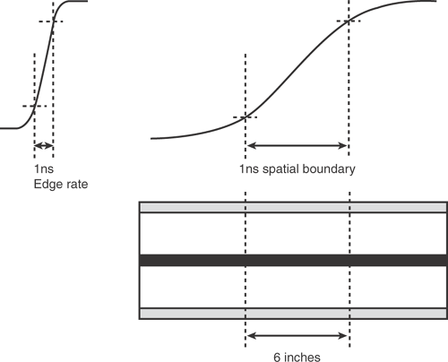
Therefore, the velocity of the signal in stripline is on the order of 5.9.109 inches per second, which is approximately 6 inches per nanosecond. The velocity of microstrip is somewhat faster at about 7 inches, or more, per nanosecond.
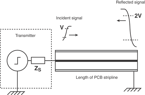
The implication of this important calculation is that a digital signal with a 1 ns rise time would take about 6 inches of stripline to reach its full amplitude. In other words, the spatial boundary of the 1 ns edge would be approximately 6 inches as the digital signal propagates along the stripline, as shown in Figure 3-2.
Figure 3-2. A 1 nanosecond leading edge applied to a length of stripline.
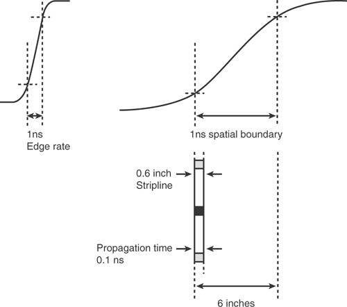
When does a PCB track become a transmission line? It depends on the signal rise time and the electrical length of the interconnection that the signal is propagating. For example, if the signal rise time is one tenth of the interconnection propagation delay, the interconnection most likely will exhibit transmission line properties.
The key concept shown in Figure 3-3 is that the leading edge of the digital signal has a spatial boundary that is long enough to be unaffected by the electrical characteristics of the stripline. In essence, the 1 ns edge becomes a 6-inch leading edge traversing the short length of stripline. In this case, the stripline is more or less transparent to the signal. From a signal integrity point of view, this is a good thing. Of course, if you wanted to troubleshoot or determine the characteristics of a short length of interconnect by way of a fast edge, such as the case when using TDR, you would have to use an instrument that generated a step pulse with a rise time that is sufficiently faster than the interconnect's propagation delay. To use a digital edge to expose multiple discontinuities in a transmission line, as is the case with TDR, we have to apply a digital edge with a rise time that is at least twice as fast as the propagation delay between discontinuities.
Figure 3-3. A 1 nanosecond leading edge applied to a 0.6-inch length of stripline.
3.2. Characteristic Impedance, Reflections, and Signal Integrity
Today engineers develop digital systems such as computers and telecommunication networks that depend on reliable high-speed digital data transmission and reception. An important part of developing such a system is the complete communication channel analysis to confirm the system's signal integrity. The linear passive interconnect between a transmitter and receiver is often analyzed as a transmission line. In addition, the effects of the digital transmitter and receiver interface circuitry have to be considered, because they can have a significant effect on the data that propagates throughout the whole channel. As we have seen at low frequencies, or slow edge rates, the frequency response of the transmission line has little influence on the signal, unless the interconnection path is particularly long. However, as signal frequencies increase and edge rates decrease, the frequency response of the transmission environment as a whole, including transmitter and receiver, takes effect. Even the shortest lines can suffer from signal integrity problems. A first step in understanding transmission line problems is having a firm grasp of the basic concepts of characteristic impedance and impedance matching.
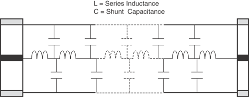
Transmission line theory is fundamentally about the transient response of a data path. As such, the theory attracts complex mathematical equations. A common problem in applied engineering is that practicalities become submerged in abstract mathematical models, which is often the case in transmission line theory. Sometimes it is worthwhile to stand back from the complex theory and consider the basic concepts of transmission line behavior that are in essence intuitive and straightforward. The first point to note is that the analysis of the signal traveling along the stripline, shown in Figure 3-4, concerns AC impedance. This is a first-order model of a transmission line, and we essentially ignore the DC characteristics of the stripline. Imagine a fast edge applied to the stripline shown in Figure 3-4. The time taken for the signal to travel along the line is the time taken for the signal to charge each capacitive section distributed along the line. Moreover, the signal attenuation depends on the line's AC impedance, which is proportional to the inductance and indirectly proportional to the capacitance. In other words, if the line's shunt capacitance increases, the stripline's impedance decreases. But if the series inductance increases, the line's impedance increases. What this means in practice is that if the line's capacitance increases, the signal travels more slowly down the line. If the inductance increases, the signal suffers a greater amount of attenuation.
Figure 3-4. Looking into a section of stripline to view the LC model seen by a transient signal.
A greater worry in SI engineering is the continuity of impedance in a transmission path and the effect that discontinuity has on digital signals. Consider a worse case, in which the signal-carrying conductor in the stripline shown in Figure 3-5 is unterminated. You can see that the incident signal climbs to twice its amplitude at the open end before reflecting along the line. This phenomenon of signal reflection at an open-ended line is obvious when you consider that the end of the line is an open circuit. Removing the line from the signal transmitter terminals would be the same as applying an open circuit to the transmitter. Therefore, it should come as no surprise that a line with no termination produces a reflected signal of twice the incident signal amplitude, similar to removing the load from the transmitter terminals. Likewise, a line with a short circuit produces a negative reflected voltage. This voltage subsequently cancels the incident signal and ultimately produces zero voltage at the transmitter terminals, as if they had a short circuit applied.
Figure 3-5. An intuitive image of a signal edge as it traverses and reflects at an open-ended stripline.
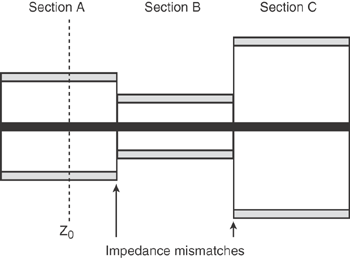
Dr. Eric Bogatin gives a splendid intuitive account of transmission line properties, along with detailed mathematical descriptions, including characteristic impedance, in his renowned book Signal Integrity Simplified. He shows that a line's impedance is inversely proportional to the square root of the capacitance per unit length of line and is directly proportional to the square root of the inductance per unit length of line. Figure 3-6 illustrates the relationship between transmission line impedance and capacitance. As it implies, the characteristic impedance of a transmission line is the line's instantaneous impedance as seen by the signal traversing the line, given as Z0 and measured in ohms. The characteristic impedance is dependent on a line's physical properties, such as the dielectric material that determines the inductance and capacitance per unit length of the line. But the characteristic impedance is unrelated to the actual length of the transmission line. As the dimensions of the transmission line change from the standard section A to the narrower section B, the line's capacitance increases, and therefore the line's characteristic impedance decreases. Likewise, as the transmission line section B in Figure 3-6 widens in section C, the capacitance decreases. Consequently, the line's characteristic impedance increases.
Figure 3-6. A length of stripline with three distinct characteristic impedances.
An intuitive way to think about transmission line theory is to remember that if excess inductance exists at one point in the transmission line, this causes a corresponding increase in the line's impedance at that point. Likewise, any excess in capacitance in the transmission line results in a corresponding decrease in the line's impedance. For example, capacitive loading is common in many via structures found in high-speed backplanes. Typically this causes the characteristic impedance of the transmission line to drop dramatically at the feed-through structure. Consequently, the possibility of an impedance discontinuity at a via and its effect on signal integrity is a significant concern in the successful design of high-speed systems. Therefore, we need to investigate further the effects of impedance mismatches in high-speed systems.
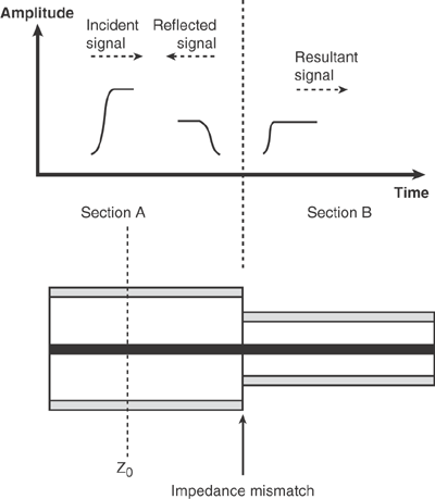
A digital signal traverses a transmission line as an electromagnetic wave. Any discontinuities in a line result in unwanted signal reflections. Reflected signals appear at transmission line discontinuities because there cannot be instantaneous changes in voltage or current at the discontinuities. The significance of a reflected signal is the effect it has on the incident signal, whereby the resultant signal is the phase and amplitude addition of the incident and reflected signals, as shown in Figure 3-7. Reflected signals can cause a range of unwanted SI manifestations, such as ringing. Ringing can lead to high-frequency signal components, resulting in unwanted electromagnetic radiation, crosstalk, and noisy return or ground currents. Ideally, the transmission line will have continuous characteristic impedance without discontinuities throughout its entire length, from transmission source to receiver termination.
Figure 3-7. The general effect that impedance discontinuities have on a digital signal traversing a line.
To summarize, we noted that a high-speed digital signal would see the transmitter, the PCB track with its interconnections, and the receiver as an entire transmission system. The communication system for a high-speed signal is often a complex arrangement, although many tools and techniques are available to make the design and verification of transmission line systems manageable. Moreover, you have seen that it is critical for the digital signal designer to have an intuitive understanding of basic transmission line theory to avoid signal integrity problems.
3.3. The Reflection Coefficient, Impedance, and TDR Concepts
TDR involves measuring and visualizing signal paths, interconnects, and terminations. TDR is a diverse measurement methodology with applications in optical, electronic, and mechanical systems. The significant feature of TDR is its ability to produce an image of a signal route, impedance, or communication path. The electric version of TDR enables the SI engineer to translate abstract models and signal propagation hypotheses into real-world observations of the physical layer structures within the interconnect path.
Visualizing the characteristics of a transmission line can be tricky. This is unlike in Roman times, when an engineer had little trouble visualizing the dimensions of his foot and the inch, which was more or less the thickness of his thumb. A key skill in designing or debugging a high-speed digital system is the SI engineer's perception of signal path parameters. TDR gives the SI engineer accurate knowledge of critical signal path characteristics. Moreover, TDR provides illustrative data that allows the engineer to determine if transmission environment parameters are within allowable limits.
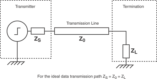
Figure 3-8 shows that the impedance of a signal source output (ZS), along with an associated transmission line impedance (Z0) and receiver impedance or load (ZL), which should correspond or match Z0. Signal reflections generated by unequal impedances are the enemy of good signal integrity. An important transmission line parameter measured by TDR is the ratio of the reflected signal to the incident signal, which is the reflection coefficient, given the symbol r (rho). The reason for the importance of the reflection coefficient in TDR is the direct relationship between reflection coefficients and impedance discontinuities. The principal purpose of a TDR instrument is to measure incident and reflected signals, calculate the reflection coefficients, and display the mathematically translated reflection coefficients as impedance or other relevant units.
Figure 3-8. The ideal transmission path.
Equation 3-2
![]()
If we plug numbers into Equation 3-2 to represent three classic conditions—a matched load, a short circuit, and an open load—we can see that r has a range of values from plus one (+1) to minus one (-1), with 0 representing a matched load:
• A matched load occurs when ZL is equal to Z0, and the load impedance and transmission line characteristic impedances match. This is the ideal case. The reflected wave, Vreflected, is equal to 0, and r is 0. There are no reflections.
Where there is zero reflected signal voltage:
![]()
• A short circuit occurs when the load impedance ZL is 0, which implies a short circuit. The reflected wave is equal to the incident wave, but opposite in polarity. The reflected wave negates part of the incident wave, and the reflection coefficient r is minus 1 (-1).
Where the reflected signal voltage equals the minus incident signal voltage:
![]()
• An open circuit load occurs when the load impedance ZL is infinite; an open circuit is implied. The reflected wave is equal to the incident wave and is of the same polarity. The reflected wave reinforces part of the incident wave, and the reflection coefficient r has a value of 1 (+1).
Where the reflected signal voltage equals the incident signal voltage:
![]()
TDR is in essence a simple measurement concept based on the determination of the reflection coefficient r. TDR instruments typically generate a very fast digital edge as an incident signal and measure reflected signals produced by the unit under test, as shown in Figure 3-9. Mathematical functions built into a TDR instrument compute r and fundamentally apply Equation 3-3 to determine the characteristic impedance (Z0) of the unit under test, as shown in Figure 3-9. It is important to note in Equation 3-3 that the accuracy of any TDR calculation of Z0 depends not only on measured signals but on the precision and accuracy of the known source impedance ZS.
Equation 3-3
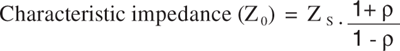
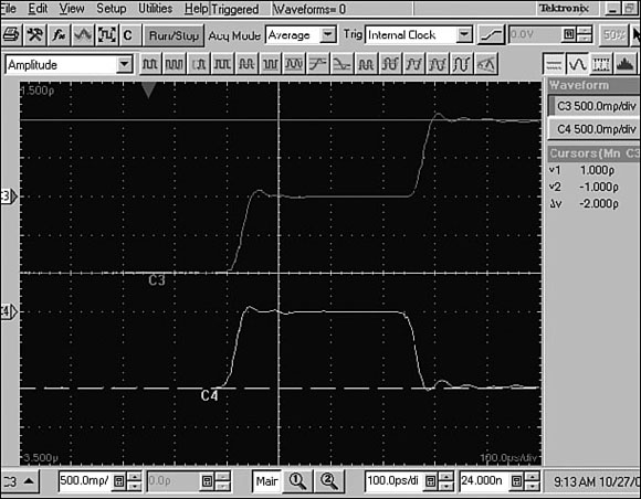
Figure 3-9. The oscillogram shows the time domain measurement of a step waveform passing through a short transmission line. The top waveform illustrates an open circuit line where the reflection coefficient r is +1. The bottom waveform shows a short circuit line where the reflection coefficient r is -1.
You will see that a key skill in designing or debugging high-speed digital systems is the ability to use TDR to visualize signal path parameters. So far, you have seen the need for the signal integrity engineer to have accurate knowledge of critical signal path characteristics. More importantly, the engineer often needs to know whether the parameters are within allowable limits.
3.3.1. TDR Concepts
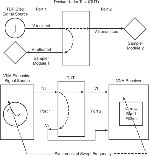
TDR measures the reflections that result from a signal traveling through a transmission environment of some kind—a circuit board trace, a cable, a connector, and so on. The instrument generates a known step with known source impedance (ZS) and rise time (Dr). Therefore, the initial signal launched into the device under test (DUT) is a known incident signal (VS), as shown in Figure 3-10. Normally the generated step signal has a programmable edge rate, where an edge rate of 35 picoseconds would provide excellent resolution of DUT impedances. To be able to resolve the very fast edge rates of the incident and reflected signals, the equivalent time sampler module typically requires a bandwidth on the order of 50 GHz.
Figure 3-10. A simplified block diagram of a TDR measurement system.
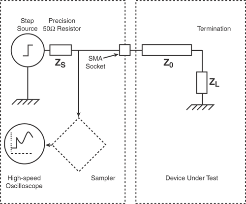
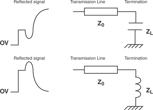
If the DUT has a characteristic impedance (Z0) and termination impedance (ZL) that match the source impedance (ZS), as shown in Figure 3-11, the signal seen by the sampler is half the amplitude of the generated pulse, given the step generator output impedance is also equal to ZS. The measurement circuit forms a simple potential divider network. In addition, the time taken for the reflected signal to return to the sampler is twice the propagation delay of the device under test. Fortunately, the engineer is unconcerned with the mechanics of TDR, because the instruments incorporate mathematical functions to allow the instrument to display actual device impedances and distance, or voltage against time. However, we must consider a few classic cases in which the DUT has common impedance discontinuities and the reflected signal can take a number of standard forms. An experienced TDR engineer generally recognizes a dip in a reflected signal as a shunt capacitance and a spike as a series inductance in the transmission path. The ability to read and decipher the TDR trace, relating trace figures to circuit elements, is valuable, as shown in Figures 3-12 and 3-13. A greater skill, however, is the ability to relate the effect that particular circuit discontinuities or features will have on transmitted data.
Figure 3-11. An ideal DUT with no reflected signals.
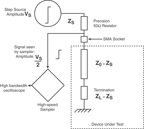
Figure 3-12. TDR trace illustrations showing common circuit discontinuities and their associated trace shape.
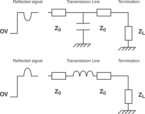
Figure 3-13. TDR trace illustrations showing common terminations and their associated trace shape.
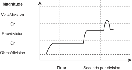
The TDR display is the voltage waveform that returns when a fast step signal propagates a transmission line. The resulting waveform seen by the sampler is the combination of the incident step and reflections generated when the step encounters impedance variations in the DUT. However, in a real DUT, multiple reflections are commonplace. Although TDR measurements are simple in concept, their real-word interpretation has complicated mathematical foundations. Most TDR instruments incorporate dedicated software to compute complex algorithms to resolve multiple images and produce numeric results displayed as clearly identifiable impedance waveforms. Additionally, most modern TDR instruments display magnitude measurements in units of volts, ohms, or r per division on the vertical scale and display units of time (seconds per division) on the horizontal axis, as shown in Figure 3-14.
Figure 3-14. A simplified illustration of a TDR waveform.
It is worth noting that to fully appreciate the TDR display, you need to keep in mind the characteristic reflection waveforms reproduced by idealized transmission line impedances. Moreover, as you have seen, you should be familiar with the effects of diverse transmission line impedances and terminations, such as capacitive and inductive loading.
3.4. Looking at Real-World Circuit Characteristics
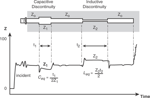
In general, etched circuit boards have impedance-controlled microstrip and stripline transmission lines. Over the span of these transmission lines, components, vias, connectors, and other "interruptions" create impedance discontinuities. Typically, a simulation model of these discontinuities centers on lumped inductors, capacitors, and transmission line losses. A real-world TDR trace of a prototyped DUT shows these discontinuities as a road map of the impedance variations. The waveform shown in Figure 3-15 is the result of a TDR step launched into a complex transmission medium.
Figure 3-15. The TDR waveform shows the effect of all the reflections created by all the impedance discontinuities in the DUT. The waveform is like a road map of the impedance variations in the DUT.
A TDR sampling module requires a very accurate, controlled pulse with a fast rise time and minimal aberrations. Imagine sending a typical data waveform down the transmission path shown in Figure 3-15. The data typically would have its own aberrations that would interact with the discontinuities in unpredictable ways. Such situations lend themselves to erratic, intermittent SI problems. Characterizing a transmission environment with TDR measurements and correcting impedance discontinuities can significantly improve signal integrity. However, to achieve accurate TDR measurements, it is important that the SI engineer appreciate the necessary requirements for an accurate incident pulse, precise reference impedance, and meticulous instrument calibration. Some TDR instruments have an architectural design that allows the automatic minimization of step aberrations to less than 4%. This function maintains high accuracy of the reflection coefficient and the resultant extracted impedance profile.
A high-performance TDR instrument provides attributes that allow intuitive test and measurement and a high level of confidence in the measurement accuracy. Some high-performance TDR instruments have a PC or workstation platform and host both the simulation tools and real-world measurements. A useful facet of high-performance TDR is the ability to compare real-world TDR measurements and simulated waveforms to determine how much impedance deviates from its required value and quickly rework the simulation. Reducing the development time is a prime aim of the SI engineer, who typically is under pressure to minimize a product's time to market.
3.5. TDR Resolution Factors
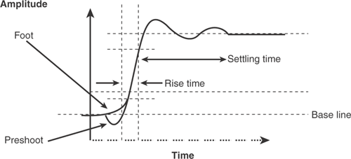
We have established that TDR measurements can produce useful insights into circuit impedance and signal integrity. However, not all TDR solutions and, in particular, TDR instruments are created equal. Several factors affect a TDR system's ability to resolve closely paced discontinuities. If a TDR system has insufficient resolution, small or closely spaced discontinuities typically merge or are smoothed together into a single aberration in the waveform. This effect may not only obscure some discontinuities, but it also may lead to inaccurate impedance readings. Rise time, settling time, and pulse aberrations can also significantly affect a TDR system's resolution. Many factors contribute to the accuracy of a TDR measurement. These include the TDR system's step response, interconnect reflections and DUT losses, step amplitude accuracy, baseline correction, and the accuracy of the reference or source impedance (ZS) used in the measurements.
A TDR system can only resolve two closely spaced discontinuities by half the rise time of the incident pulse, often quoted as the TDR resolution. However, realize that for a single discontinuity, the quoted TDR resolution is unimportant. A single discontinuity, such as a via, typically would be seen at a fifth of the TDR incident pulse rise time. Therefore, a TDR instrument with 35 picoseconds of rise time would have sufficient resolution to identify two discontinues spaced 0.1 inch apart on an FR4 PCB and show a single aberration where the feature size is in the region of 0.025 inch.
3.5.1. Rise Time
A reflection from an impedance discontinuity in a DUT has a rise time equal to or longer than (slower) that of the incident step. The physical spacing of any two discontinuities in the circuit determines how closely positioned their reflections will be relative to one another on the TDR waveform. Two neighboring discontinuities may be indistinguishable to the measurement instrument if the distance between them amounts to less than half the system rise time of the incident signal. Equation 3-4 summarizes this concept.
Equation 3-4
![]()
3.5.2. Pre-aberrations
Aberrations that occur before the main incident step can be particularly troublesome because they arrive at a discontinuity and begin generating reflections before the main step arrives. These early reflections reduce the resolution of the TDR measurement by obscuring closely spaced discontinuities.
3.5.3. Settling Aberrations
Aberrations, such as ringing, that occur after the incident step, as shown in Figure 3-16, cause corresponding aberrations in the reflections. These aberrations are difficult to distinguish from the reflections caused by discontinuities in the DUT. Note that aberrations in the TDR instrument's step generator and aberrations in the step response of its sampler have virtually the same effect.
Figure 3-16. A simplified diagram of a TDR generated pulse that contains signal aberrations.
3.5.4. Reference Impedance
All TDR measurements are relative. In essence they are direct comparisons between incident and reflected signal amplitudes. Modern TDR instruments perform all the associated calculations and show results directly in rho or ohms. However, apart from a comparison of incident and reflected voltages, Equation 3-3 confirms that the TDR process is notably dependent on the accuracy of the reference or source impedance (ZS). High-performance TDR instruments use high-precision 3.5 mm air line connectors as stable impedance references to calculate rho and ohms. Alternatively, proprietary 50-ohm standard connectors are specifically designed for the standard calibration of a TDR instrument.
3.5.5. Step Amplitude and Baseline Correction
In general, modern TDR instruments provide built-in calibration of the incident step amplitude and baseline level for accurate computation of test impedances. Moreover, high-performance TDR instruments place a known air line, or standard 50-ohm component, in the sampling module specifically for calibration purposes. This lets the instrument automatically and periodically monitor the baseline and incident step amplitude. Consequently, the system automatically compensates step amplitude and offset drifts, ensuring precise, repeatable measurements.
3.5.6. Incident Step Aberrations
The most obvious problem caused by incident step aberrations, such as a long setting time, is the inability to measure accurately reflected step amplitudes. When test impedances are significantly different from 50 ohms, reflections typically are of relatively low amplitude. TDR measurement accuracy is highly dependent on the precise measurement of the reflected signal amplitude. If test impedances notably differ from 50 ohms and the incident pulse fails to settle in a relatively short time, in comparison to the propagation delay of the line under test, serious measurement errors will result. The closer the DUT impedance is to 50 ohms, the greater the accuracy of the measurement system and, in particular, the higher the measurement system's tolerance to incident step (settling time) aberrations.
A second type of aberration that can cause problems is the foot or pre-shoot that precedes the incident step. If the transmission line under test has an open circuit termination, the step's foot or pre-shoot generates reflections at the open circuit. These reflections appear before the step's reflected rising edge comes into view. This second type of step aberration causes obvious, unwanted end-of-line measurement errors. However, low-frequency step aberrations cause a more subtle effect.
Low-frequency incident step aberrations can appear as a slope in the TDR trace, which is an instrument-generated artifact. Such an artifact can even appear when an external calibration 50-ohm termination replaces the DUT. In effect, a low-frequency aberration in an incident step function can cause the TDR instrument to display an erroneous offset measurement.
3.5.7. Noise
Random noise can be a significant source of error when making TDR measurements, particularly when measuring small impedance variations. Fortunately, modern instruments can perform signal averaging to reduce the effects of random noise. The drawback in many instruments is that averaging can dramatically slow the processing speed, particularly when displaying automatic measurements. Modern high-performance oscilloscopes, which form part of a TDR measurement system, addresses this problem with built-in multiple processors that can share the processing workload and produce real-time denoised measurements.
3.5.8. Interconnect Accuracy and Reflections
TDR measurements that require a long probe cable are prone to measurement inaccuracies. To reduce the effect of the cable loss in a long probe cable, it is wise to measure the DUT relative to the end of the probe cable. The rho of the probe cable (r cable) causes a shift in the reference level of the TDR measurement. The incident step amplitude presented to the DUT will be 1 minus the rho of the cable (1 – [r cable]). Consequently, for maximum accuracy, the SI engineer has to measure the probe cable rho and use a measurement technique that compensates for losses in the probe cable. Moreover, reflections from poorly designed interconnect components and unsatisfactory probe-to-DUT interfaces cause TDR measurement problems.
Therefore, it is worth noting that an unsatisfactory TDR probe interface can create a large inductive reflection, and the reflected signal must settle before you can make an accurate measurement. To minimize measurement errors, it is extremely important to keep the TDR instrument's probe tip and ground leads as short as possible. This reduces the ground loop inductance and creates a good launch point for the TDR step.
3.5.9. Cable Losses
Cable losses in the test setup can cause several problems. Both conductor loss and dielectric loss can occur, but conductor loss usually dominates. Conductor loss results from the finite resistance of the metal conductors in the cable. Due to the skin effect, the resistance increases with frequency. The result of this incremental series resistance is an apparent increase in impedance, as you look further into the cable. Therefore, with long test cables, the DUT impedance looks higher than it actually is.
The second problem is that by the time an incident pulse reaches the end of a long probe cable, both the rise and settling times are degraded. Degradation in the incident pulse can severely affect TDR measurement resolution and accuracy, because the effective amplitude of the incident step differs from the expected calibrated value. Fortunately, incident pulse amplitude inaccuracy does not cause a serious error when the DUT impedance is close to 50 ohms. But for DUT impedances that are noticeably larger or smaller than 50 ohms, the measurement error can be significant.
3.5.10. Controlling Rise Time
Although in many cases the fastest available incident step rise time is desirable, in other cases very fast rise times can give misleading results on a TDR measurement. In essence, it is unnecessary to overdesign a board by finding and correcting impedance discontinuities that will be invisible to the real-world or applied signal. For example, testing the impedance of a microstrip on a circuit board with a 35 picosecond rise time system provides excellent resolution. Reflections from small discontinuities such as stubs or sharp corners in the microstrip are quite visible when excited by the TDR step. However, if the same transmission line were to convey a 10 Gbps signal, a higher-resolution TDR signal would be appropriate for the board's test and characterization.
This difference between measurement and reality could be the beginning of a signal integrity problem. In attempting to correct the misleading impedance readings, you might compromise the environment that the real operational signals need. It is often preferable to see the transmission line's TDR response to rise times, similar to the actual circuit operation. Some TDR instruments provide a means of increasing the apparent rise time of the incident step. Moreover, some high-performance sampling oscilloscopes implement filtering using a double-boxcar averaging technique that is equivalent to convolving the waveform with a triangular pulse. Fast filtering using live waveform mathematics shows the filtered response in near-real time. This technique provides live filtered waveforms that quickly respond to changes, and it requires no additional calibration steps. The alternative measurement method is to use an external pulse generator, although the high-performance TDR instrument filtered waveform result corresponds very well with similar measurements made with an equivalent pulse from an external generator.
High-bandwidth TDR sampling heads are extremely static-sensitive. To ensure their continued performance in impedance and signal integrity applications, they require a high level of static protection. This is beyond the simple protection that suffices for conventional oscilloscopes. The following guidelines are essential when handling or using any high-bandwidth TDR sampling module:
• Cap or terminate probes and sampling inputs when not in use.
• Use grounded wrist straps of less than 10 megohms when in contact with the TDR probes and sampling module.
• To prevent the possibility of probing a device that may have built up a charge, always discharge the device before probing or connecting it to the module. You can do this by touching the device with the probe ground lead or your finger—assuming you are using a wrist strap—to the point you want to TDR test. Some high-performance instrument manufacturers, such as Tektronix, provide a static isolation unit that uses a microwave relay to isolate and automatically discharge the DUT. With this unit, the DUT cable remains connected to ground until a foot switch is depressed and the relay switches, connecting the DUT to the TDR input.
• Remember that long cables stored in a draw can build up a static charge over time. They must be grounded before being connected to the TDR instrument.
3.6. Differential TDR Measurements
Differential transmission lines offer many advantages over conventional transmission channels. Many high-performance designs, such as high-speed serial buses, use differential impedance or balanced lines to minimize SI issues. Although differential signaling offers many advantages, there remains a need to make differential TDR measurements to support signal integrity. All the single-ended TDR measurement concepts discussed so far also apply to differential transmission lines. However, the basic principles of TDR require additional measurement concepts and instrumentation techniques to take into account the unique requirements of measuring differential impedance. The additional instrumentation hardware requirement is a four-channel TDR or four-port VNA.
A differential transmission line has two unique modes of propagation, each with its own characteristic impedance and propagation velocity. Much of the literature calls these the odd mode impedance and the even mode impedance:
• A definition of odd mode impedance is the impedance measured by observing one line referenced to ground while driving the other line by a complementary signal.
• The differential impedance is the impedance measured across the two lines with the pair driven differentially. Differential impedance is twice the odd mode impedance.
• A definition of even mode impedance is the impedance measured by observing one line referenced to ground while driving the other line with an equivalent signal.
• The common mode impedance is the impedance of the lines connected in parallel, which is half the even mode impedance.
Tying together the two conductors in a differential line and driving them with a traditional single-ended TDR system yields a good measure of common mode impedance. However, common mode impedance is often less important than the differential impedance. To provide true differential impedance measurements, the TDR sampling module needs to provide a polarity-selectable TDR step for each of two channels. This approach drives the differential system under test in true differential mode, just as it does when the DUT is functioning in its intended application. Moreover, separate responses, acquisitions, and evaluations of the differential line provide true TDR measurements of the differential line. Alternatively, a mathematical calculation based on linear supposition is used to correct the resultant reflections produced by exciting the differential circuit with staggered step inputs. This mathematical function built into some TDR instruments provides an accurate analysis of most differential circuits.
However, to achieve a real-time differential TDR measurement, both sampler channels must have a matched step response. Also, the two incident steps must be matched but complementary, and the incident steps must be time-aligned at the DUT. To meet these requirements, the TDR instrument typically incorporates two acquisition and polarity-selectable TDR channels in a single sampling module containing a common clock source. Moreover, the relative timing of the two-step generators should be deskewed to precisely align the two incident steps at the DUT and remove any mismatch due to cabling.
With the TDR system set up with complementary incident steps, and using ohm units, adding the two channels yields the differential impedance. The individual traces give the odd mode impedance. If the line is not balanced, the two traces do not match exactly.
3.6.1. Deskewing the Step Generators
Differential TDR measurements require precise matching of both the stimulus and the acquisition systems in terms of timing and step response. The TDR instrument fixes the timing of each incident step response; however, the relative timing of the two channels is usually adjustable. Both the acquisition timing and the TDR step timing must match to yield a valid TDR measurement. Notice, however, that the matching requirement lies at the DUT rather than the front panel of the instrument. Poor matching between the cables or interconnect devices and the DUT skews the TDR incident steps in time when they arrive at the DUT, even if they are aligned at the instrument's front panel. This causes significant measurement error.
The most efficient way to eliminate or reduce measurement skewing is to minimize the DUT interconnect lead length and to use carefully matched probe cables. Extending the sampling head 2 meters from the mainframe is possible in some high-performance TDR instruments and incurs no loss in performance. This helps minimize probe cable lengths with associated mismatch, loss, dispersion, and other interface errors. Deskewing the acquisition paths is very important. In some instruments the timing of the step generators and acquisition can be difficult to detect and correct. Individually adjusting the incident steps and setting the acquisition is not always obvious. However, a number of high-performance instruments provide a specific trace that shows the effect of a timing mismatch in real time. Displaying the effects of a mismatch in real time makes the adjustment of the instrument simple and intuitive.
3.7. Frequency Domain Measurements for SI Applications
The two principal measurement techniques for passive signal integrity characterization of data path transmission and modern digital system gigabit interconnects are time domain TDR and frequency domain VNA. Differential transmission lines coupled with the microwave effects of high-speed data have created the need for the VNA and characterization of physical layer components. There is often a need to test and characterize complex microwave behavior in bound conductors with a frequency measurement, such as a high-speed digital interconnect. In fact, many digital standards groups recognize the importance of specifying frequency domain physical layer measurements as a compliance requirement.
Nonetheless, as you have seen, the TDR instrument is a very wide bandwidth equivalent sampling oscilloscope with an internal step generator. The TDR sends a step stimulus to the DUT. Based on reflections from the DUT, the designer can deduce a lot of information about the device properties, such as the location of failures, impedance, and time delay information. TDR allows the engineer to gain insight into the DUT's topology. With the aid of built-in mathematical functions and an additional sampling channel, or module, the TDA instrument makes possible Time Domain Transmission (TDT) measurement, as shown in the top part of Figure 3-17. TDT measures crosstalk or characterizes lossy transmission line parameters, such as rise time degradation, return loss, and skin effect and dielectric loss. However, a TDT measurement system requires a high-performance TDR with an additional sampling channel, as well as comprehensive dedicated software to translate time domain measurements into DUT frequency-dependent behavior. VNA instruments work in the frequency domain and are altogether different in concept from time domain TDR tools. VNA instruments apply sinusoidal waves as a signal source to stimulate the DUT. They use a very narrow band filter at the receiver to determine the device's response. Moreover, because of the narrow bandwidth receiver inside the VNA, the VNA's resultant noise floor is inherently lower than a TDR instrument. By sweeping the signal source and the receiver's filter in a synchronized fashion, the VNA instrument makes a swept-frequency, steady-state measurement, as shown in the bottom part of Figure 3-17.
Figure 3-17. Simplified block diagrams of two-port networks where the signals at the input and output terminals characterize the frequency domain scatter measurements or S-parameters.
A frequency domain VNA measurement separates and measures scattered signal amplitudes and phase produced at a two-port network. A VNA instrument uses built-in mathematical functions to translate scatter measurements into S-parameters, which are ratios of incident wave voltages to reflected or transmitted wave voltages for a two-port measurement. The VNA instrument can display S-parameters as signal power against frequency, frequency magnitude and phase, or graphically on a Smith chart. The DUT is effectively a black box where the applied signals, reflected signals, and resultant output signals determine the behavior and frequency domain S-parameters of the complete component or DUT. The ratio of the Vincident and Vreflected signals gives the S11 and S21 parameters, called the reflection and transmission coefficients. To some extent they are similar to reflection and transmission coefficients in a time domain measurement.
The fundamental difference between the TDR and VNA instruments is that the TDR measures voltage against time, and the VNA measures power against frequency. The displayed measurements are quite different. Moreover, there is a fundamental difference in that VNA measurements relate to the frequency characteristics of a DUT in total, whereas TDR measurements give information about each discrete discontinuity in a transmission path. Nevertheless, we know from basic signal transformation theory that the Fourier transform relates the time and frequency domains. The time and frequency domains show the same information in different forms. Each domain contains the same information, but in a different representation. Moreover, there are clear relationships between TDR reflection and transmission coefficients and VNA S-parameters. These relationships allow dedicated software in a TDR system or VNA instrument to show both frequency and time domain information. The preferred representation is the prerogative of the engineer. In general, the RF or microwave engineer prefers the frequency domain. Digital design engineers live in the time domain, where they are most at ease with their time-related measurement environment. However, the advent of special signal integrity software to control both TDR and VNA instruments has created a new generation of engineers who use both time and frequency domain analysis.
TDR is visual and intuitive due to the transient nature of the measurement technique. The incident step propagates through the discontinuities in the DUT, and the reflections indicate the exact location and size of discontinuities. The fast TDR rise time of 35 ps ensures that the time domain is a broadband measurement that captures a wide range of frequencies. This allows specialist software to translate TDR measurements into frequency domain S-parameters.
However, a dedicated VNA instrument has a better frequency domain performance than an equivalent TDR instrument and therefore greater accuracy in characterizing some high-frequency signal paths. However, it comes at a price, because the dedicated VNA instrument is more expensive compared to a TDR-based system. When choosing an instrument, it is important to consider the cost-benefit ratio of a VNA instrument. An equivalent TDR instrument does not provide the same frequency domain performance as a VNA. It is up to the digital design engineer to decide whether the parameters within their system justify the extra performance and cost of a dedicated VNA instrument.
The dynamic range of VNA measurements tends to be substantially higher than that for TDR measurements. Typically a VNA instrument has a 110 dB dynamic measurement range, compared with 50 to 60 dB for an equivalent TDR instrument. Originally, the development of VNA instruments centered on microwave design. Engineers were concerned primarily with narrowband and resonant systems, such as mixers, filters, resonators, power splitters, and combiners. Microwave engineers required exact data about the frequency band over which a circuit could operate, its center frequency, and its Q-factor. These requirements caused instrument manufacturers to continuously improve VNA accuracy and achieve very high dynamic range, wide signal-to-noise ratio, in the frequency domain. Today a high-performance VNA instrument easily exceeds 100 dB when careful measurement techniques are used. To achieve this high dynamic range and accuracy, a narrowband filter analyzes data at each frequency point. The alternative would be to use a TDR and, where necessary, use dedicated software to translate the time domain measurements into frequency domain S-parameters. However, the high dynamic range in a VNA makes a significant difference to the measurement of transmission lines that exhibit microwave properties.
A high-performance sampling oscilloscope TDR system with an incident pulse of 35 ps rise time typically allows the digital design engineer to measure up to 12 GHz of S-parameters, with up to –60 dB of dynamic range. With the addition of dedicated software, the fast rise time TDR enables the engineer to perform S-parameter measurements up to 65 GHz, with up to –70 dB of dynamic range. Nonetheless, a VNA offers a significantly improved measurement performance in the microwave frequency bands. Moreover, the engineer often prefers to work in the time domain and to translate results into the frequency or to work purely in the frequency domain.
The similarities and differences between TDR and VNA allow the two instruments be applied to different aspects of gigabit interconnect modeling. With the addition of specialist software, the designer can use either instrument to generate gigabit interconnect SPICE or IBIS models and to analyze eye diagrams, jitter, losses, crosstalk, reflections, and ringing in PCBs, device packages, sockets, connectors, and cable assemblies. Time domain-based analysis provides the designer with topological interconnect models, which have one-to-one correlation between the model components and the physical interconnect structure. Such models can include frequency-dependent losses and resonances. They are most convenient for troubleshooting where they enable the SI engineer to identify causes of signal integrity problems, within required time scales and budget.
Conclusion
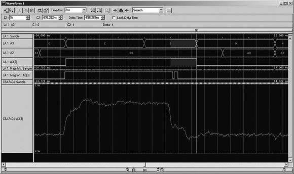
High data rates of 10 Gbps and above are particularly sensitive to mismatches and variations in transmission path impedance—especially resultant signal reflections that significantly decrease signal quality. The integrated oscilloscope and logic analyzer display shown in Figure 3-18 shows the classic effect that reflected signals have on the edges of a digital signal. The signal edges appear to have a midpoint step or a gnawed edge, as if bitten. These particular effects were produced by an incorrectly terminated PCB track.
Figure 3-18. The detrimental effect a reflected signal has on the edges of a digital signal.
Impedance tolerances are part of the electrical specifications for many of today's high-speed buses and digital system components. While it is standard practice to model high-speed circuits where modeling hastens the design cycle and minimizes errors, there remains a need to prototype a modeled design to verify its parameters with hardware measurements. Moreover, calculating or modeling the time domain response of a section of printed circuit board track from first principles typically involves an intimate knowledge of electromagnetic field theory, such as the solution of Maxwell's equations. Electromagnetic theory is all-inclusive and typically takes into account all the electrical parameters and device geometry of a particular electronic component or connection system. Although microwave engineers and device manufactures have traditionally used specialist electromagnetic toolsets to model connectors and transmission lines, digital engineers generally have only working knowledge or an appreciation of electromagnetic field theory. Today, electromagnetic field theory is not a core subject for the majority of digital engineers. Nonetheless, this is a high-speed digital world. The digital design engineer needs to understand the high-speed signal transmission environment, analyze impedances in the time domain, and characterize signal channels in the frequency domain. You have seen that TDR is inherently an intuitive measurement system. Used wisely, it should enable the SI engineer to design and produce reliable high-performance digital systems. Understandably, there is a limitation to the depth and detail that we can give to signal path analysis. One of the victims is the scope given to S-parameters and frequency domain measurements. In essence, this chapter has attempted to describe the fundamental principles of TDR and make you aware of VNA. Even so, many other facets of TDR and VNA remained unexplored in this chapter. Our hope is that you have a firm understanding of TDA and an awareness of VNA. We also hope you're inspired enough to investigate further the applications of TDA and VNA in the myriad of white papers and trade articles.