14
Final Statements
14.1 Introduction
The book has outlined many of the techniques needed to create FPGA solutions for DSP systems. Some of these have been encapsulated within the design tools and then applied to a number of design examples. In addition to achieving efficient FPGA implementations in terms of area, speed and throughput rates, the book has also covered the key area of low-power implementations, briefly covering a number of techniques to reduce the dynamic power consumption. The key of these approaches was to derive an efficient circuit architecture which successfully utilized the underlying resources of the FPGA to best match the computational and communication requirements of the applications. Typically, this involved using high levels of parallelism and pipelining.
If FPGA-based DSP system implementation is to be successfully automated, this requires incorporation of the tools described in Chapter 9, either within commerical HDL-based or C-based design tools (as is beginning to happen with the Synplify DSP tools), or within higher-level design environments such as those outlined in Chapter 11. If this is to be successful, then any high-level approach should allow designers to create efficient FPGA implementations from high-level descriptions, and/or to incorporate existing IP cores, as this may represent considerable years of design time, within the high-level design flow.
The purpose of this chapter is to give some attention to issues which have either had to be ignored or that have not been described in detail. In Section 14.2, reconfigurable FPGA systems fall into this latter category, as the underlying programmable nature of FPGAs provides an interesting platform to allow the realization of such systems. Two topics which need additional comment and which are mentioned in the text in Sections 14.2 and 14.3, are implementation of dedicated floating-point hardware on FPGA and the creation of memory architectures, respectively. In Section 14.4, the chapter also attempts to address future trends and outline future challenge for FPGA developers.
14.2 Reconfigurable Systems
Conventionally, the realm of programmability has been the domain of the microprocessor which executes a sequence of instructions describing the required behaviour of the system; system functionality is then changed by changing the instructions. This has the advantage that it does not require any modification of the circuitry, but is limited in that it cannot deliver the same processing performance and power consumption that comes with a custom hardware solution. The problem is that quite a considerable portion of the circuitry that goes into a modern microprocessor is used for storage and control. This overhead is needed to allow the computational tasks to heavily reuse the small, active portion of the microprocessor, namely the function units (FUs).
Conceptually, the FUs are all that are needed to evaluate the operations describing the system. However, in practice, a processor needs to move data between the FUs as well as between the memory and FUs. This is complicated by the practical limitation of how much fast multi-port memory can be placed near the FUs. To address this problem, the memory in a processor is organized into layers of hierarchy. The fastest, most costly memory (the register file) forms the top layer of the memory hierarchy and is placed at the heart of the system to store for values over multiple cycles. With each step down the hierarchy, the memory increases in capacity, but at the cost of slower access speeds. The movement and management of moving data between the layers is another essential task required of the processor.
The result of developing this programmable architecture is that a lot of transistors are not performing any useful computation at one time. In an environment where silicon area is increasingly becoming a premium commodity, there is a strong need to reduce the pressure on large memory blocks as this will lead to bottlenecks. With regard to system memory, there is an effect known as memory wall, as proposed by Flynn et al. (1989) which indicates that the ratio of the memory access time to the processor cycle time will increase as the technology improves.
This would tend to indicate that a major change is needed in terms of how architectural solutions are derived. To some extent this was seen in the 1980s where damning forecasts on the impact of interconnect delay implied a shift to new architectures, such as those based on systolic arrays architectures (Kung and Leiserson 1979, Kung 1988); one major development was the ill-fated iWarp multiprocessing supercomputer developed jointly by Intel and H T Kung's group at Carnegie Mellon University. The aim was to build an entire parallel-computing node in a single microprocessor with the classical organization of systolic arrays, namely with localized memory and nearest-neighbour communications links. Whilst this concept worked well for highly computational operations, such as matrix–matrix and matrix–vector-based computations, it worked less well for less regularly organized computations.
Reconfigurable computing however, does not suffer from this limitation as the main attraction is to change the hardware based on the computational needs. It is targeted at complex systems with the aim to organize functionality in such a way that the computationally complex aspects are decomposed into the field-programmable hardware; reconfigurable computing allows the acceleration seen in the earlier sections of this book to be achieved with the more control-orientated aspects being mapped to a more suitable platform, namely a processor. This infers the use of programmable processors connected to single or arrays of FPGAs.
14.2.1 Relevance of FPGA Programmability
In the early days of FPGAs, a number of different programming technologies emerged specifically E2PROM technology, antifuse technology and of course, SRAM technology. SRAM programming technology brought about an interesting mode of operation, namely that the functionality could be changed as part of the normal mode of operation or in other words, reconfigured. This could either be done statically between downtimes in normal modes of operation or dynamically, i.e. as part of the normal mode of operation. Basically, the FPGA comprise a huge amount of programmable logic, registers, memory blocks and dedicated processing blocks which can be configured to work in different ways to realize a variety of functions. The FPGA can be considered to be like a smart memory device where the ‘state’ of the structure is downloaded from a processor to the FPGA device. This configuration of the FPGA is then used to perform an operation on the incoming data. By rewriting different data to the FPGA device, the function performed on the data is changed. So, rather than writing and reading data to a memory device, we are storing data to the FPGA device which changes the function of the data fed into, and accepted back from, the FPGA device.
This is designated as comprising two distinct strata by (Maxfield 2004), namely the logic stratum which performs the operation as outlined above and stores the necessary information for the data in the available memories and the SRAM configuration stratum which contains the necessary programming information. Thus, interacting with the logic stratum is a normal mode of operation whereas programming the SRAM configuration stratum defines the mode of configuration. To use this as a programming mode is highly attractive, meaning it is possible to program the hardware to best meet the computational requirements under consideration, ideally on demand, as and when required.
This concept remains a key attraction as it meant that the available hardware resource could be configured to most efficiently implement the functionality required, but this presents a number of challenges. These include the impact of the time to reconfigure the hardware in environments such as DSP, where data is continually being fed and thus must be stored. In addition, there is the impact in processing time, as indicated by the graph in Figure 14.1 taken from Heron et al. (2001) which shows that the reconfiguration time TR can have an impact on the performance capability, even though the performance rate of the FPGA is superior. Thus there is a break-even time, TB after which it becomes advantageous to perform reconfiguration. The underlying reliability of a system is not in question as the state of the device is constantly being changed; the question must be asked if the hardware has configured properly.
14.2.2 Existing Reconfigurable Computing
There has been a lot of work on reconfigurable computing platforms, with a good reviews available (Bondalapati and Prasanna 2002, Compton and Hauck 2002, Todman et al. 2005). The classification of reconfigurable systems was highlighted initially in (Compton and Hauck 2002) and revised in Todman et al. (2005). A simplified version of the diagram shown in Todman et al. (2005) is given in Figure 14.2. The figure shows how reconfigurable units, typically in the form of FPGAs, can be added to conventional CPUs to provide the CPU/FPGA configuration.
In the first class shown in Figure 14.2(a), the reconfigurable unit is seen as an external processing unit. A number of example boards exist for this type of configuration from both main FPGA vendors, and also companies such as Celoxica. The second and third classes use a reconfigurable unit as a dedicated co-processor unit, either connected solely to the bus or to both the CPU and the bus. Research examples include RAPid (Ebeling et al. 1996) and Piperench (Laufer et al. 1999). The fourth class incorporates the reconfigurable unit or fabric within the CPU. This would either be in the form of a fabric to change the interconnectivity of the individual processor or could involve the reconfiguration of a subunit to change its functionality or individual interconnectivity, or both. An example is the reconfigurable algorithm processing (RAP) technology from Elixent (2005).
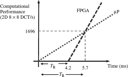
Figure 14.1 Impact of reconfiguration time for an 8 × 8 2D DCT implementation

Figure 14.2 Classes of reconfigurable systems
This comparison now is a little dated as the evolution in FPGA technology, as described in Chapter 5, indicates. FPGAs are now available with both software and hard microprocessors included on the FPGA substrate. This means that the concept of using FPGAs as a hardware accelerator can still exist, as demonstrated in some commercial and high-performance computing solutions, but now the concept of incorporating the core within the FPGA fabric exists. However, many of the issues addressed by the models still apply as many of the approaches considered the implications in terms of performance with regard to the ratio of communications/computing hardware, both in terms of speed and cost.
14.2.3 Realization of Reconfiguration
There are a number of ways that this reprogrammability can be realized where each approach has subtle, but important differences. The first lies in how the reprogrammability is used in the design to allow a degree of flexibility to be incorporated into the circuit. A large circuit will quickly become very large if many partially redundant components are incorporated at any particular instant of time. MacBeth and Lysaght (2001) highlight the unnecessary overhead of having a reprogrammable core in a reprogrammable device and propose categorizing these circuits as programmable multifunction cores (PMCs). This can also help FPGA realization close the performance gap with ASICs; in ASICs, circuits have to be developed in such a way that they provide versatility, allowing all possible situations to be covered in the one implementation, thereby trading area and speed for flexibility. As the FPGA fabric has to support reconfiguration by its very nature, these resources could be used to change the circuit (its state) so that the best circuit implementation can operate at any given time. The more tailored the circuit becomes, the more likely it will have to be modified to maintain the advantage, but there is a great benefit in terms of both circuit area and data throughput. Using the fabric of the FPGA as part of the process of changing the circuit's state, can deliver an area decrease of 21% and a speed increase of 14% (MacBeth and Lysaght 2001).
Run-Time Reconfiguration
FPGAs have a limited capacity to perform logic operations, but reconfiguration can be used to get around this. By time-sharing the FPGAs logic, the FPGA can implement circuit operations that are beyond the area capability of the hardware (Lysaght and Stockwood 1996). This has led to the concept of virtual hardware (Brebner 1999) where the physical resource does not limit the amount of circuitry that can be accommodated on a single device.
Run-time Reconfiguration (RTR) can be used to simplify the design of the hardware (Brebner 1999, MacBeth and Lysaght 2001, Walke et al. 2000). When a circuit design is constrained by being used across multiple tasks or by being reduced in size through data folding, it will cause complex timing issues and may require hardware sharing. Within the FPGA, a circuit can timeshare portions of the hardware. This can be used to simplify the circuit designs. For example, in a hypothetical system proposed by (Walke et al. 2000), three finite impulse response (FIR) poly-phase filters are required with different tap lengths; each filter was designed to time-share a limited number of multipliers, but not all at the same time; reconfiguring the circuitry with the choice of FIR filter to be used, removes the time and control complexity required to combine the three filters together. So when the hardware is required to cover a number of possibilities, for reasons of limited hardware resource or multiple standards, a system can reconfigure to select the parts of the circuit that are required. This has distinct advantages as it obviates the need to develop the complex control circuitry needed to switch the various circuit modes, such as that required in ASIC design.
14.2.4 Reconfiguration Models
A number of models have emerged for reconfiguration.
Single Context
The traditional model of the commercially available FPGA is the single context, which only allows the circuitry to be changed by loading a completely new configuration. This type of model is not best suited for RTR because of the associated time to make changes in the firmware. The speed at which the data can be written is limited by the bandwidth of the configuration data transfer from its source to the FPGA. This can be determined by the width (pins) and speed of the interface on the device and in the way it is interfaced to the system. While reconfiguration data is being written onto the device, the current circuitry cannot be used. Other features have been proposed and added to overcome this bandwidth limitation.
Partially Reconfigurable
Examples of commercial partially reconfigurable FPGAs include the Stratix®III family from Altera and the Virtex™-5 FPGA family from Xilinx. These devices have much more scope for RTR than single context FPGA as sections can be changed independently. As the reconfiguration sections are made smaller, the cost incurred in making changes to the circuitry reduces, thus allowing frequent changes without significant overheads. A feature that is often available with this type of device is reconfiguration with continued operation. While parts of the FPGA are reconfigured, other parts can still be functional, masking the time needed for reconfiguration.
Multi-Context
There have been a number of studies into multi-context designs (DeHon 1996, Scalera and Vazquez 1998, Trimberger et al. 1997), but so far this has not resulted in a commercially available product. These devices tackle the problem of transferring the reconfiguration data by storing more than one plane of reconfiguration data on-chip. The process of reconfiguration is achieved by selecting one of the planes to drive the configuration of the logic. The switch between contexts can be achieved in only a few clock cycles. The multiple contexts allow background loading of the configuration data, as the configuration data can be loaded into a context that is not active.
A possible problem with such a device lies in the number of contexts required in a typical system implementation, this may be greater than the available hardware and the sharing of data between contexts. The SCORE (Section 2.6.2) architecture shares some similarities with the multiplier contexts FPGA, but allows the amount of resources used for the contexts to be altered.
Pipeline Reconfiguration
The pipeline reconfiguration model views the reconfiguration of the device as pipelined blocks and can be seen as a modification of partially reconfigurable FPGAs (Luk et al. 1997). It is viewed as pipeline datapaths, each stage of which is reconfigured as a whole. This permits the overlapping of the reconfiguration and execution. The required reconfiguration is broken into stages of reconfiguration where each stage is loaded in sequence. After each stage has been programmed, it immediately begins to operate, thereby the configuration of a stage is exactly one step ahead of the dataflow. Once the device has run out of space, it starts to swap out stages that have been resident longest on the FPGA, replacing them in the next stage. This allows applications to exceed the physical resources of the device and still run with a reduced throughput. Piperench (Laufer et al. 1999) is an example of this type of model. In this case, the author points out the advantage of forward compatibility, as further devices can retain the same stages and just increase the numbers of stages.
Configuration Caching
Figure 14.3 shows an abstracted model of the FPGA, where there is a FPGA array and a reconfiguration data storage device. As it is not possible to supply the bandwidths required, the movement of configuration data can result in a long halt in the circuit processing. In this case, pre-fetching and caching can be used (Hauck et al. 1999), as shown in Figure 14.3, to reduce the ‘burstiness’ of the data movement. Caching data close to the FPGA's array, such as on-chip, makes it possible to use a high-bandwidth channel with the cache being fed via a narrow channel. However, a problem with pre-fetching occurs with conditional branching when incorrect data is fetched (Hauck et al. 1999).
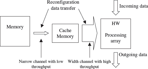
Figure 14.3 Pre-fetching and caching used to get around the bandwidth limitation of reconfiguration data transfer
Configuration Compression
Configuration compression reduces the amount of data to be moved and therefore cuts the reconfiguration time by using data compression. Figure 14.4 shows an abstract view of this model. As with the pre-fetching, the link from the decompression hardware to the FPGA array is much larger than the link to the reconfiguration data store. The concept was initially developed for the Xilinx XC6200 FPGA technology which has a wildcarding feature that allows address and data values to be written simultaneously to multiple locations. This device had been developed specifically to support dynamic reconfiguration and it recognized that it is necessary to change parts of the device at the same time, hence the wildcarding features. Hauck et al. (1999) showed that it is possible to compress the data streams in a way that allows the wildcarding hardware of the XC6200 to decompress the reconfiguration data stream. Hauck et al. (1999) and Li and Hauck (2001) went on to consider other compression methods with low overheads that can be used with other FPGAs.
14.3 Memory Architectures
The support for parallel and pipelining operation was highlighted as the major attraction of FPGAs when considered for implementing DSP systems. However, one factor that has received some attention throughout is the availabilitiy of a wide range of different sizes of parallel memory, whether this was in the form of distributed RAM blocks, simple LUTs or a single flip-flop. As was highlighted by Flynn et al. (1989), the memory wall gives a depressing future for fixed computer architectures as the ratio of the memory access time to the processor cycle time increases. Whilst some approaches act to address this via technology, FPGAs get around this problem by naturally developing a highly parallel solution through the use of a distributed memory architecture. This can happen through deliberate derivation of a distributed memory architecture or as a result of a algorithmic optimization, as for example in the application of pipelining which is in effect results in the creation of distributed memory. This approach is particularly suited for DSP due to data-independent operation and resgular high computation rates, thereby allowing parallel architectures with little control complexity.
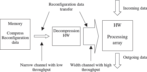
Figure 14.4 Compression used to get around the bandwidth limitation of reconfiguration data transfer
This would then suggest that FPGAs provide a useful platform for developing new types of computer architectures which are memory-orientated, rather than computation-orientated. The text has clearly shown how different circuit architectures were developed for different DSP algorithms. The architectrual derivations were usually driven by creating the necessary computation resources to meet the detailed specifications of the system. There is a strong case for suggesting more detailed research into the development of memory-orientated architectures where some basic principles are developed for creating the memory requirements of some DSP algorithms. This was seen to some extent in the Imagine processor (Kapasi et al. 2002) where the memory was developed for the class of algroithms needed, and in trivial FPGA examples in Chapters 6, 8 and 9, where different memory, i.e. LUTs in the forms of SRLs, was selected in preference to flip-flops to provide more efficient implementation delay chains, either because of lack of flip-flop resource or more relevant selection of resource. However, this has tended to be a good design decision rather than a conscious need to develop memory-orientated architectures. Work by Fischaber et al. (2007) has suggested how design of memory can be directed from the dataflow level.
14.4 Support for Floating-point Arithmetic
A conscious decision to first introduce scalable adder structures in early FPGAs and then dedicated multiplicative complexity in latter versions, such as the such as the Stratix® III family from Altera and the Virtex™-5 FPGA family from Xilinx, has really influenced the use of FPGAs for DSP systems. Along with the availability of distributed memory, this has driven an additional interest in using FPGAs for supercomputing due to the extremely high computation rates required. A number of hardware platforms are now available from a wide range of vendors including solutions from Cray, SGI and Nallatech, and would appear to offer high performance for supercomputing. However, work by Craven and Athanas (2007) would suggest that the performance achievable, even when using many of the techniques highlighted in this book, is limited and that use of FPGA in supercomputing applications, will have limited application.
A key reason for this is the lack of suitable floating-point support in FPGA, even though the work in Craven and Athanas (2007) avoided the use of floating-point arithmetic and used fixed-point hardware. The figures outlined in Chapter 3 and repeated here in Table 14.1, highlight the problems of using floating-point arithmetic in FPGAs. A fixed-point implementation would only need one DSP48 if the wordlength was less than 18 bits, and would not require a lot of the flip-flops outlined in the table. This extra hardware is required to implement the hardware necessary to perform the data selection, rounding and normalization, illustrated earlier in Figure 3.10. If FPGAs are to be used extensively in supercomputing, support for these functions will need to be included in future versions of FPGAs as well as much better high-level programming support for pipelining.
Table 14.1 Area and speed figures for various floating-point operators implemented using Xilinx Virtex-4 FPGA technology
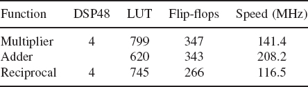
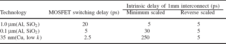
Table 14.2 Impact of technology scaling on interconnect delay (Davis et al. 2001)
14.5 Future Challenges for FPGAs
The offerings in the most recent commercial FPGAs are highly impressive. The recent devices represent highly complex platforms which push the silicon technology and now apparently are used, in preference to memory, as complex devices to test future silicon technologies. However, there are number of challenges that will particularly affect FPGAs.
Technology scaling offers a number of advantages, but it accentuates one particular relationship which is problematic for FPGAs and that is the ratio of interconnect to transistor delay. Some examples of this are shown in Table 14.2 which is taken from (Davis et al. 2001) and shows the ratio of interconnect to transistor delay for various technologies. In this table, minimum scaling represent what will actually happen to the delay if no measures are taken into consideration whereas reverse scaling refers to the impact of fattening the wires, thereby reversing the scaling process. Reverse scaling will be deliberately employed to counteract the increased resistance impact of the interconnect, as indicated in (Table 14.2). Whilst this addresses the timing problems, it causes a dramatic decrease in wiring densities, thereby reducing levels of integration and making larger bus-driven structures inefficient from an area perspective. Given the high dependence of FPGAs on programmable routing, either approach has implications; one, minimum scaling, will act to slow the system considerably whereas the other, reverse scaling, will have a major area impact. It seems likely that the impact of this effect will be to increase the use of larger heterogeneous blocks on FPGAs.
Progressive scaling has driven the semiconductor industry, allowing vendors to deliver faster, cheaper circuits with ever-increasing functionality. A more serious issue than increasing impact due to interconnect delay, is the impact of process variation. With technology at 40 nm and the shift towards sub-10 nm by 2018 (Semiconductor Industry Association 2005), variability in device characteristics now represents a major challenge in delivering next-generation SoC systems, including FPGAs. With other problems it has been possible to adopt the worst case and then use other approaches to overcome the limitations, but with process variation, questions arise about the reasons for investing in next-generation scaling.
References
Bondalapati K and Prasanna V (2002) Reconfigurable computing systems. Proc. IEEE 90(7), 1201–1217.
Brebner G (1999) Tooling up for reconfigurable system design Proc. IEE Coll. on Reconfigurable Systems, pp. 2/1–2/4.
Compton K and Hauck S (2002) Reconfigurable computing: a survey of systems and software. ACM Computing Surveys 34(2), 171–210.
Craven S and Athanas P (2007) Examining the viability of fpga supercomputing. EURASIP Journal on Embedded Systems 1, 13–13.
Davis J, Venkatesan R, Kaloyeros A, Beylansky M, Souri S, Banerjee K, Saraswat K, Rahman A, Reif R and Meindl J (2001) Interconnect limits on gigascale integration (gsi) in the 21st century. Proc. IEEE 89, 305–324.
DeHon A (1996) Dynamically programmable gate arrays: A step toward increased computational density Proc. 4th Canadian Workshop on Field-Programmable Devices, pp. 47–54.
Ebeling C, Cronquist DC and Franklin P (1996) Rapid: Reconfigurable pipeline datapath Proc. 6th Int. Workshop on Field-Programmable Logic and Compilers, pp. 126–135.
Elixent (2005) Reconfigurable algorithm processing (rap) technology. Web publication downloadable from http://www.elixent.com/.
Fischaber S, Woods R and McAllister J (2007) Soc memory hierarchy derivation from dataflow graphs IEEE Workshop on Signal Processing Systems, pp. 469–474.
Flynn MJ, Hung P and Rudd K (1989) Deep-submicron microprocessor design issues. IEEE Micro 19, 11–22.
Hauck S, Li Z and Schwabe EJ (1999) Configuration compression for the xilinx xc6200 fpga. IEEE Trans. Computer-Aided Design of Integrated Circuits and Systems 18(8), 1107–1113.
Heron J, Woods R, Sezer S and Turner RH (2001) Development of a run-time reconfiguration system with low reconfiguration overhead. Journal of VLSI Signal Processing, Special issue on Re-configurable Computing 28(1/2), 97–113.
Kapasi U, Dally W, Rixner S, J.D. O and Khailany B (2002) Virtex5.pdf Proc. 2002 IEEE Int. Conf. on Computer Design: VLSI in Computers and Processors, pp. 282–288.
Kung HT and Leiserson CE (1979) Systolic arrays (for vlsi) Sparse Matrix Proc. 1978, pp. 256–282.
Kung SY (1988) VLSI Array Processors. Prentice Hall, Englewood Cliffs, NJ.
Laufer R, Taylor R and Schmit H (1999) PCI-Piperench and the SWORDAPI – a system for stream-based reconfigurable computing. Proc. IEEE Symp. on Field-programmable Custom Computing Machines, Napa, USA, pp. 200–208.
Li Z and Hauck S (2001) Configuration compression for virtex fpgas Proc. IEEE Conf. on FPGA-based Custom Computing Machines, pp. 147–159.
Luk W, Shirazi N, Guo SR and Cheung PYK (1997) Pipeline morphing and virtual pipelines. 7th Int. Workshop on Field-programmable Logic and Applications, pp. 111–120.
Lysaght P and Stockwood J (1996) A simulation tool for dynamically reconfigurable field programmable gate arrays. IEEE Trans. on VLSI Systems 42(2), 381–390.
MacBeth J and Lysaght P (2001) Dynamically reconfigurable cores Proc. IEEE Conf. on FPGA-based Custom Computing Machines, pp. 462–472.
Maxfield C (2004) The Design Warrior's Guide to FPGAs. Newnes, Burlington.
Scalera SM and Vazquez JR (1998) The design and implementation of a context switching fpga Proc. IEEE Conf. on FPGA-based Custom Computing Machines, pp. 78–85.
Semiconductor Industry Association (2005) International technology roadmap for semiconductors: Design. Web publication downloadable from http://www.itrs.net/Links/2005ITRS/Design2005.pdf.
Todman T, Constantinides G, Wilton S, Cheung P, Luk W and Mencer O (2005) Reconfigurable computing: architectures and design methods. 152(2), 193–205.
Trimberger S, Carberry D, A. J and Wong J (1997) A time-multiplexed fpga Proc. IEEE Conf. on FPGA-based Custom Computing Machines, pp. 22–28.
Walke R, Dudley J and Sadler D (2000) An fpga based digital radar receiver for soft radar Proc. 34th Asilomar Conf. on Signals, Systems, and Computers, pp. 73–78.