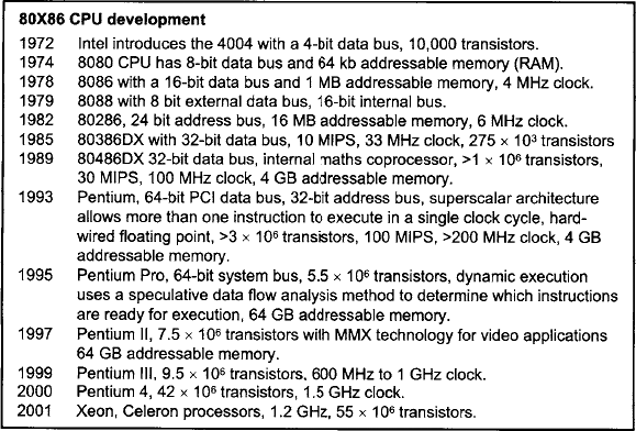
Computer architecture
2.2.1 Computer architecture
The combination of functional components in a computer is referred to as the architecture of the microcomputer. The main functional components in a microcomputer are the CPU or central processing unit, memory, and input/output (I/O) devices:
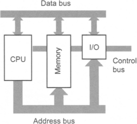
Binary information is transferred as TTL logic across wires called the bus – the address bus, the data bus and the control bus. When an address is placed on the address bus, the byte of information at or for that memory location is placed on the data bus. Signals on the control bus tell the CPU whether a read or write operation to that memory cell is required.
The address bus is unidirectional in that data is placed on it only by the CPU. The 8086 chip has a 20-bit address bus but the internal registers of the CPU are only 16 bits. A special segmented memory addressing scheme is used to obtain access to the full 1 MB memory.
Each memory cell is capable of holding 8 bits, or 1 byte, of data. Memory cells are labelled with a unique address.
The data bus in the 8086 CPU is 16 bits wide and is bi-directional. It can transfer data in both byte and word length to and from the CPU and memory.
The control bus carries various synchronisation and control signals, the only one of interest to us being the read/write signal. This is designated R/W (read/not write). During a read cycle, the processor receives data from either memory or a memory-mapped peripheral device. During a write cycle, the processor sends data to either a memory cell or a memory-mapped device.
2.2.2 Memory
Each memory cell is capable of holding 8 bits, or 1 byte, of data. Memory cells are labelled with a unique address. When the microprocessor wishes to read or write data to a particular memory cell, it places the address of the required cell on the address bus, and the data to or for that memory location appears on the data bus. Internal circuitry ensures that only the memory cell whose address appears on the address bus receives or sends the data from or to the data bus.
The amount of memory that can be addressed by the CPU depends on the width of the address bus. The Intel 8086 CPU has a 20 bit address bus and is able to address a total of 220 = 1 048 576 bytes (1MB of RAM). Each memory cell is numbered $00000 to $FFFFF. However, the internal working registers in the 8088 are only 16 bits wide and a special segmented memory addressing scheme is used to fit the 20-bit address data into the 16-bit registers. In contrast, the 80286 has a 24-bit address bus allowing 16 MB adressable RAM. Later processors employ a 32-bit address bus (486) giving 4 GB addressable memory while Pentium Pro and later processors have 64 GB addressable memory.
Memory is divided into a number of segments, each of which is 64 kb in size:
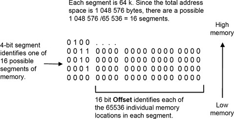
Thus, to specify a particular location in memory, all we need is a 4-bit segment base address and a 16-bit offset.
16 bit Offset identifies each of the 65536 individual memory locations in each segment.
Unfortunately, it is not that simple. Segments need not start on the 64k boundaries shown above. Indeed, segments can start anywhere on a 16-bit boundary since the full 16-bit width of the CPU internal registers can then be utilised.
| Address | data |
| 00F101 | 32 |
| 00F100 | D3 |
| 00E111 | 32 |
Program statements are always stored in the code segment. Data for programs is stored in the data segment etc.
2.2.3 Segmented memory
Here’s how segmented memory really works:
| Segment: | 1010 0111 | 1010 0100 |
| Offset: | 1000 1001 | 1100 1110 |
1. The 16-bit segment is multiplied by 16 to form a 20-bit segment base address by shifting to the left four times.

2. The 16-bit offset is added to the segment base address to obtain the 20-bit absolute address.
3. The segmented address is written with the segment followed by a colon “:” and then the offset. For example:
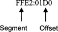
The number obtained after the segment has been added to the offset is called the absolute address.
Note: Since segments can be specified with any 16-bit number, it is possible to have two different segmented addresses which refer to the exact same physical memory location! For example, 0010:0000 is the same as 0000:0100 which is memory location 100H.
Why is it useful to have segments start at any 16-bit address boundary? It permits a more efficient use of memory. For example, a particular program may not need a full 64k code segment. Some of this available memory may be used as the data segment by allowing the segments to overlap. By allowing a 16-bit number to specify the segment (instead of a 4-bit number), the start of each segment can be controlled to within a 16-bit boundary (instead of a 64 k boundary).
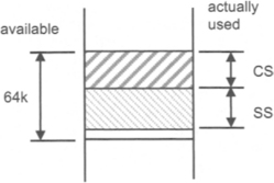
This example shows how the Stack Segment can be accommodated within a 64K block which is only partially used by the Code Segment.
2.2.4 Memory data
Each memory cell can store 8 bits, or 1 byte, of data. The width of the data bus indicates how much data can be transferred during each memory read/write operation. The 8088 CPU has an 8-bit data bus but can actually process 16 bits at a time using its 16-bit internal registers. The 80286 has a full 16-bit data bus. The 80486 has a 32-bit data bus and Pentium processors have a 64-bit data bus.
The contents of memory are interpreted by the CPU as either:
| Data | Logical (1s and 0s indicating T and F) or |
| Numeric – signed or unsigned integers as binary numbers. | |
| Instructions | An assembly or machine language opcode. |
| Address | A “pointer” to which the CPU goes to get the data required. |
Groups of bits larger than a byte are called words. In a 16-bit machine, the term word is used to describe 16-bit (2-byte) data and the term long word or double words for 32-bit (or 4-byte) data. In the 8086 architecture, words are stored in memory with the higher byte in the higher numbered address.
The width of the address bus on the MC 68000 chip is effectively 24 bits (3 bytes). (On the 68000 chip, the address bus is only 23 bits wide numbered A1 to A23 with an internal A0 bit which controls the way the 16-bit data bus is used. The effective bus width is thus 24 bits.) The number of addressable memory locations is:
which are numbered from 0 to 16 777 125 or in hex $000000 to $FFFFFF. Each address refers to a data space of one byte (or 8 bits) giving 16 MB of RAM.
| Address | data |
| 06001 | 3E |
| 06000 | 01 |
In the example here, referencing a word at 06000H, one would obtain: 3E01H. When words and double words start at an address that is a multiple of 4, they are aligned.
Double words take up four memory locations and are stored with the higher word at the higher address pair. Within each word, the higher byte is stored at the higher numbered address. It is usual to write memory addresses from the bottom upwards.
2.2.5 Buffers
Binary signals are transmitted between the CPU and memory cells across the address and data buses. Proper communication of data requires that one and only one memory cell, the one whose address is present on the address bus, has direct connection to the data bus at any one time. Decoding circuitry determines the location of the desired memory cell to be activated. Activation of a single memory cell entails connecting the cell to the data bus and ensuring that all other cells are effectively disconnected. This connection procedure is carried out by tri-state buffers.
The table below shows that the connection between the data bus and a memory location must be set at a high impedance when the chip-select signal CS is low and pass through the data when chip-select is high.
| Data | CS | Connection |
| 0 | 0 | High impedance |
| 1 | 0 | High impedance |
| 0 | 1 | 0 |
| 1 | 1 | 1 |
Buffers isolate memory cells from the data bus and also allow data to pass through during read/write operations. Since the data bus must pass data in both directions, its connections to the bus and the memory cell must be capable of being at TTL high and TTL low (to represent logic levels 0 and 1). When a memory location is not selected (by the decoders), the buffer must effectively disconnect the memory cell from the data bus by inserting a high impedance. The term tri-state means that the connection made by the buffer can be either TTL high, low or high impedance.
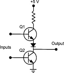
A simple example of tri-state logic can be made using two transistors as shown:
| Q1 | Q2 | Output |
| Off | Off | High impedance |
| Off | On | 0 V |
| On | Off | +5 V |
2.2.6 Latches
A latch is a device which holds the data that appears on its input terminals. A memory cell in the microcomputer system is a latch. Typically, signals destined for storage in memory cells appear on the data bus momentarily and then disappear. The timing of the signals is regulated by the internal clock which runs at speeds typically in the MHz range. The decoding circuitry determines which buffer is to be activated. The activated buffer in turn connects the latch input terminals to the data bus. The signals on the data bus are transferred through buffers to the latch circuit which stores the signals on its output terminals.
A latch circuit can be implemented using a series of RS flip-flops. In this figure, the 4 bit data at D3 to D0 is transferred to Q on the clock pulse. When a bit D is logic 1, S = 1 and R = 0 and the output Q becomes 1. When D is logic 0, S = 0 and R = 1 and the output D = 0.
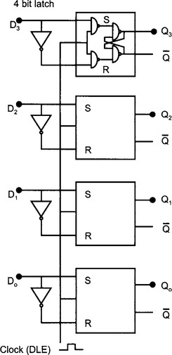
An octal latch has 8 inputs and 8 outputs. The data latch enable (DLE) pin, when set high, copies the voltage levels on the input pins to the corresponding output. The latch circuitry retains the signals on the output pins even if the input signals disappear and DLE goes low. It is important that DLE is set when data appears on the input. DLE is typically timed to go high when data appears on the data bus. The clock signals are used to synchronise this timing.
2.2.7 Flip-flop
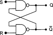
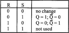
Flip-flops can be used to represent binary numbers. An RS flip-flop is a digital circuit which is stable in one of two states – set or reset. Such a circuit can be made using NAND gates. A truth table summarises the action of flip-flop. The voltage of one of the outputs can be used to represent or store a binary digit since it can be either voltage high (logic 1) or low (logic 0) and will remain at that setting until signals on the input, which only last for a short time, set or reset the outputs.
A microcomputer uses a clocked flip-flop to synchronise the action of the circuit.
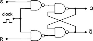
Data at terminal S gets transferred to Q on the clock pulse and remains at Q even if the signal at S disappears and the clock goes low.
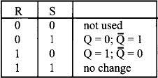
Note: This action table is different to the ordinary NAND flip-flop. Here, R = S = 1 is the “not used” state.
The data stays at Q because when the clock pulse goes low, the flip-flop circuits within the chip are at S = R = 1 (due to the NAND gates on the clock stage). Only when the clock goes high do the flip-flops react to the logic signals at D on the latch.
2.2.8 Input/Output (I/O)
There are three methods of handling input/output devices. The first is by the use of ports. In an 8088-based microcomputer, ports are identified using a 16-bit port number. Thus, there are a total of 65 536 available ports numbered 0 to 65 535. The CPU uses a signal on the control bus to specify that the information on the address bus and data bus refers to a port and not a regular memory location. The port with the specified number then receives or transmits the data from its own inbuilt memory which is not part of the main computer’s memory. However, some devices use main memory for their own use and thus data for these devices may be specified using regular memory addresses. This is the second method used for I/O. Such devices (e.g. video adaptors) are called memory-mapped I/O devices.
This list shows the range of input and output devices for a typical desktop microcomputer. These devices may often by memory-mapped and data is written from/to them via interface adaptors. Some ports are not memory mapped and a signal on the control bus identifies to the CPU that the address is that of a port and not a memory location.
The third method of I/O involves bypassing the CPU and writing or reading directly from memory. This is called direct memory access or DMA. A special DMA controller IC is used to regulate traffic on the bus for this activity. A computer’s disk drive usually transfers data to or from memory using DMA.
2.2.9 Microprocessor unit (MPU/CPU)
The central processing unit organises and orchestrates all activities inside the microcomputer. Each operation within the CPU is actually a very simple task involving the interaction of binary numbers and Boolean algebra. A large number of these simple tasks combine to form a particular function which may appear to be alarmingly complex.
The “MPU” is essentially the same thing as the more familiar and general term “CPU” (CPU applies to any computer, and not just a microcomputer).
The CPU is responsible for initiating transferring data to and from memory and input/output devices, performing arithmetic and logical operations, and controlling the sequencing of all activities. Inside the CPU are various subcomponents such as the arithmetic logic unit (ALU), the instruction decoder, internal registers and various control circuits which synchronise the timing of various signals on the buses.
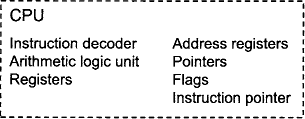
2.2.10 Registers
The 8088/6 CPU has 14 internal registers. All the registers are 16 bits. Registers are used to hold data temporarily while the CPU performs arithmetic and logical operations.
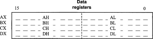
The data registers may be divided into two 8-bit registers depending on whether the CPU is working with 8-bit, or 16-bit data. Within the 16-bit X registers, the 8-bit registers are AL, BL, CL and DL, and AH, BH, CH, and DH. Each half of the X registers may be separately addressed using L and H labels.
• AX is the accumulator and is used as a temporary storage space for data involved in arithmetic and string (character) operations.
• BX is the base register and is often used to hold the offset part of a segmented address during memory transfer operations.
• CX is the count register and is used as a counter for loop operations.
• DX is the data register and is a general purpose 16-bit storage location used in arithmetic and string operations.
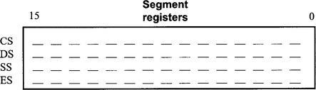
• CS is the code segment and contains the base address of the segment of memory that holds the machine language program that is being executed.
• DS is the data segment and contains the base address of the segment of memory where current data (such as program variables) are stored.
• SS is the stack segment and contains the base address of the stack segment which is used to hold return addresses and register contents during the execution of subroutines within the main program.
• ES is the extra segment and contains the base address of the extra segment which is used to supplement the functions of the data segment.
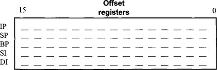
• IP is the instruction pointer (or program counter) which provides the offset address into the code segment (CS) for the address of the next instruction to be executed in a machine language program.
• SP is the stack pointer and together with the base pointer (BP) provide the offset into the stack segment (SS). This is the current location of the top of the stack.
• BP, the base pointer, is used in conjunction with the stack pointer to provide an offset into the stack segment.
• SI and DI are index registers and are used (usually in conjunction with a data register) to provide an offset into the data segment for the processing of long string characters.
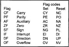
Flags are individual bits which are used to report the results of various comparisons and processes done by the CPU. Program statements may then branch depending on the status of these flags. Although the flags themselves are individual bits, they are arranged together in the form of a 16-bit register so that their contents may be easily saved and restored whenever necessary (e.g. while a subroutine is being executed).
![]()
| Carry flag | arithmetic carry out |
| Parity flag | even number of 1s |
| Auxiliary carry flag | used for BCD arithmetic operations |
| Zero flag | zero result or equal comparison |
| Sign flag | negative result or not equal comparison |
| Trap flag | generates single-step operation |
| Interrupt enable fag | interrupts enabled |
| Direction flag | decrement/increment index registers |
| Overflow flag | arithmetic overflow |
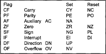
When the status of flags is reported in diagnostic programs, a special notation is used. After executing an instruction, flags are either set (logic 1) or reset (logic 0). Instructions with the CPU’s instruction set use these flags to jump to another section of the current program.
Other instructions exist which allow a program to set or reset some of the flags. The flag register as a whole is usually pushed onto the stack when a subroutine executes and is then popped off the stack when the main program resumes.
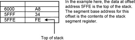
The stack is a block of memory used for temporary storage. Saving data to the stack is called pushing and retrieving the data is called popping. Data pushed onto the stack can be popped off the stack on a last-in, first-out (LIFO) basis. The offset which represents the top of the stack is held in a register – called a stack pointer. The base address is the contents of the stack segment register. Thus, the segmented address of the top of the stack is given by SS:SP. The stack fills from high memory to low. The bottom of the stack is thus: SS:FFFF.
When a subroutine is called within a program, the contents of CS and IP are pushed onto the stack. After the subroutine has finished, CS:IP are popped off the stack and thus execution of the main program resumes at the statement following the call to the subroutine. The subroutine itself can also save the contents of other registers by pushing them onto the stack and then popping them back before handing control back to the main program.
When data is pushed or popped from the stack, the stack pointer (SP) decrements or increments either by 2 or 4 depending on whether a word or a double word is being pushed or popped.
2.2.11 ROM
Conventional memory is called “random access memory” or RAM and is able to be read from or written to. ROM is read only memory and can only be read from. Data in ROM is burned in during manufacture of the memory chip. In an 8086 based microcomputer, there are a number of programs placed in ROM which allow the computer to do certain basic operations. For example, ROM typically contains:
• BIOS (basic input/output services).
• BIOS extensions for additional equipment connected to the computer.
1 Start-up routines
When power is applied to the microcomputer, the first program to run is a power-on-self-test which does a memory check, initialises all support chips and the vector interrupt table, and finally loads the operating system.
2 BIOS
BIOS standards for Basic Input/Output Services and these services are a set of programs which allow application programs to interface with input/output devices connected to the computer in a consistent manner. BIOS programs are usually stored in ROM firmware. The operating system calls upon ROM BIOS routines using interrupts. The ROM BIOS relieves the application program of interfacing directly with memory locations to manage keyboard entry, video output, serial and parallel communications etc.
2.2.12 Interrupts
Servicing of I/O devices is usually done using interrupts. When an interrupt signal is received, the CPU suspends its activities and runs an interrupt service routine or interrupt handler. After the interrupt service routine has finished executing, normal execution is resumed.
There are three types of interrupts:
1 Microprocessor interrupts
These interrupts are initiated by various error conditions (such as a division by zero or arithmetic overflow). These interrupts are also known as processor exceptions.
2 Hardware interrupts
These interrupts are physically wired into the microcomputer. A special NMI interrupt has the highest priority and cannot be masked out by other interrupts. It is processed during critical hardware events such as a power loss.
3 Software interrupts
These interrupts are initiated by software to perform various operations such as writing to a disk file, reading from the serial port etc. These built-in interrupt handling routines are a part of the computer’s BIOS – Basic Input/Output Services.
Interrupts are handled on a priority basis. The interrupt number determines its priority. High level interrupts cannot themselves be executed if a lower level or high priority interrupt is being processed.
The management of hardware interrupts is handled by a programmable interrupt controller chip: the 8259. This chip can be programmed to implement a variety of priority schemes and to accept level or edge-triggered interrupt signals. It determines which interrupt requires servicing and signals the CPU via the INTR line that an interrupt is pending. When an acknowledgement is received from the CPU, the 8259 places the interrupt number on the data bus and the CPU determines the address of the appropriate interrupt handler and the required interrupt service routine is then executed.
An interrupt vector table contains the address pointer for the interrupt service routines associated with each of the 256 available interrupts. The interrupt vector table is usually located in low memory. Interrupt vectors 0 to 31 are usually reserved for microprocessor interrupts. The remainder can be used for hardware or software interrupts.
The interrupt type number determines its place within the interrupt vector table and its priority (with the exception of the NMI interrupt (2), but has the highest priority due to its direct connection with the CPU).
Microprocessor interrupts are divided into fault, trap or abort conditions. For fault conditions, the instruction that caused the fault is retried after the interrupt service routine has been executed. For trap conditions, the next instruction in the program being run by the CPU is executed after execution of the interrupt service routine. Abort conditions stop the main program execution entirely necessitating a restart of the program.
The IF flag is used to control whether or not hardware interrupts can be processed. When a hardware interrupt is recognised, the CPU clears the IF flag automatically, but this can be reset by the interrupt service routine if additional higher priority hardware interrupts are to be serviced during processing of the interrupt service routine.
| Vector | Interrupt |
| 32–255 | Available for software and hardware interrupts |
| 17–31 | Reserved |
| 16 | Coprocessor error |
| 14–15 | Reserved |
| 13 | General protection fault |
| 12 | Stack fault |
| 10–11 | Reserved |
| 9 | Hardware keyboard |
| 8 | Hardware timer |
| 7 | Coprocessor not available |
| 6 | Invalid opcode |
| 5 | Print screen |
| 4 | Overflow |
| 3 | Breakpoint |
| 2 | NMI |
| 1 | Debug/single step |
| 0 | Divide error |
2.2.13 Memory map
Memory is addressed by reference to segments and offsets. However, as we have seen, the actual value of the segment may be on any 16-bit boundary. Memory itself is divided into blocks. There are 16 blocks each of size 64 k (65 536 bytes). Block 0 is the first block and starts at address 00000 and extends to 0FFFF. Block 1 starts at 10000 and goes to 1FFFF etc.

2.2.14 Real and protected mode CPU operation
80286 processors and above can operate in either real or protected mode. When operating in real mode, the CPU can execute the base instruction set of the 8086/8088 processors. In protected mode, the CPU makes use of advanced features for memory management and multi-tasking under the Windows operating system. In protected mode, 80386+ processors can act in virtual 8086 mode allowing 8086 instructions to run in a “DOS” window.
Multitasking under Windows requires programs running on the computer to be isolated from each other and a protected mode of operation is thus required. In protected mode, a program cannot write directly to memory. Instead, any data to be written or read is done to virtual memory space and transferred to physical memory using a process called virtual-to-physical translation by the CPU.
When operating in protected mode, the CPU register structure is different to that used in real mode. The most important additions are descriptor tables which hold information about memory and interrupts for each task being run. Details of each task or application being run on the microprocessor are held in the task register.
Each task is assigned global and local memory resources. All tasks can access the global address space, but a task cannot access another task’s local address space.
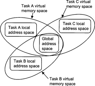
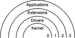
Each task is also assigned a privilege level. The kernel is responsible for low level tasks such as memory management, I/O and task sequencing. The kernel has the highest privilege level: 0.
Tasks with a lower privilege level can use routines that have a higher privilege level but cannot modify them. User applications programs are assigned the lowest privilege level: 3.
The combination of local address space and hierarchy of privilege levels allows the instructions and data for all the running tasks to be isolated from each other. Data in one task is thus protected from errors arising in another task.
Unlike real mode operation, I/O operations from a user application do not have the required privilege level and so must perform these functions in conjunction with an I/O device driver which does. This ensures that I/O is done without violating not only the address space of another running application, but also that the I/O does not adversely affect the low level task sequencing and memory management responsibilities of the CPU.
The significance of protected mode operation for interfacing is that when multiple tasks or applications are being run by the CPU, it appears to the user that they are operating simultaneously whereas task activity is actually time-shared within the CPU. For time-critical interfacing applications, the user must be aware of the limitations imposed by this time sharing and hierarchy of privileges. Virtual device drivers (VxD) typically have a kernel level of privilege that permits direct I/O and this, together with direct memory access, are required for time-critical interface applications.
When a DOS program is run in a DOS or command window within a Windows environment, the CPU is placed into virtual 8086 mode by setting the VM flag in the extended flag register. The DOS program is still run as a protected mode task, and when the CPU switches to this task, the VM flag is set as part of the task switching process. The DOS mode program is assigned a privilege level of 3. The memory addressing scheme of the task simulates that of a real mode CPU operation and can be configured as part of the task properties.
2.2.15 Review questions
1. Give brief answers to the following questions:
(a) How many memory locations (or memory cells) can be addressed by a 8086 microprocessor and why?
(b) What is the largest (unsigned) hexadecimal number that can be stored in one memory location and why?
(c) How many memory locations can be read in one read/write cycle and why?
2. List the four types of special internal registers that exist in the 8086 microprocessor.
3. Explain the difference between a port and an address.
4. Draw a diagram which outlines the main components of a microcomputer system (e.g. the CPU, memory etc). Describe the function of each main component and how each communicates with the others. Indicate also what governs the amount of memory addressable by a program.
6. Which bit in the flags register indicates whether or not a subtraction operation produced a negative result.
2.2.16 Activities
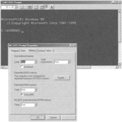
1. Start your computer into DOS mode, or open a DOS command window from your Windows environment.
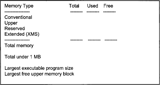
2. Enter the mem command from the DOS prompt and determine how much RAM memory your computer is fitted with and how it has been allocated. Fill in the table below with the values shown on your screen.
3. Start the debug program by typing the command debug at the DOS prompt. The debug prompt is a “-” character and indicates debug is ready for a command.
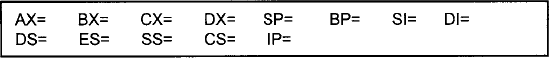
4. Enter the r command and display the contents of the registers. Fill in the table with the values indicated on your screen (include the last line of the debug output in this table).
5. What is the status of all the flags? Are they set or reset? Is there any one flag that is set differently to the others? Why would this be?
6. The last line in the register listing displays machine code and assembly language of the instruction pointed to by the CS:IP registers. Compare the segmented address at the beginning of this line with the indicated contents of the CS and IP registers. CS: ______ IP: ________
7. To list the contents of a single register, we enter r XX where XX is the register name. Debug responds with the current contents of the register and then allows us to change those contents. Display the contents of the AX register and change it to 00FE.
8. To display the flags, we enter r f at the debug prompt. We can then set any of the flags by entering in the appropriate flag code. Display the flags and then change the parity flag to even.
| AX | accumulator |
| BX | base |
| CX | count |
| DX | data |
| CS | code segment |
| DS | data segment |
| SS | stack segment |
| ES | extra segment |
| IP | instruction pointer |
| SP | stack pointer |
| BP | base pointer |
| SI | source index |
| DI | destination index |
9. The “memory dump” command is d. The syntax is:
If the segment base address is not specified, then the address is taken to be the offset to the current contents of the DS register. Examine the contents of the BIOS area of memory which is located at F000:0000. Note that the d command displays 128 bytes starting at the address you specify. The d command lists the memory contents in hex and attempts to interpret any ASCII characters and if any are found to be valid ASCII, the characters are displayed on the right-hand side of the screen. Continue to display the contents of the BIOS area of memory until you find the copyright message from the manufacturer of your computer. Record the memory location at which the copyright message appears. ______: ________
You can continue to press d without any parameters to display more memory contents. Some very interesting messages can be found in the BIOS contents.
10. Debug permits the display, enter, fill, move, compare and search for data in memory. The “enter” command e, allows us to change the contents of memory. The syntax is: e [address] [data].
Enter the value FF into memory location DS:0000 by typing: e DS:0000 FF. Verify that the contents of DS:0000 have changed by entering e ds:0000 and then pressing <enter> key to terminate enter mode.
11. The “fill” command fills a block of memory with all the same values. The syntax is: f [start address] [end address] [data].
Initialise memory locations DS:0000 to 0100 with zeros. Note: the end address parameter is specified with an offset only and is assumed to be the same as that as the starting address. Verify the contents of these memory locations with the d command.
12. The “move” command allows us to copy a block of memory from one place to another in memory. The syntax is:m [start address] [end address] [destination address]. Again, the segment base address is either implied (the DS register contents) or specified within the start address. Move the contents of DS:0000 to DS:0100 to DS:0200.
13. The “search” command allows us to scan a block of memory and search for a specific byte The syntax is:s [start address] [end address] [data].
The address for any matches is displayed. Search memory locations F000:0000 to F000:FFFF for the characters “read failure”.
Character data may be entered in a debug command if it is delimited by quote marks. When debug processes the command, the ASCII value of the characters is substituted.
Display the contents of nearby memory locations with the d command.
14. In addition to loading and running machine language programs (which we will investigate in the next laboratory session), debug also is a handy hexadecimal calculator. The h command allows us to add and subtract hex numbers. Both operations are performed by the same command.
The syntax is: h [hex number 1] [hex number 2] and the sum and difference of the two numbers is displayed (in hex).