Interfacing
2.4.1 Interfacing
The term interfacing is used to describe the connection between a transducer or some other external device and the microcomputer. Interfacing circuits may be required to deal with various levels of incompatibility:
Mechanical or electronic devices requiring connection to the microprocessor unit can be anything from the output screen or monitor, the keyboard, and external instruments. Two main problems are usually encountered when interfacing such devices:
• Most devices do not operate at the same speed as the microprocessor.
• There may be more than one device which requires servicing at any one time.
A port is a connection from the outside world to the microprocessor. The purpose of an input port is to transfer information from the outside world to the microprocessor. An output port provides information to the outside world from the microprocessor. Each port has an address and is thus connected to the address bus and information to or from the port is transmitted over the data bus. From the microprocessor’s point of view, a port is very similar to a location in memory.
Ports may be memory mapped, interfacing direct to the computer’s RAM, or be assigned a separate port address. An interface adaptor connects the data bus to the I/O device using compatible signals when the port is accessed by the CPU for read/write operations.
2.4.2 Input/Output ports
In an 8086-based microcomputer, I/O ports are identified using a 16-bit port number or port address. Thus, there are a total of 65 536 possible ports numbered 0 to 65 535 (FFFF). The CPU uses a signal on the control bus to specify that the information on the address bus and data bus refers to a port and not a regular memory location. The port with the specified number then receives or transmits the data from its own internal memory.
Input ports generally require servicing (i.e. their data to be read) at irregular intervals and further, their signals may only appear momentarily. Techniques such as polling, interrupts and direct memory access are used to service ports as required.
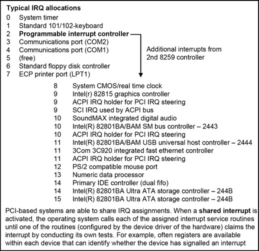
| Port number | I/O device |
| 0000 − 001F | Direct memory access controller |
| 0020 − 003F | Programmable interrupt controller |
| 0040 − 005F | System timer |
| 0060 − 0060 | Standard 101/102-key keyboard |
| 0061 − 0061 | System speaker |
| 0062 − 0063 | System board extension for ACPI BIOS |
| 0064 − 0064 | Standard 101/102-key keyboard |
| 0065 − 006F | System board extension for ACPI BIOS |
| 0070 − 007F | System CMOS/real time clock |
| 0080 − 009F | Direct memory access controller |
| 00A0 − 00BF | Programmable interrupt controller |
| 00C0 − 00DF | Direct memory access controller |
| 00E0 − 00EF | System board extension for ACPI BIOS |
| 00F0 − 00FF | Numeric data processor |
| 0170 − 0177 | Intel(R) 82801BA Ultra ATA storage controller − 244B |
| 0170 − 0177 | Secondary IDE controller (dual fifo) |
| 01F0 − 01F7 | Intel(R) 82801BA Ultra ATA storage controller − 244B |
| 01F0 − 01F7 | Primary IDE controller (dual fifo) |
| 02F8 − 02FF | Communications port (COM2) |
| 0376 − 0376 | Intel(R) 82801BA Ultra ATA storage controller − 244B |
| 0376 − 0376 | Secondary IDE controller (dual fifo) |
| 0378 − 037F | ECP printer port (LPT1) |
| 03B0 − 03BB | Intel(r) 82815 graphics controller |
| 03C0 − 03DF | Intel(r) 82815 graphics controller |
| 03F0 − 03F5 | Standard floppy disk controller |
| 03F6 − 03F6 | Intel(R) 82801BA Ultra ATA storage controller − 244B |
| 03F6 − 03F6 | Primary IDE controller (dual fifo) |
| 03F7 − 03F7 | Standard floppy disk controller |
| 03F8 − 03FF | Communications port (COM1) |
| 04D0 − 04D1 | Programmable interrupt controller |
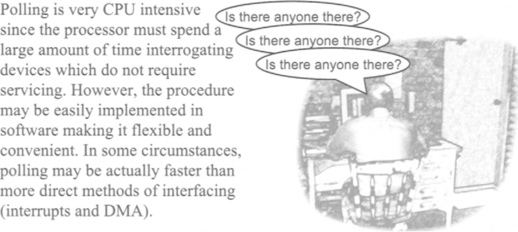
2.4.3 Polling
The easiest method of determining when a device requires servicing is to ask it. This is called polling. In this method, the CPU continually and sequentially interrogates each device. If a device requires servicing, then the request (or bus access) is granted. If the device does not require servicing, then CPU interrogates the next device.
2.4.4 Interrupts
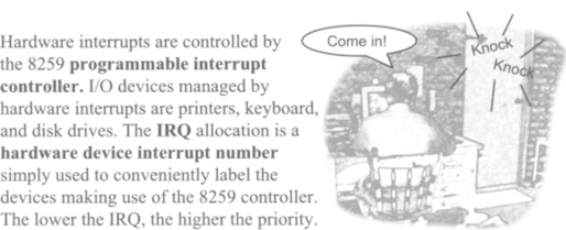
For interfacing applications, the time taken to register and process an interrupt (interrupt latency) can lead to the need for the I/O device to be heavily buffered. In addition, time critical interfacing applications may not work as desired.
2.4.5 Direct memory access (DMA)
In normal data transfer, data is transferred from one memory location to another through registers in the CPU. The CPU has to hold the data temporarily while it switches the control bus signal from a read to a write since the data bus cannot be in a read state and a write state at the same time. This temporary storage of data and resulting transfers into and out of the CPU is time consuming and wasteful for interfacing applications that
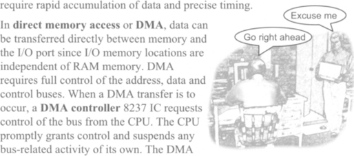
controller then transfers data from port to memory, or memory to port directly, without any stack or register overhead operations that would normally be required by the CPU to accomplish the same task. The DMA acts as a third party to the data transfer. The latency time associated with DMA transfer is only a few CPU cycles.
The 8237 DMA controller has a number of independent channels, each of which is assigned to a particular device. Channel 2 is usually assigned to the floppy disk controller. DMA can take place as a single byte or word, a block of bytes, or on demand up to a set number of bytes. DMA transfers can be initiated by a hardware request (via DREQ input on the 8237) or a software request using a request register.
With a PCI bus, DMA management can be performed not only with the DMA controller, but also by the device requiring DMA access. In such systems, the device that gains control of the bus is called the bus master. For interfacing applications, the combination of bus-mastering DMA and a high speed PCI bus ensures that data transfer occurs as fast as possible from the I/O device to memory. Further, bus-mastering DMA does not require the allocation and usage of DMA channels since the DMA controller is not involved. Bus-mastering DMA is referred to as first party DMA since the I/O device itself is handling all the data transfer.
2.4.6 Serial port
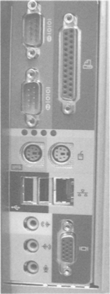
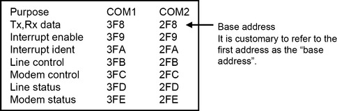
Most microcomputers are fitted with one and often two serial ports. These serial ports are labelled COM1 and COM2. The numbers 1 and 2 are for our “external” convenience only. The actual “internal” port numbers or addresses are 3F8 for COM1 and 2F8 for COM2.
The COM ports can usually be found on the back panel of a microcomputer and may take the form of either 25 or 9 pin connectors. These pins are connected to buffers which convert the pin voltages used for data transmission over external cables (usually using the RS232 standard) to TTL levels used for data transfer within the computer. The internal signals are generated by a special communications IC called a UART.
The serial port is most often used for data communications. Hence, one of the signal lines carries data either being transmitted from, or received by, the computer. The other signals are used to control the flow of data and to establish a communications link between the two serial ports on two different computers. Often, the serial ports are connected by a modem which converts digital data into analog signals for transmission over a telephone line.
The handling and control of transmission is done by setting and reading the binary data which appears in the internal registers of the UART. Each of these registers has an address (i.e. the port address) in the port address space of the computer.

2.4.7 Serial port addresses
The port addresses for IBM compatible microcomputers have been standardised for many years.

Each port address is a register that allows the serial port to be initialised and operated on by software commands. That is, the serial port controller ship, the 8250 UART, is programmable in the sense that its operation can be controlled by software rather than hardwired circuitry.
When a serial port interface card is added to a computer, the base address must be set, either by a jumper on the card, or by software. This allows the card to be configured as COM1 or COM2 (or even COM3 or COM4) as desired.
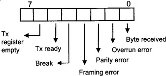
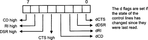
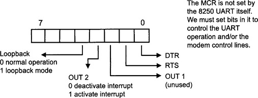
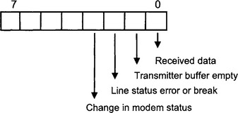
2.4.9 Serial port registers and interrupts
It is most common to operate the serial port (i.e. such as the 8250 UART) through the use of interrupts. However, this need not always be the case. The 8250 has four internal interrupt signals which can be connected through to the CPU’s IRQ interrupt line via an INTR pin on the UART. The OUT2 bit in the Modem Control Register specifies whether or not to connect the UART INTR output to the CPU’s IRQ line. In this way, the internal interrupts generated by the UART can be optionally used by the CPU.
Note: COM1 usually uses IRQ4 and COM2 IRQ3 on the CPU.
A 1 in the corresponding bit position enables the internal interrupt. This will not be registered at the CPU IRQ line unless OUT2 in the MCR is also set to 1.
IER (Interrupt Enable Register)
IIR (Interrupt Identification Register)

2.4.10 Serial port baud rate
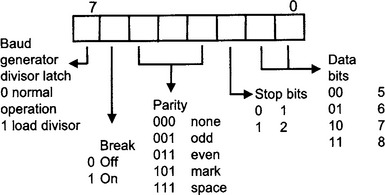
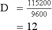
The baud rate is a measure of the number of bits per second that can be transmitted or received by the UART. This rate is regulated by a clock circuit which, for most UARTS, is on the chip itself and can be programmed.

where D is called the baud rate divisor and must be loaded into the UART.
1. Bit 7 of the LCR must be set to 1.
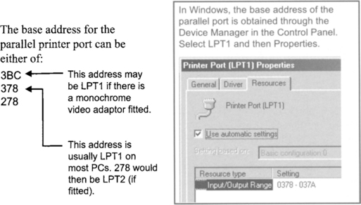
2. The LSB of D is written to the port base address (e.g. 3F8 for COM1).
3. The MSB of D is written to the port base address +1 (e.g. 3F9).
4. Bit 7 of LCR is cleared (and perhaps also set for other parameters such as baud rate, stop bits etc).
5. Check port base address +1 for the desired interrupt settings.
The UART clock must operate at 16 times the desired baud rate. The clock is based around the operation of a crystal oscillator which, in the case of a 8250 UART, is set to a constant 1.8432 MHz. This clock signal is stepped down through a series of counters to obtain the desired clock rate for the chip to give the desired baud rate.
2.4.11 Serial port operation
Although it is possible to write and read from the serial port registers directly, it is more convenient to use either applications’ program languages or BIOS service routines. Most applications’ languages have statements or functions available which facilitate the programming of the serial port. For example, the
statement in BASIC allows the serial port to be configured without a detailed knowledge of the actual port addresses. However, for interfacing applications, direct manipulation of the registers is required. For example, the BIOS service routines on an IBM compatible PC do not provide a way to set RTS for hardware handshaking.
In Visual Basic, it is necessary to make use of the serial port object.
MSComm1 has properties that can be set in code that allow the serial port to which is is assigned to be configured.
![]()
These high level instructions ultimately result in a series of assembly language instructions which call BIOS service routines through the interrupt system.
| The serial port initialisation parameters are: baud rate, parity, stop bits, data bits. They are combined into an 8-bit number which is loaded into AL prior to calling the interrupt. | The service to be called (0 for initialise serial port) is placed into AH. Parameters for the service are placed in AL. The interrupt is called, and the results placed in AL (or AX for service 3), e.g.: |
| mov AH, 0 | |
| int 14H |
2.4.12 Parallel printer port
The parallel port normally found on microcomputers is generally used for printer output although there are some input lines which are used to report printer status (such as paper out etc.). The Centronics printer interface consists of 8 data lines, a data strobe, and acknowledge, three control and four status lines.

The printer port is driven by the parallel port adaptor. In the adaptor, there are three registers which are assigned I/O port addresses. The byte to be printed is held in the data register which is at the port base address. The printer status register contains the information sent to the computer by the printer, and has an address of base+1. The printer control register has address base+2 and contains the bit settings for computer control of printer functions.
2.4.13 Parallel port registers
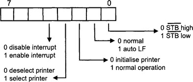
Printer port data register (base) 378
![]()
Printer port status register (base+1) 379

Printer port control register (base +2) 37A
2.4.14 Parallel printer port operation
Although it is possible to write directly to the parallel printer port registers, it is customary to use the BIOS service routines available through the computer’s operating system. Mostly this is done indirectly through high level program statements like PRINT. However, it is possible (and sometimes desirable) to call the BIOS routines directly from an assembly language program.
BIOS routines are called through interrupt 17H. Three services are available and are selected by the value placed in AH. For writing a byte to the printer, the data to be printed is put into AL. The DX register is set to indicate the LPT port to use (0 for LPT1:).
| AH | BIOS service |
| 00 | Write byte |
| 01 | Initialise printer |
| 10 | Report printer status |
After the service has been executed, the contents of the printer status register are reported in AL.

When the printer port is being used through the BIOS service routines or being accessed directly, the following sequence is required to write the data:
• The data to be written is placed in the Printer Port Data Register. That is, the byte is written to the printer port base address.
• The readiness of the printer to accept data is confirmed by testing the bits in the Printer Port Status Register.
• The STB line is then pulsed low by writing a 1 to bit 0 of the Printer Port Control Register. This transfers the data from the Printer Port Data Register to the Data Lines on the port connector.
2.4.15 Review questions
1. Arrange the following statements, which describe the sequence of events when a CPU services an interrupt-driven device, in the correct order.
(a) The return address (i.e. contents of the program counter) is placed on the stack.
(b) The CPU is directed to the interrupt service routine.
(c) The CPU returns to the main program.
(d) The interrupt service routine is executed.
(e) The CPU checks the interrupt mask.
(f) The return address is put back into the program counter PC.
2. Briefly describe the difference between programmed and interrupt-driven I/O.
3. What are the three different types of interrupts in an 8086 CPU-based computer?
4. How many channels are offered by an 8259 DMA controller? How can further channels be accommodated?
5. What is the difference between bus-mastering DMA and DMA via 8259?
6. What should the contents of the Line Control Register be for a UART to be configured for 7 data bits, 1 stop bit, and even parity?
7. What is the main difference between serial and parallel communications? Give examples of advantages and disadvantages of each method.
8. How is data usually communicated out through the parallel port?
9. For interfacing applications, what limits the maximum speed of data acquisition in polling, interrupts, and DMA?