
A to D and D to A conversions
2.5.1 Interfacing
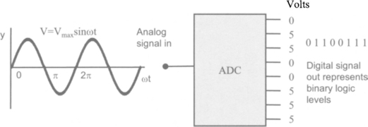
Interfacing to a microcomputer is the process whereby the physical phenomenon to be measured is converted into an analog electrical signal by a transducer. The signal is then digitised by an analog to digital converter (ADC) and then stored in memory.
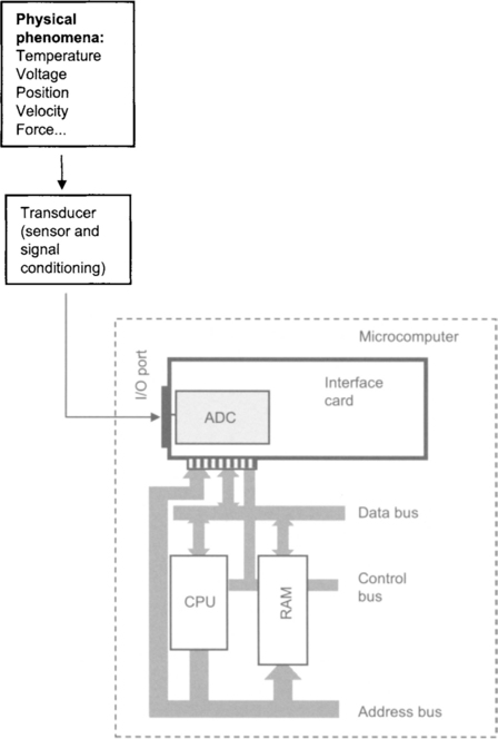
The ADC can be located either near the transducer, or, as is more common, on a special purpose interface card installed inside the microcomputer. The interface card interfaces directly to memory either by DMA or as a memory-mapped device.
When a digital number is to be displayed on some external device, it is converted into an analog electrical signal by an interface adaptor containing a digital to analog converter (DAC). The actuator then converts the analog signal into a physical quantity.
2.5.2 The Nyquist criterion
An analog signal varies continuously with time. A good example is a sine wave of frequency ω.
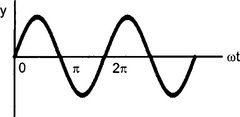
If we were to store this wave as a sequence of numerical data, we would choose data pairs (y, t) at convenient intervals. The smaller the interval, the more accurate the representation of the original signal when we come to reconstruct it from the data.
| 0 | 0 |
| π/4 | 0.797 |
| π/2 | 1 |
| 3π/4 | 0.707 |
| π | 0 |
| 5π/4 | −0.707 |
| 3π/2 | −1 |
| 7π/4 | −0.707 |
| 2π | 0 |
In this example, data was sampled at π/4 or 45o intervals. If we decreased the sampling interval to π/8 (i.e. an increase in the sampling rate), then we would obtain a more accurate representation of the original analog curve.
What minimum sampling rate is required to reconstruct the signal? The Nyquist criterion states that the sampling rate (samples per second) should be greater than twice the highest frequency component (cycles per second) of the signal.

If the signal was sampled at intervals greater than π, then the resultant wave, when reconstructed, may still be a sine wave but at a different (lower) frequency. This is called aliasing. The reconstructed signal is an alias for the original signal.
2.5.3 Resolution and quantisation noise
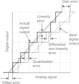
Now, a very interesting problem arises when analog data is to be stored in a digital system like a computer. The problem is that the data can only be represented by the range of numbers allowed for by the analog to digital converter. For example, for an 8-bit ADC, then the magnitude of the full range of the original analog data would have to be distributed between the binary numbers 00000000 to 11111111, or 0 to 255 in decimal. Numbers that don’t fit exactly with an 8-bit integer have to be rounded up or down to the nearest one and then stored.
If the ADC were able to accept input voltages from 0 to 5 volts, then full scale, or 5 volts, on the input would correspond to the number 255 on the output. The resolution of the ADC would be:
Thus, for an input range of 0 to 5 volts, in this example, the resolution of the ADC would be 19.6 mV per bit or 0.39%. A 12-bit ADC would have a resolution of 1.22 mV per bit (0.02%) since it may divide the 5 volts into 4095 steps rather than 255.
In general, the resolution of an N bit ADC is:
where Vref is the range of input for the ADC in volts.
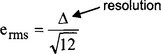
The quantisation error Δe is ± half a bit (LSB) and describes the inherent fundamental error associated with the process of dividing a continuous analog signal into a finite number of bits.
The quantisation error is random, in that rounding up or down of the signal will occur with equal probability. This randomness leads to the digital signal containing quantisation noise, of a fixed amplitude, and a uniform spread of frequencies. The rms value in volts of the quantisation noise signal is given by:
The quantization noise level places a limit on the signal to noise ratio achievable with a particular ADC.
2.5.4 Oversampling
In general, an input signal is comprised of a range of individual or component frequencies. These signals can be separated by Fourier analysis. The range of component frequencies able to be handled by a particular analog to digital converter circuit is called the bandwidth.
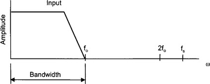
The Nyquist criterion requires us to sample the input at a frequency of at least twice that of the highest frequency component of the input signal: fs ![]() 2fo
2fo
The ratio of the sampling frequency to the Nyquist frequency is called the oversampling ratio: OSR = fs/2fo.
Even if the Nyquist criterion is satisfied, then the existence of the quantisation noise limits the ability of the system to represent the original input signal exactly. This noise, the amplitude of which is independent of the frequency of the signal, becomes a component part of the sampled data. The power associated with this noise Pn is found by integrating erms over the frequency range 0 to fo to give:
where ![]()
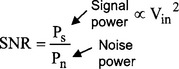
The significance of this is that the signal-to-noise ratio SNR can be improved by increasing the OSR or increasing N.
Now, the noise voltage is expressed here as an rms value, thus, we must also express the input voltage as an rms value. The maximum SNR is obtained when the full range of the ADC is used. Allowing for both positive and negative halves of the input cycle, the maximum value of Vin to the ADC is Vin = Vref/2, and thus, the rms value of this is: ![]() .
.
Increasing the number of bits increases the signal to noise ratio. However, oversampling with an N-bit ADC also reduces the noise power and thus causes the N-bit ADC perform as if it were an N+w bit ADC. If fs is the original sampling frequency, then to obtain w extra bits of resolution, the new (or oversampling) frequency is given by 4wfs.
2.5.5 Analog to digital converters
An analog to digital converter accepts an input voltage and issues a positive integer on its output whose binary value is proportional to the magnitude of the input voltage.
Digital data can be readily stored and processed on a microcomputer. Analog signals cannot.
• Linearity error typically ±1/2LSB
• Differential error typically ±1/2 LSB
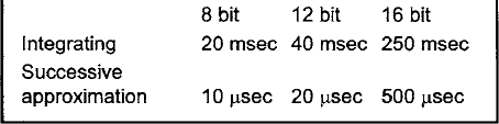
2.5.6 ADC (integrating method)
A to D conversions are usually performed by comparing the unknown input signal voltage to an internal reference voltage. A voltage generator supplies a reference voltage which is adjusted until it equals (to within some predefined tolerance level) the input signal voltage.
The reference voltage is linearly increased in small steps until it equals or exceeds the signal voltage and a digital counter is used to record the number of voltage steps tested during the conversion time. The digital count is thus an indication of the magnitude of the voltage input.
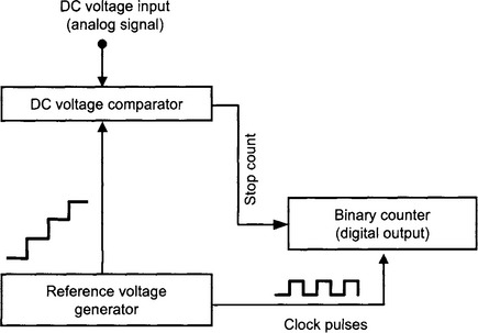
The conversion time depends upon the magnitude of the input voltage. This type of ADC is suitable for recording signals that do not change rapidly with time. The digitised output value represents the average value (or integral) of the input signal over the sampling period.
In more sophisticated devices, a dual slope technique is used. After an initial zeroing period, the analog input signal is integrated (added together) for a fixed number of clock cycles. The integrator input is then connected to an internal reference voltage that has a polarity opposite to the analog input signal.
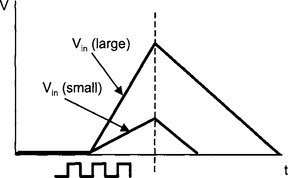
The number of clock cycles for the integrator to “discharge” to zero is proportional to the magnitude of the original analog signal voltage. The accuracy of the ADC is thus dependent on the accuracy of the reference voltage.
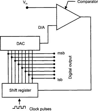
2.5.7 ADC (successive approximation)
In this method, the input voltage is compared to half the full scale voltage and then lower values in succession. The steps are:
3. If Vin > D/A, then Vin is above half of full scale of output, thus, keep a 1 in msb. If not, then clear msb to zero.
4. Set next msb to 1 (i.e. could have 1100 0000 or 0100 0000).
5. If Vin > D/A, then Vin is above 7/8 of fsd, thus, keep 1, else clear bit.
6. Set next msb to 1 (e.g. 0010 0000, 0110 0000, 1010 0000 or 1110 0000)
7. If Vin > D/A then Vin is above 6/8 of fsd, thus, keep 1, else, clear bit position.
and so on until Vin is tested against lsb.
The conversion time is fixed and is equal to: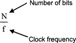
This method allows high speed data acquisition (up to 100 000 conversions/sec). However, the opportunity for errors to be introduced is greater. The fixed conversion time means that the input signal needs to be steady or at least captured during the sampling period.
2.5.8 Aperture error
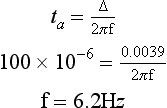
We have seen that the conversion of an analog signal to a digital output takes time: the conversion time, which in the case of a successive approximation ADC, is fixed. Now, if the analog input signal is changing during the conversion time, then the converted output will be in error. This is known as aperture error.
For example, for an 8-bit ADC, the smallest increment δ of input signal registered by a single bit will be: δ = 1/28 = 0.0039 fraction of full scale of signal.
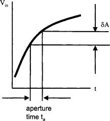
During conversion time, the signal changes. For there to be no error in the digitised output, this change must be less than the smallest increment registered by a single bit: i.e. the product (δ)(A).
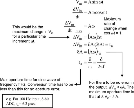
The aperture time is the maximum time interval within which the conversion must occur before the signal changes enough to affect the digitised output.
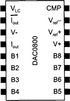
2.5.9 ADC08xx chip
The ADC08xx series of ICs are 8-bit analog to digital converters which use the successive approximation technique.
The conversion time is given by the clock frequency. It takes approximately 64 clock cycles to perform one 8-bit conversion. Thus, to obtain a sampling rate of say 10 000 samples per second, the clock frequency needs to be set to:
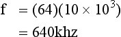
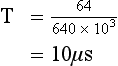
64 clock cycles for one conversion, 640 × 103 clock cycles per second.
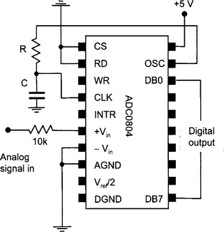
Conversions are initiated by an external start pulse at pin WR. Conversions begin when WR goes from low to high. WR must remain high during conversion.
When conversion is completed, INTR goes low indicating that the digital data on the outputs is complete and the device is ready for the next conversion.
The chip takes the difference between the two analog inputs as its input signal. If −Vin is tied to ground, then the other may be used as a single-ended input. If no external reference voltage is applied at Vref/2, then the chip uses an internal reference which depends on the value of Vcc.
There is an RC oscillator built into the chip whose frequency is approximately 1/RC. For example:
2.5.10 Sample-and-hold
To avoid aperture error, the conversion time and the desired performance characteristics of the ADC circuit must be taken into consideration. For example, given a conversion time of say 100 μsec, what is the maximum frequency of sine wave that can be sampled by the 8-bit ADC0804 without aperture error?
For an 8-bit ADC, δ = 1/28 = 0.0039
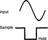
We need a circuit that will take a sample of the input voltage at a particular instant, and hold it until the ADC has processed the conversion - a sample-and-hold circuit. There are a number of pre-packaged ICs available, a common one being the LF198, 298, 398 series.
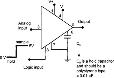
When logic input is high, output follows any changes in the analog input. When logic input goes low, the analog input signal is captured and passed through to the output. Output remains fixed at this value while logic input is held low.
The time taken for the sample-and-hold circuit to sample the signal and hold it must be shorter than the conversion time (otherwise we wouldn’t need to use the circuit!). The above circuit has a conversion time of about 10 μsec.
2.5.11 Sample-and-hold control
Now, to control a sample-and-hold circuit, signals from the ADC can be used.
WR: Standby mode when WR is low. Conversions begin when WR goes from low to high. WR must remain high during conversion.
INTR: Usually high. When conversion is completed, INTR goes low for eight clocks. WR must then be held low for about 500 nsec before going high to initiate a new conversion.
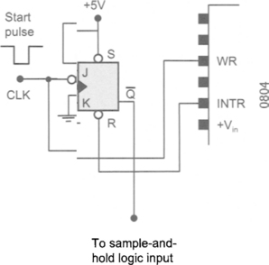
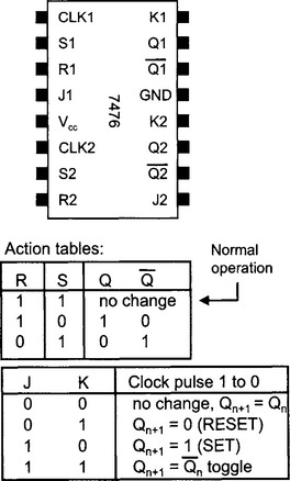
We can use a 7476 latch to control a sample-and-hold circuit. The ![]() output from the latch can be made low while conversion is in progress thus sending the sample-and-hold circuit to “hold”.
output from the latch can be made low while conversion is in progress thus sending the sample-and-hold circuit to “hold”.
• Start pulse initiates conversion since it is connected directly to WR.
• Since ![]() is high, and initially
is high, and initially ![]() is high, the output
is high, the output ![]() will respond to the clock going low and since J is high (with K low),
will respond to the clock going low and since J is high (with K low), ![]() is sent low. Sample will be latched on clock signal going low. Conversion actually begins when clock (WR) goes back high.
is sent low. Sample will be latched on clock signal going low. Conversion actually begins when clock (WR) goes back high.
• At the end of conversion, INTR goes low which sends a low to ![]() sending
sending ![]() high independent of the signal at J and sending sample and hold to “sample”.
high independent of the signal at J and sending sample and hold to “sample”.
2.5.12 Digital to analog conversion
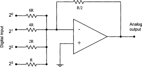
Digital to analog conversions can be performed using resistor networks and the conversion to an analog signal is usually in the order of nanoseconds. Since the digital information is a step approximation of the input signal, the resulting output from a D to A converter reflects this step nature of the signal.

Digital to analog conversions may be made using a ladder network of resistors or a weighted input to a summing amplifier. The voltage on the output depends upon the voltages applied to the inputs. These voltages may be either 0 (for logic 0) or some supply voltage Vcc (for logic 1). The TTL input connected to the lowest value resistor carries more weight than the others, thus, a larger binary or digital input results in a larger analog output voltage.
2.5.13 DAC0800
A popular all-purpose 8-bit D to A converter IC is the DAC080x series. The settling time is in the order of 100 ns.
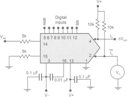
The output for this IC is in the form of two complementary currents Io and ![]() . In the diagram above, these current outputs are connected to a V+ supply through two 10K resistors. A voltage output can be obtained by measuring the voltage between the two output terminals or measuring the voltage of one of the outputs with respect to ground. As the binary value of the digital inputs increases, Io increases and
. In the diagram above, these current outputs are connected to a V+ supply through two 10K resistors. A voltage output can be obtained by measuring the voltage between the two output terminals or measuring the voltage of one of the outputs with respect to ground. As the binary value of the digital inputs increases, Io increases and ![]() decreases. A decrease in
decreases. A decrease in ![]() means an decrease in the voltage drop across the 10k resistor and an increase in Vo measured w.r.t. ground.
means an decrease in the voltage drop across the 10k resistor and an increase in Vo measured w.r.t. ground.
Vref provides a current reference. Setting Vref to V+ makes Vo swing positive and negative. Setting Vo to V+/2 gives a 0 to V+ analog output.
2.5.14 Data acquisition board
In most circumstances, one would accomplish most interfacing tasks with a general-purpose data acquisition board. Such boards fit into an ISA or PCI slot in a microcomputer and would typically contain:
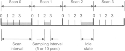
Multiplexing is used on the input to a single ADC chip to allow multiple and continuous scans of the analog inputs. Interface boards generally allow the 16 analog inputs to be open-ended, or paired to form eight differential inputs. The analog inputs may be fitted with simultaneous sample-and-hold circuits to reduce the error associated with sequential sampling of the inputs by the multiplexer.
Configuration and control of interface cards is done using applications program interface (API) calls. These are functions provided by the card manufacturer to perform tasks such as data acquisition, counter and timer operation and selection of trigger method.
For multiple channel data acquisition, the scan rate (1/scan interval) is an important parameter. Scan rates and other time critical functions are referenced to an on-board clock or an external trigger signal.
Data transfer can be initiated by software polling, interrupts or DMA. Interrupt latency, especially under a multitasking operating system, can limit the maximum data transfer rate. Maximum data transfer rate is usually obtained using bus-mastering DMA.
2.5.15 Review questions
6. The input signal below is presented to a sample-and-hold circuit. Sketch the output signal which is in turn presented to the ADC when the logic input signal goes from sample to hold as shown.
7. Design (in principle) a D to A converter that uses a network of resistors without any active components.