Chapter 7. Making and Editing Capture Parts
Capture provides many libraries of parts that you can use to build your schematic, perform simulations, and generate PCB layouts. However, you will need to make your own parts at some point. There are a couple of ways of working with the part libraries. You can build custom parts and save them to existing or new libraries, modify existing parts and save them to a library, or modify and save parts to just a specific project. Whether you decide to build custom parts or modify existing ones, you need to know about the libraries, the different ways of making parts, how different parts are packaged, what types of pins to use with different parts, and how to connect them properly for board layout and simulation purposes.
The Capture Part Libraries
The full version of Capture contains 141 parts libraries in the Capture libraries, with 108 PSpice libraries and 34 libraries in the main Capture library; and each library contains many parts. As mentioned in Chapter 2, two parts libraries are supplied with the software, both of which are located in the
Capture folder. One type of parts and a
PSpice folder are located inside the
Capture Library folder. The parts located immediately inside the
Capture Library folder are schematic parts that have no footprints or PSpice models associated with them, but the parts located in Capture’s
PSpice folder have PSpice models and footprints associated with them. For the purpose of board layout, it does not matter from which library you select parts, because it is a simple matter of assigning (or changing) a footprint regardless of the library from which it came. Assigning PSpice simulation capabilities to a part is another matter altogether and is discussed later in this chapter.
The libraries are fairly well labeled and, in most cases, particular parts are relatively easy to find. However, there is some overlap between some of the libraries (especially the PSpice libraries), which can make searching for parts in general less than straightforward. For example MOSFET transistors can be found in the
discrete.olb and the
fairchild.olb libraries, the
infineon_x.olb series libraries, and the
jpwrmos.olb library, to name a few. Some of the libraries contain mixtures of parts (
anlg_dev.olb contains amplifiers, multipliers, and multiplexers), while others contain only certain types of parts (
fairchild.olb contains only FETs). So at times you may have to search manually through the libraries to find parts. The first place to begin searching is to open the PSpice library list (
lib_list.pdf) located in the
lib_list folder in the
OrCAD/Doc path. The
lib_list lists all of the OrCAD parts in two sections: The first section lists parts by device type and the second section by part library. Using the PDF search tool you can quickly search the entire library list (all 1123 pages).
If you cannot find the part you are looking for in the
lib_list or in the actual parts libraries, you may be able to download parts and models from the Internet. Several semiconductor manufacturers generate their own parts and models and provide them free of charge from their Web sites.
If you cannot locate a ready-made part, you will need to make your own. It is highly recommended that you make your own folders and libraries in which to save your parts, rather than adding parts to the libraries supplied with the software. Instructions on how to create Capture parts and PSpice models are provided later. You can find additional information on the subject in the Capture and PSpice user’s guides in the document folders and on the frequently asked questions (FAQ) section of the OrCAD Web site.
Types of Packaging
One package contains one or more parts. All the parts can be the same (homogeneous), or the parts can be different (heterogeneous), and either type of part can be passive or active.
Homogeneous Parts
Figure 7-1 shows examples of homogeneous packages (a single bipolar junction transistor and a digital IC with four identical NAND gates). In both cases all the parts within a package are identical (even if there is only one). All the gates in the IC are active and have to share the two power pins (7 and 14). Homogeneous parts can be placed independently in a schematic. Setting up the gates to share the power pins at the schematic level and the board level is addressed later.
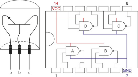 |
| Figure 7-1 Homogeneous—one or more identical parts in a package. |
Heterogeneous Parts
Figure 7-2 shows an example of a heterogeneous package. This package has three parts, which can be placed independently on the schematic: one relay coil (
K) and two sets of contacts (
A and
B). Although power can be applied to the coil and to one or more of the contacts, it is a passive device and does not have power pins (strictly speaking).
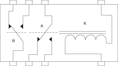 |
| Figure 7-2 Heterogeneous relay—dissimilar parts in a single package. |
Pins
When making parts in Capture that will be used to make a PCB design in PCB Editor or perform simulations in PSpice, one of the most important issues in making new parts is properly handling the pins. All the other lines that make up a part are cosmetic, but how the pins are assigned determines if you get design rule check errors when checking your schematic, if you have a PCB laid out correctly, and if a design simulates correctly.
There are eight types of pins. Each pin has a pin number, a pin name, and an order number. Each of these pins also has specific characteristics that determine how it performs in the package with regard to what it looks like in the schematic, how it is “judged” during design rule checks, how routing is governed in PCB Editor, and the like. Additionally, you can assign pin characteristics that determine what the pins look like once the part is placed into a schematic. Table 7-1 shows a summary of the pin types, shapes, and visibility options.
With regard to PCB layout, the pin types are simply power pins and nonpower pins (any of the other types). Power pins require special handling because of their global nature. For example, it needs to be considered if any of the pins will be shared between parts within one package, if they will be visible on all the parts, and if they will be connected to a global net or a nonglobal net. Examples that explain how to deal with pins are given later.
Part Editing Tools
The Select Tool and Settings
The Select tool is used to select pins, text, or any of the graphical objects (lines, arcs, etc.). You can select objects by clicking on them or dragging a box across or around objects (see the Area Select description).
The Snap-to-Grid function is actually a coarse or fine setting and never actually fully disables the snap-to functionality. If the Snap-to-Grid function is active (coarse setting), you can place or move objects only in 0.1-unit increments—this is the default. If the grid function is not active (fine setting), you can place or move objects in 0.01-unit increments. Except when working with graphics, the Snap to Grid should always be active.
Objects can be selected by fully enclosing the object with a selection box (using the Select tool) or just intersecting the object with the selection box. Using the fully enclose method is handy for selecting an object that is surrounded by many closely located objects.
When you move parts on your schematic, nets stay connected to the part and may cross over other nets or part pins may land on nets. Two modes of operation determine how these events change or allow connectivity. If the drag connect mode is off,
 , the default, then connectivity changes are prohibited. This helps prevent unwanted connections, but if you are placing new parts on the schematic, you need to specifically add new nets from existing nets to the new part to make connections. If the drag connect mode is active,
 , then connectivity changes are allowed. New or moved parts will automatically be connected to existing nets if the pins touch them. Red dots are used to indicate where connections will be made.
The Pin Tools
The Place Pin tool is used to place pins on a part one at a time.
The Array tool is used to simultaneously place multiple pins on a part, such as a 16-bit output port on a microcontroller. The Array tool enables you to establish a base name common to all the pins then automatically number each pin chronologically.
The Graphics Tools
PLACE IEEE SYMBOL

PLACE LINE TOOL

The Line tool is used to place a single orthogonal or diagonal line segment.
PLACE POLYLINE TOOL

The Polyline tool is used to place multisegment lines. Polylines are orthogonal by default but can be made diagonal by holding down the
Shift key on the keyboard while drawing the line.
PLACE RECTANGLE TOOL

The Place Rectangle tool is used to place closed rectangular parallelograms.
PLACE ELLIPSE TOOL

The Place Ellipse tool is used to place circles and ellipses.
PLACE ARC TOOL

The Place Arc tool is used to construct arcs and circles.
PLACE TEXT TOOL

The Place Text tool is used to place text objects, which have font, color, and rotation settings.
The Zoom Tools
ZOOM IN

The Zoom In tool zooms in by set increments. You can use the button, press the
I key on your keyboard, or select
Zoom In from the
View menu.
ZOOM OUT

The Zoom Out tool zooms out by set increments. You can use the button, press the
O key on your keyboard, or select
Zoom Out from the
View menu.
ZOOM TO REGION

Use this tool to zoom to a particular region of your design by dragging a box around the area to which you want to zoom.
ZOOM TO ALL

Use this tool to see the entire design.
Methods of Constructing Capture Parts
Four methods are used to construct Capture parts. Three of the methods are completed from the Capture Library Manager and the fourth is initiated from the PSpice Model Editor and finished with the Capture Library Manager. PCB footprints can be assigned to any of the parts regardless of how it was constructed, and the footprints can be assigned when the parts are first constructed or assigned later when the parts are actually used in a design.
Methods from Capture Library Manager:
1. Design menu → New part.
2. Design menu → New part from spreadsheet.
3. Tools menu → Generate part.
Method from PSpice Model Editor:
4.
File menu →
Export to Capture part Library (then use the Capture Library Manager to modify the part’s appearance).
Table 7-2 shows which method to use by how the part will be used. The procedure for each method is described later. Later in the chapter, it will be shown how to make and download PSpice models, which can be converted to Capture parts using Methods 3 and 4.
| Function/purpose of the part | Method of construction |
|---|---|
| Schematic entry only | Method 1 (easier) or Method 2 |
| Schematic entry and PCB layout | Method 1 (easier) or Method 2 |
| Schematic entry and PSpice simulation using functional OrCAD schematic designs (can also assign footprints for PCB layout) | Method 3 (easier) or Method 4 |
| Schematic entry and PSpice simulation using new or existing PSpice models (can also assign footprints for PCB layout) | Method 4 |
Method 1. Constructing Parts Using the New Part Option (Design Menu)
Constructing parts using the
New Part option in Capture is demonstrated through three design examples. The first two examples are used to design homogeneous parts; the first is a transformer (a single-part, passive device) and the second is an operational amplifier (a multipart, active device) with shared power pins. The third example is a heterogeneous, multipart, passive device.
DESIGN EXAMPLE FOR A PASSIVE, HOMOGENEOUS PART
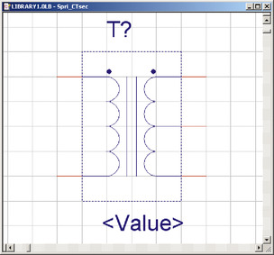
The first design example is of a transformer with an iron core, a single primary, and a center-tapped secondary. The transformer and its schematic representation are shown in Figure 7-3.
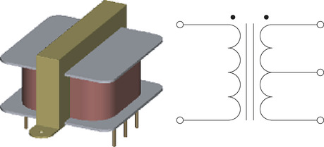 |
| Figure 7-3 Single-part, homogeneous transformer and schematic. |
To begin, start Capture and from the session frame navigate to
File→
New→
Library as shown in Figure 7-4.
 |
| Figure 7-4 Starting a new part from a new Capture library. |
The window that opens is the
Capture Library Manager. Select the
Library icon (Figure 7-5, left),then select
New Part from the
Design menu (Figure 7-5, right) or right click and select
New Part from the pop-up menu.
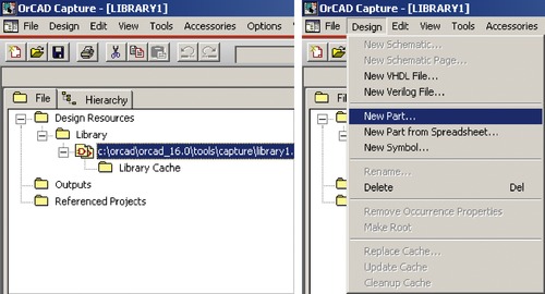 |
| Figure 7-5 Beginning a new part from the Library Manager. |
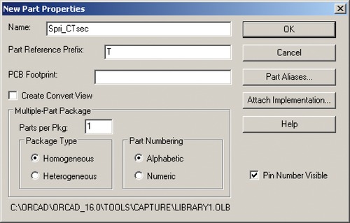
A
New Part Properties dialog box will open as shown in Figure 7-6. Enter a name for the part (for example, Spri_CTsec) and T for the reference prefix. You can also enter a PCB footprint if desired (or known). You can change this later if you are not sure what the footprint is or will be. Leave the
Parts per Pkg: as
1 and
Package Type as
Homogeneous. Select
Part Numbering as
Numeric and check
Pin Number Visible if you want the pin numbers to be visible on the schematic. Click
OK.
 |
| Figure 7-6 New Part Properties dialog box. |
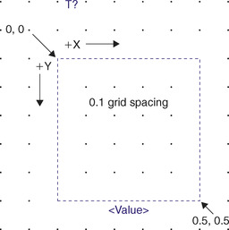
A part editing window will open with a dotted outline as shown in Figure 7-7. The dotted box defines the boundary of the part. Pins are placed on the boundary (as described later) and text and graphics are placed inside the boundaries. You can also add pictures and IEEE symbols if desired.
 |
| Figure 7-7 The new part shown in the part editing window. |
The default grid is 0.1×0.1
in., with the upper left corner as coordinate (0, 0). By default pins and graphical objects are placed on the grid. The snap-to-grid setting can be changed by toggling the Snap-to-Grid tool on,
 , or off,
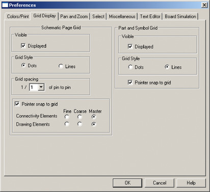
 . The grid can be shown as dots or lines. To make changes to the grid settings, navigate to
Options→
Preferences from the menu bar and select the
Grid Display tab as shown in Figure 7-8. Select the desired part and symbol grid properties on the right side of the dialog box.
. The grid can be shown as dots or lines. To make changes to the grid settings, navigate to
Options→
Preferences from the menu bar and select the
Grid Display tab as shown in Figure 7-8. Select the desired part and symbol grid properties on the right side of the dialog box.
| Snap to Grid:
On Off |
 |
| Figure 7-8 Grid settings in the
Options→Preferences dialog box. |
The first step to make the transformer is to make the part outline 0.4
in. wide by 0.6
in. tall (for comparison, resistors from the Analog library are 0.2×0.2
in., not including the pin lengths). To resize the part outline, left click on the dotted border then click to hold one of the corner squares (handles) and drag the corner to resize the box.
The next step is to add the pins that make the transformer’s five leads. To add pins to the part, toggle the pin tool,
 . The
Place Pin dialog box shown in Figure 7-9 will be displayed. Select
Short for the pin shape and
Passive for the pin type; click
OK. Place the first two pins on the left side of the border at positions (0.0, 0.1) and (0.0, 0.5) for the primary winding leads and three pins on the right side at positions (0.4, 0.1), (0.4, 0.3), and (0.4, 0.5) for the secondary winding leads. To quit placing pins press the
Esc key on the keyboard or right click and select
End Command from the pop-up menu.
. The
Place Pin dialog box shown in Figure 7-9 will be displayed. Select
Short for the pin shape and
Passive for the pin type; click
OK. Place the first two pins on the left side of the border at positions (0.0, 0.1) and (0.0, 0.5) for the primary winding leads and three pins on the right side at positions (0.4, 0.1), (0.4, 0.3), and (0.4, 0.5) for the secondary winding leads. To quit placing pins press the
Esc key on the keyboard or right click and select
End Command from the pop-up menu.
| Pin tool
|
 |
| Figure 7-9 The
Place Pin dialog box. |
The Place Pin tool will automatically increment the name and number of each pin as it is placed. To change a name or number of a pin, double click on a pin to bring up the
Pin Properties dialog box (which looks exactly like the
Place Pin dialog box) and change it as necessary. To simultaneously change the properties of multiple pins, hold down the
Ctrl key and left click each pin to select more than one pin. Then right click and select
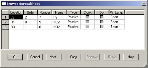
Edit Properties… from the pop-up menu. The
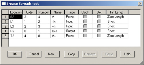
Browse Spreadsheet dialog box shown in Figure 7-10 will be displayed. More than one pin must be selected to get the spreadsheet, otherwise the
Pin Properties dialog box will be displayed.
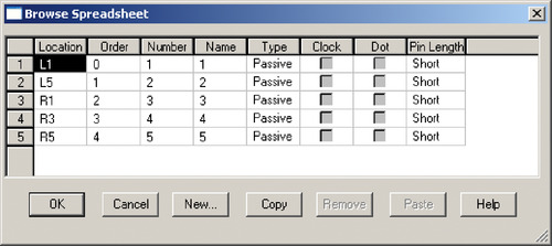 |
| Figure 7-10 Use the
Browse Spreadsheet dialog box to modify pin parameters. |
The pin type and pin length cells have dropdown lists that allow you to select the desired pin properties. The other columns require you to enter the values manually. The number and name are the same as the settings you can choose using the
Pin Properties dialog box. Naming pins is flexible, but the pin numbers you assign in a Capture part must match the pad name in a PCB Editor footprint. For PCB layout considerations, the pin order is irrelevant. The pin order is extremely important to PSpice, however, and is discussed in Methods 3 and 4.
The next step is to
place graphics to build the transformer coils. Turn the Snap to Grid off (toggle the grid button,
 , so that it turns red). Select the Place Arc tool,
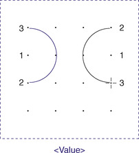
 . Arcs are defined by three points, as shown in Figure 7-11. The first point you click defines the center of the arc, the second point defines where the arc starts, and the third point defines the end. The arc is drawn counterclockwise from point 2 to point 3, so the location of point 2 depends on the direction you want the arc to face. After you have placed the first couple of arcs, you can copy and paste the rest in place.
To copy graphic objects, toggle the Select tool,
. Arcs are defined by three points, as shown in Figure 7-11. The first point you click defines the center of the arc, the second point defines where the arc starts, and the third point defines the end. The arc is drawn counterclockwise from point 2 to point 3, so the location of point 2 depends on the direction you want the arc to face. After you have placed the first couple of arcs, you can copy and paste the rest in place.
To copy graphic objects, toggle the Select tool,
 , and select the objects you want to copy. Left click once to select a single object or use
Ctrl+left click to select multiple objects.
Copy and
Paste the objects as will be shown in Figure 7-13 using typical Windows Copy/Paste techniques. You can also left click once to select an object, then hold down the
Ctrl key, left click and hold the part and “drag a duplicate part” out of the first, release the mouse button to place the copy, then release the
Ctrl key.
, and select the objects you want to copy. Left click once to select a single object or use
Ctrl+left click to select multiple objects.
Copy and
Paste the objects as will be shown in Figure 7-13 using typical Windows Copy/Paste techniques. You can also left click once to select an object, then hold down the
Ctrl key, left click and hold the part and “drag a duplicate part” out of the first, release the mouse button to place the copy, then release the
Ctrl key.
| Grid button
|
| Place Arc tool
|
| Select tool
|
 |
| Figure 7-11 Making coils with the Place Arc tool. |
Next, place two parallel lines between the arcs to represent the core. Use the Place Line tool,
 , to draw them. Then make the dots for the dot–coil indicator by using the Place Ellipse tool,
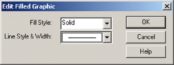
 . Draw a small circle near one of the coils, then hit the
Esc key to exit drawing mode. Change the circle to a filled dot by using the
Edit Filled Graphic dialog box shown in Figure 7-12. To display the dialog box, use the Select tool to select the circle then right click and select
Edit Properties from the pop-up menu. You can leave the
Line Style as is but change the
Fill Style to
Solid. Click
OK
. Draw a small circle near one of the coils, then hit the
Esc key to exit drawing mode. Change the circle to a filled dot by using the
Edit Filled Graphic dialog box shown in Figure 7-12. To display the dialog box, use the Select tool to select the circle then right click and select
Edit Properties from the pop-up menu. You can leave the
Line Style as is but change the
Fill Style to
Solid. Click
OK
.
| Place Line tool
|
| Place Ellipse tool
|
 |
| Figure 7-12 Use the
Edit Filled Graphic dialog box to fill objects with patterns. |
Figure 7-13 shows the transformer design so far. Note that the pin numbers are on the pin outside the boundary and pin names are inside the boundary with the graphics.
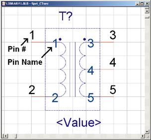 |
| Figure 7-13 Completed part with pin names and numbers visible. |
You can
use theUser Propertiesdialog box to change the visibility of the pin names and numbers, shown in Figure 7-14 (left). To display the
User Properties dialog box, select
Part Properties from the
Options menu. Use the
User Properties dialog box to make the pin names and numbers invisible. You can also change the visibility of the pin numbers using the check box in the
Edit Part Properties dialog box shown in Figure 7-14 (right).
To display theEdit Part Propertiesdialog box, select
Package Properties from the
Options menu. The completed part is shown in Figure 7-15.
 |
| Figure 7-14 User Properties dialog box from Options → Part Properties menu: (left) User Properties dialog box (Part Properties), (right) Edit Part Properties dialog box (Package Properties). |
 |
| Figure 7-15 Completed homogeneous part (pin names and numbers not visible). |
The final task is to save the new part (and the library if it is new).
To save the part, close the part editing window and click
Yes at the
Save changes to partname? prompt.
To save the library, select the
Library icon in the Project Manager, right click, and select
Save As… from the pop-up menu. Save the library with a new name in your
UserLibrary in the
Capture/Library path.
DESIGN EXAMPLE FOR AN ACTIVE, MULTIPART, HOMOGENEOUS COMPONENT
The second example shows how to construct the dual op-amp component shown in Figure 7-16. The parts are identical (homogeneous) and share the power pins.
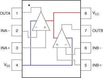 |
| Figure 7-16 Data-sheet diagram for a dual op-amp component. |
Begin as you did with the transformer, by selecting
New Library from the
File menu in the Capture session frame. Select the
Library icon in the Library Manager, right click, and select
New Part from the pop-up menu. In the
New Part Properties dialog box (Figure 7-17), enter a name for the op amp, make
U the part reference prefix, and change the parts per package to 2. Leave the package type as homogeneous, assign alphabetic part numbering, and make the pin numbers visible. Click
OK when you are finished.
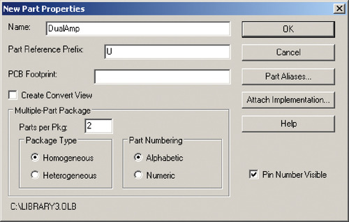 |
| Figure 7-17 New Part Properties dialog box for a dual op amp. |
Use the Place Pin tool to begin placing pins as shown in Figure 7-18. Label and place pins for part A per the data sheet (Figure 7-16). You can either correctly name and number each pin as you place it or place all the pins then go back and fix the names and numbers after they have been placed. Whichever method you use, set the pin characteristics as shown in Figure 7-19. Remember that, to change a name or number of a pin, double click on a pin to bring up the
Pin Properties dialog box and, to change the properties of multiple pins simultaneously, hold down the
Ctrl key and left click each pin to select more than one pin. Then right click and select
Edit Properties… from the pop-up menu. Finally, add short graphic lines between the op-amp body and the power pins using the
Place Line tool,
 . You may need to turn off the
Snap to Grid to do this. Remember to turn the
Snap to Grid back on when you are finished with the graphics.
. You may need to turn off the
Snap to Grid to do this. Remember to turn the
Snap to Grid back on when you are finished with the graphics.
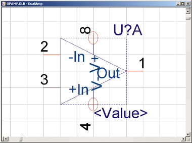 |
| Figure 7-18 Dual op amp, part A. |
 |
| Figure 7-19 Pin characteristics for part A of the dual op amp. |
In the
Part Editing window, make the part border 0.4×0.4
in. Then make the triangular body of the op amp using the Place Line tool (see Figure 7-18).
| Place Line tool
|
As you can see from Figure 7-18, the op amp looks cluttered because the pin names run into each other and are not optimally spaced with respect to each of the pins. You can fix this by making the pin names
not visible and adding your own text. First,
turn the pin names off by setting the
Pin Names Visible to
False in the
User Properties dialog box (from the
Options → Part Properties menu). Use the Place Text tool or the Place Line tool to add−and+signs in place of the −IN and +IN pin names. Add text near the power pins to indicate which is the positive supply pin and which is the negative supply pin.
For the time being, that completes part A. There are a couple of ways to get to part B.
To view a specific part of a multipart device, go to the
View menu and select
Package to see both parts, as shown in Figure 7-20. Then double click on part
U?B. Alternatively you can select
Next (or
Previous)
Part from the
View menu, or use
Ctrl+N or
B on your keyboard to toggle through the parts.
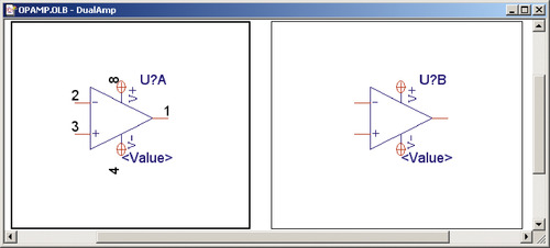 |
| Figure 7-20 Package view of dual op-amp part. |
Once you have part B in the editing window, select all of the pins and set the parameters as shown in Figure 7-21 using the procedure described previously.
 |
| Figure 7-21 Pin characteristics for part B of the dual op amp. |
ASSIGNING POWER PIN VISIBILITY
If you compare Figure 7-19 to Figure 7-21, you see that parts A and B share pins 4 and 8. Shared power pins require special handling to make the parts look and function properly between Capture, PSpice, and PCB Editor. The type and visibility of shared pins can be power and visible, power and nonvisible, or nonpower and visible. Digital parts usually share nonvisible power pins, while active analog parts typically share either visible power pins or nonpower-type pins (such as input or passive pins), which are always visible. The type and visibility are initially established at the part level in the library, but you can change these parameters at the schematic level after you have placed the part into your design.
Several methods can be used for changing the part properties on the schematic, and each method has slightly different effects. If you add up all the combinations of the possible pin settings with the various methods of setting them, you will find over 200 possible combinations! Some of the combinations can cause severe errors that prevent you from creating netlists, others cause various types of warnings, and still others cause no errors or warnings but fail to route correctly on the board. We do not discuss all 200 combinations here, but we look at various scenarios in the PCB Design Examples. For now, to keep things simple and to follow typical convention, we make the shared power pins visible power pins since this is an analog part.
To set a power pin’s properties, select pin 8 then right click and select
Properties from the pop-up menu (or just double click the pin) to bring up the
Pin Propertiesdialog box (see Figure 7-9 for an example). Make sure that the
Pin Visible box is checked, an option that is available only for power pins (since all other types of pins are always visible). If you use the
User Properties dialog box (
Options→Part properties), you can set the visibility of only the pin’s names or numbers, not the visibility of the pin itself. The completed op amps are shown in Figure 7-22. Save the parts as described previously.
 |
| Figure 7-22 The finished op amps. |
When you use a part with shared pins in a schematic then create a PCB Editor netlist, you may get the warning,
WARNING [MNL0016] Duplicate pin number ‘4’ on ‘LM324’. If the part was constructed properly, you can ignore the warning.
DESIGN EXAMPLE FOR A PASSIVE, HETEROGENEOUS PART
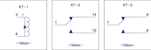
In this design example we make a passive, heterogeneous part, namely, a double-pole, double-throw relay, as shown in Figure 7-23. The relay consists of three parts: two sets of identical double-throw contacts and an operating coil with its clamping diode.
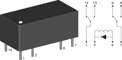 |
| Figure 7-23 A heterogeneous, multipart relay: (left) relay package, (right) relay schematic. |
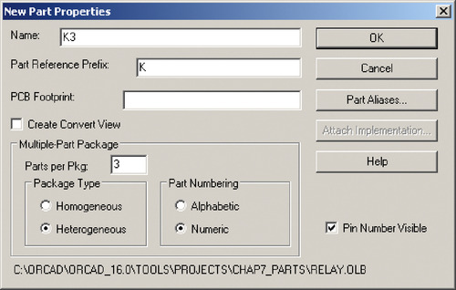
Begin by navigating to
File → New → Library from the Capture session frame as described in the preceding examples. Select the
Library icon and select
New Part from either the
Design menu or the pop-up menu after right clicking on the icon. Fill out the
New Part Properties dialog box as shown in Figure 7-24. Make sure you select
3 parts per package and select the heterogeneous package type. Click
OK. From the
View menu, go to the
Package view to make sure that you have three parts.
 |
| Figure 7-24 New Part Properties dialog box for the heterogeneous relay. |
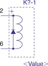
Begin by constructing the relay coil and clamping diode as part
K?-1. Bring up
K?-1 in an editing window; double click on the
K?-1 window if you are in the
Package view or use
Ctrl+N on your keyboard to toggle through the parts if you are in the
Part view. Resize the border so that it is 0.3
in. wide by 0.6
in. tall. Using Figure 7-25 as a guide, use the Place Pin tool to place two pins on the left side of the part border. Define the top pin as number 2 with name C1 and the bottom pin as number 6 with name C2. Make both pins short, passive lines, and make the names nonvisible. Use the Place Line and Place Arc tools to add the coil, diode, and “1” graphics to the part as described in the previous examples.
 |
| Figure 7-25 Relay coil and diode. |
The next step is to add the first set of contacts. Toggle to part
K?-2. Resize the border to 0.4
in. wide by 0.6
in. tall. Using Figure 7-26 (left) as a guide, add two pins to the right side of the border and one on the left. Set the pin parameters as shown in Figure 7-26 (right), and make the pin names nonvisible. Use the Place Line tool to add the pole and the lines leading from the pin to the throws (the contacts).
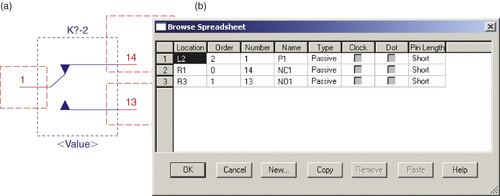 |
| Figure 7-26 Schematic (left) and pin settings (right) for the first set of relay contacts. |
Use the Place Polyline tool to draw the throws so that you can make them solid filled. Use the
Shift key to make diagonal polylines. After you have the triangle drawn, double click on it to bring up the
Edit Filled Graphic dialog box and set the fill to
Solid.
Once you have the pole and throws for contact assembly
K?-2 finished, copy and paste the graphics into the
K?-3 part. To copy all the pieces at one time, hold down the
Ctrl key on your keyboard and select each line and polyline one at a time. Once you have them all selected, right click and select
Copy from the pop-up menu (or select
Copy from the
Edit menu or use
Ctrl+C on your keyboard). Go to the next part,
K?-3, by typing
Ctrl+N on your keyboard then paste the copied graphics into the empty part outline (right click and select
Paste from the pop-up menu, select
Paste from the
Edit menu, or use
Ctrl+V on your keyboard). Add three pins using the Place Pin tool as you did for the previous parts. Set the pin parameters as shown in Figure 7-27. You will notice that the order starts at 0 for each part. The order of the pins is of concern only when the part is to be used with a PSpice model for performing simulations. We address that issue in the next sections. The completed, multipart relay is shown in Figure 7-28.
 |
| Figure 7-27 Pin parameters for the second set of contacts. |
 |
| Figure 7-28 Package view of the completed heterogeneous relay. |
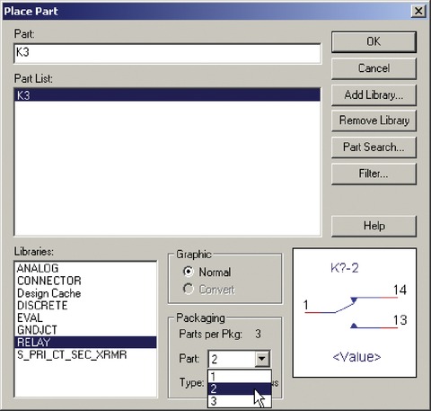
When you place the relay in a Capture schematic, use the
Part: dropdown list as shown in Figure 7-29 to place the desired part of the multipart package.
 |
| Figure 7-29 Selecting a part from a multipart package in a Capture schematic. |
Method 2. Constructing Parts with Capture Using the Design Spreadsheet
Use this method to automatically generate a single or multipart package. It is similar to the first method, except that you define all the pins up front, using the spreadsheet shown in Figure 7-30.
New Part from Spreadsheet generates heterogeneous packages by default, but you can use it to make homogeneous parts. The parts will be defined as heterogeneous but will be homogeneous in effect if there are no differences between the parts.
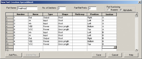 |
| Figure 7-30 The New Part Creation Spreadsheet. |
To construct a part using the design spreadsheet, open an existing Capture library to which you want to add a part, or start a new library as described previously. In the Library Manager, select the
Library icon and select the
New Part from Spreadsheet… option, which you can do either from the
Design menu or from the pop-up menu by right clicking on the
Library icon.
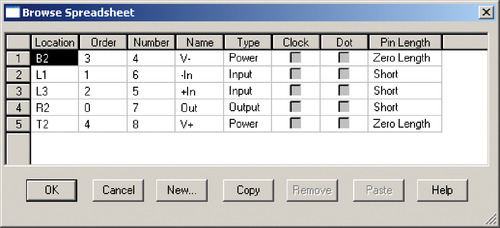
The spreadsheet will initially be blank. Add the pin numbers and parameter settings as needed per the part requirements. The pin settings shown in Figure 7-30 would generate a part identical to the dual op amp designed in a previous example (see Figure 7-16).
Notice that pins 4 and 8 were added twice, once for each part, to define the shared power pins.
After the pin parameters have been entered into the spreadsheet, click the
Save button. The information box shown in Figure 7-31 will be displayed, letting you know that there were warnings (because of the duplicate pins). You can view the warnings or click
Continue to view the parts.
 |
| Figure 7-31 New Part Creation warnings. |
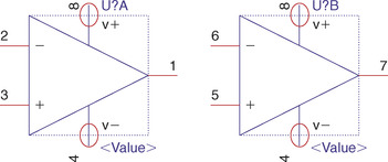
Figure 7-32 shows the package view of the parts generated by the spreadsheet. By default, the “parts” are initially represented by simple boxes. All you have left to do at this point is to modify the graphics to make the op amps cosmetically correct. In the homogeneous op amp from the previous example, all parts were automatically made identical when you made a graphic in one part. Since this is a heterogeneous part by default (which you cannot change), you have to modify the graphics on every part individually. Delete the boxes that lie on top of the dotted outline and add the graphics as described in the previous op-amp example.
 |
| Figure 7-32 Package view of new parts generated using the spreadsheet. |
Method 3. Constructing Parts Using Generate Part from the Tools Menu
Use this method to create a new Capture part (or parts) from a PSpice model library or a Capture project. The part(s) can then be used for schematic entry, PSpice simulations, and PCB layout (if you assign a footprint to it). To use this method, a PSpice model library or a functional schematic design needs to preexist. In the section that follows, several methods for developing or obtaining the PSpice libraries and functional schematic designs are described. For the time being we will go ahead under the assumption that a PSpice library is available so that the part creation process is kept separate from the library/schematic creation process.
Begin by starting a new Capture library or open an existing library from the Capture session frame’s
File menu. Select the
Library icon and then select
Generate Part… from the
Tools menu. The
Generate Part dialog box will pop up, as shown in Figure 7-33.
 |
| Figure 7-33 Generate Part dialog box from the
Tools menu. |
Select
PSpice Model Library (or
Capture Schematic/Design if appropriate) from the
Netlist/source file type: list, then select the library (*.lib etc.) or design (*.dsn etc.) from the
Netlist/source file: list. Make sure that the
Destination part library: path and name are what you want and that the library has a .OLB extension. Make sure that the
Create new part option is checked and click
OK.
After Capture has completed importing the library/design file you selected, you should see the list of parts in the Library Manager. If the Capture library (.olb) you are working with was originally empty, the new parts will be located directly under the
Library icon in the
Design Resources folder. But if the library already had some parts in it, the new parts and copies of the previously existing parts will be added to both the
Library icon and the
Library folder under the
Design Resources folder (see Figure 7-34, in which, as an example, the breakout library was added to the
analog_p library). The
Library folder will also contain a duplicate of the
Library icon. This allows you to copy, add, or delete parts to or from the new library. Once you are satisfied with which parts are contained under the
Library icon under the
Design Resources folder, you can delete the duplicate
Library icon and parts in the
Library folder, keeping just the library in the
Design Resources folder.
 |
| Figure 7-34 Structure of Library Manager after copying a library into an existing library. |
Once you finish adding parts to the library, you can edit the added part(s), pins, and links to footprints using the Capture Part Editor, and the
Part and
Package properties dialog boxes from the
Design menu as described in previous examples.
Finally, save and close the library. You can now use the library and its parts in new designs for schematic entry, simulations, and PCB layout.
Method 4. Generating Parts with the PSpice Model Editor
You can use the PSpice Model Editor to make Capture parts that can be used in schematic designs, circuit simulations, and PCB layouts. The difference between using the PSpice Model Editor and the
Generate Part method (Method 3) is that you can work directly on and with the PSpice models with the Model Editor.
Start the PSpice Model Editor. Go to
Start→All Programs→OrCAD 16.0→PSpice Accessories→ . You will begin with a blank
Model Editor session window.
To open an existing PSpice library (
name.LIB), navigate to
OrCAD/tools/pspice/library and select
Open from the
File menu. Select one of the libraries (e.g.,
bipolar.lib) and click
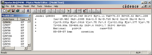
Open; then select one of the models from the model list. Figure 7-35 shows the Q2N696 BJT transistor model from the
bipolar library. The
Models List window pane shows all of the simulation models contained in the library, and it tells you whether it is a primitive model or a subcircuit model. The text window to the right of the
Models List displays the “code” that describes the model.
. You will begin with a blank
Model Editor session window.
To open an existing PSpice library (
name.LIB), navigate to
OrCAD/tools/pspice/library and select
Open from the
File menu. Select one of the libraries (e.g.,
bipolar.lib) and click
Open; then select one of the models from the model list. Figure 7-35 shows the Q2N696 BJT transistor model from the
bipolar library. The
Models List window pane shows all of the simulation models contained in the library, and it tells you whether it is a primitive model or a subcircuit model. The text window to the right of the
Models List displays the “code” that describes the model.
| PSpice Accessories
|
 |
| Figure 7-35 A PSpice library as viewed from the Model Editor. |
You can construct new models by using existing model listings as examples and/or the model descriptions found in the PSpice reference guide (
pspcref.pdf) located in the
OrCAD/doc folder. The following sections describe how to download primitive models (models beginning with .model) from the Internet and how to create your own subcircuit models (models beginning with .subcircuit). The models can then be added to a PSpice library from which you can generate Capture part libraries as described. Creating custom primitive models is not described here.
GENERATING A CAPTURE PART LIBRARY FROM A PSPICE MODEL LIBRARY
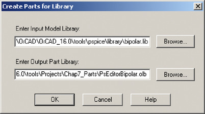
Beginning with a PSpice library (.lib) open in the Model Editor (similar to Figure 7-35), select
Export to Capture Part Library… from the Model Editor’s
File menu. You will be presented with the
Create Parts for Library dialog box shown in Figure 7-36. In the
Enter Input Model Library: text box, use the
Browse… button to find the PSpice library (*.LIB) for which you want to make parts. Use the second
Browse… button to specify the location for the new Capture library (*.OLB). Remember that the PSpice models and the libraries that contain them are usually stored in the
OrCAD/tools/pspice/library path, while the Capture parts that use the models are stored in the
…OrCAD/tools/capture/libraries/pspice path. Click
OK once you have the input and output libraries and paths specified.
 |
| Figure 7-36 The PSpice
Create Parts for Library dialog box for Capture parts. |
Note: A Capture part library (
bipolar.olb) already exists in the
Tools/Capture/Library/PSpice folder for the
bipolar PSpice model library (
bipolar.lib). The
bipolar library is used here for demonstration purposes. If you perform the following procedure on an existing library, save the new library to a temporary or user folder so that you do not overwrite the existing library.
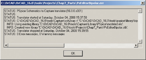
When the Model Editor has finished, it will display an information box similar to the one in Figure 7-37. If the Model Editor is successful at generating the Capture part library, the last line will say
0 Error messages, 0 Warning messages. Click
OK to close the information box.
 |
| Figure 7-37 New part creation information box. |
The PSpice Model Editor generates Capture parts with correctly named and numbered pins, but the parts are generic boxes because the PSpice Model Editor describes only how the parts function, not what they look like. You need to use the Capture Part Editor to modify the graphical appearance of the parts, as described in the earlier examples. To view the new part library, start Capture and select
Open→Library… from the
File menu in the Capture session frame.
MAKING AND/OR OBTAINING PSPICE LIBRARIES FOR MAKING NEW CAPTURE PARTS
Before you send a final board design to be manufactured, at some point in the design process you will want to simulate your design. A detailed explanation of PSpice model development and simulation process is outside of the scope of this text and many references are available on the subject. But in the interest of completeness, a brief explanation of how to add PSpice models to your Capture parts is discussed here.
PSpice contains many libraries, but manufacturers continually design new parts, which may not be included with your version of PSpice, so eventually you will want to be able to develop your own Capture parts that have simulation capabilities (and ultimately will be used in a board design).
A PSpice library contains primitive models (such as resistors and diodes) and subcircuit models (such as logic gates and op amps). Primitive models are basically limited to behavioral descriptions of single devices. Subcircuit models can describe the behavior of a single device, multiple devices, or complete circuit designs. Unless specifically noted,
model in this text refers to both primitive and subcircuit models in general.
With regard to PSpice model libraries, the models that the libraries contain begin as simple text files that have a .mod extension. A model is added to a library by importing it into the PSpice (.lib) library. Once the model is imported into the library, the original .mod file is no longer needed and can be deleted or archived in a separate folder.
DOWNLOADING LIBRARIES AND/OR MODELS FROM THE INTERNET
The easiest way to make a new PSpice model library is to download it from the manufacturer’s Web site (when available). You can often download complete libraries, but sometimes OEMs provide only individual models that you can add to your own libraries.
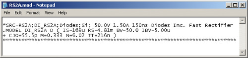
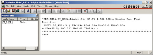
Here is an example. Suppose you were to use an RS2A fast recovery diode (Diodes Incorporated) in your design and need its PSpice model. By going to the Diodes Incorporated Web site (www.diodes.com/products/spicemodels/index.php), you can obtain the model for the RS2A diode as shown in Figure 7-38. Copy the text as is from the Internet Explorer window and paste it into any simple text editor such as Notepad. Save the text file with a .mod file extension (e.g., RS2A.mod) to a convenient folder that is set up for your collection of model files.
 |
| Figure 7-38 Spice diode model downloaded from the Web. |
Next start a new PSpice library for Diodes Incorporated parts. From the PSpice Model Editor
File menu choose
New. You will be presented with a blank
Models List window pane and an unsaved library (
Untitled1.lib). From the
Model menu, choose
Import. From the
Open File dialog box, navigate to and select the
RS2A.mod file. Click
Open. The
Models List window should now contain the new model as shown in Figure 7-39. Save the new library in a user folder with a name such as
DiodesInc.lib (select
Save As… from the
File menu). You now have a PSpice library (with only one part in this case) for which you can make a new Capture part. To make a Capture part for the new library, use the
Export to Capture Part Library… command from within the PSpice Model Editor as described under Method 4 or use the
Generate Part command from within Capture as described under Method 3.
 |
| Figure 7-39 New RS2A PSpice model in the Model Editor. |
MAKING A PSPICE MODEL FROM A CAPTURE PROJECT
In the event that a PSpice model (or even a generic spice model) cannot be located, you can make your own *.mod file. There are two ways to do this, depending on the type of model you are trying to make. If you need to make a primitive model for a device (e.g., a diode or P-channel MOSFET transistor), you need to compose a .mod file using a text editor then import the model into a library as just described. To make an accurate model, you need to be familiar with model parameters for the part and the “code” that PSpice understands. This is not described here, but you can read about the details in the PSpice Reference document (
pspcref.pdf) located in the
OrCAD/doc folder. As a starting point you can also look at examples from the PSpice Breakout library (
breakout.lib).
If you need to make a model for a nonprimitive part (an IC or a transformer, for example), you can compose a subcircuit model without having extensive knowledge of model parameters or PSpice code. You simply “draw” the circuit using Capture, have Capture write the subcircuit model for you, then save it as a PSpice library. Once you have the .LIB file, you can use Method 3 or 4 to make a Capture part with the model attached to it and attach a PCB Editor footprint if so desired.
An example of how to make a PSpice model and subsequent Capture part is given here for a transformer with a single primary winding and a center-tap secondary, similar to the one in Figure 7-3 (except that the transformer in this example has a PSpice model—a PSpice template—associated with it). Using this procedure you can specify the inductance and DC resistance of the windings and the coupling between the windings for a specific part as described in a data sheet.
The basic process is as follows:
1. Use Capture to draw a circuit that you can simulate. The circuit will consist of inductors, resistors, and coupling coefficients.
2. After the transformer “circuit” is simulated to verify it behaves correctly, simulation sources are deleted and hierarchical ports are added to the schematic, which will become the leads (pins) of the transformer.
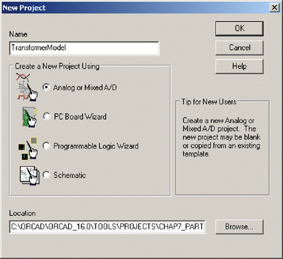
To make a .subcircuit model, open Capture and choose
New → Project… from the session frame’s
File menu. From the
New Project dialog box, choose
Analog or Mixed A/D as shown in Figure 7-40.
 |
| Figure 7-40 New Project dialog box for a PSpice project. |
Select the location of the new project using the
Browse… button at the bottom of the dialog box. If you plan on making more models in the future, it is a good idea to create a new folder just for model development. Once you have your models fully developed and tested, you can copy the finished libraries into the normal Capture and PSpice library folders.
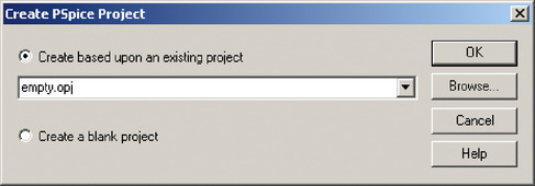
After you click
OK, the
Create PSpice Project dialog box (Figure 7-41) will be displayed. Check the
Create based upon an existing project radio button and select either the
empty.opj or the
simple.opj project template. Different templates may be displayed depending on which version you have. For what we are going to do in this example, it really does not matter which template you start with. Click
OK.
 |
| Figure 7-41 The
Create PSpice Project dialog box. |
In the Project Manager window, expand the
Design (.dsn) icon if it is not already expanded, and double click the
SCHEMATIC1 folder (see Figure 7-42). The name of the design (
DesignName.dsn) will become the default name of the PSpice library (
DesignName.lib), and the name of the root folder (
FolderName) will become the name of the PSpice part model (
.subcircuitFolderName…), so you want to change the name of the folder from
SCHEMATIC1 to the name you wish for your part.
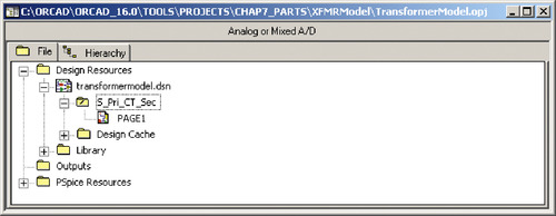 |
| Figure 7-42 Project Manager view of design. |
To rename the schematic folder, select the folder by left clicking once, then right click, and select
Rename from the pop-up menu. Change the name of the schematic folder to the name that you want the part to have (e.g.,
S_Pri_CT_Sec for single-winding primary, center-tap secondary).
Double click on the
PAGE1 icon to display the schematic page (see Figure 7-42). Delete any parts or text provided by the template by dragging a box around (or across) the parts to highlight them, then hit the
Delete key on your keyboard.
Place four resistors from the
Analog library (which have PSpice models associated with them) on the schematic page (see Figure 7-45 later). The resistors are used to simulate the DC resistance of the windings and a dummy load resistor. You can get the resistors from the
Place Part dropdown list located on the toolbar at the top of the window frame or by selecting the
Place Part button,
 , on the toolbar at the right of the schematic page. If you use the
Place Part button, you will be presented with the
Place Part dialog box shown in Figure 7-43. Select
ANALOG from the
Libraries: list then scroll down the
Part List: and select part
R. Notice that the parts in the
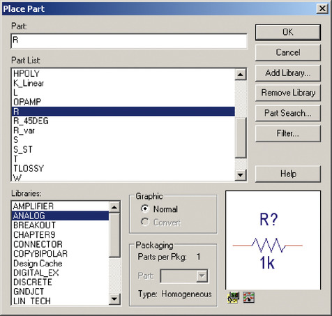
Analog library have PSpice models and footprints associated with them, as indicated by the PSpice and Layout (not PCB Editor) icons located under the part preview box in the lower right corner of the dialog box. Click
OK. Click on the schematic page in four places to place four resistors (see Figure 7-45 later for reference).
, on the toolbar at the right of the schematic page. If you use the
Place Part button, you will be presented with the
Place Part dialog box shown in Figure 7-43. Select
ANALOG from the
Libraries: list then scroll down the
Part List: and select part
R. Notice that the parts in the
Analog library have PSpice models and footprints associated with them, as indicated by the PSpice and Layout (not PCB Editor) icons located under the part preview box in the lower right corner of the dialog box. Click
OK. Click on the schematic page in four places to place four resistors (see Figure 7-45 later for reference).
| Place Part button
|
 |
| Figure 7-43 Place Part dialog box. |
Repeat this procedure to place three inductors (part
L) on the schematic page. One inductor serves as the primary winding, and the other two serve as the secondary windings. The inductors will be used to define the inductance (the turns ratios) of the primary and secondary windings.
Next, place one
K_Linear part from the
Analog library on the schematic page.
K_Linear defines the coupling coefficient of the windings.
Place a
VSIN part on the schematic page so that we can test the operation of the transformer. VSIN is located in the
SOURCE library.
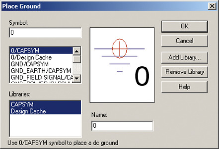
Finally, place three zero (0) ground references on the schematic page. Click the
Place Ground tool,
 , then select
0/SOURCE from the
Place Ground dialog box, as shown in Figure 7-44. For schematic entry and PCB Editor, you can use any ground symbol, but for PSpice simulations you have to have at least one 0 reference ground.
, then select
0/SOURCE from the
Place Ground dialog box, as shown in Figure 7-44. For schematic entry and PCB Editor, you can use any ground symbol, but for PSpice simulations you have to have at least one 0 reference ground.
| Place Ground tool
|
 |
| Figure 7-44 Place Ground dialog box. |
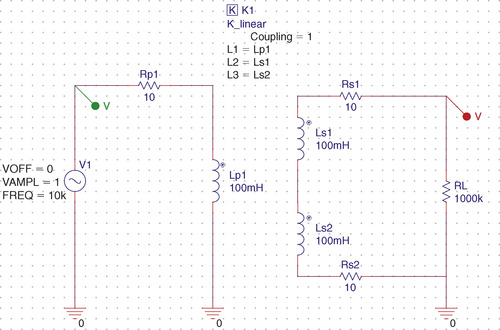
Position and rename the components, wire the circuit, and change the values of the components as shown in Figure 7-45. To change the reference designators (e.g., R1 or Rp) or the component values (e.g., 10
Ω), double click the property you want to change. In the
Display Properties dialog box, enter the appropriate value and click
OK.
 |
| Figure 7-45 Schematic of the linear step-up transformer. |
You can also modify a part’s properties by double clicking the part (or click once to select it then right click and select
Edit Properties… from the pop-up menu). A
Property Editor spreadsheet will pop up, as shown in Figure 7-46. If the properties are listed across in rows instead of vertically in columns, you can change the view by selecting the upper left-hand (corner) cell to highlight the entire spreadsheet, then right click and select
Pivot from the pop-up menu. You can also specify how many items are listed by using the Filter by: dropdown list just above the spreadsheet cells. To display all pertinent properties, select the
<Current properties> option located at the top of the list.
 |
| Figure 7-46 Part Property Editor spreadsheet (vertical view). |
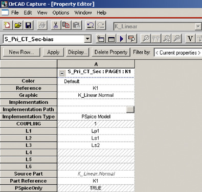
To modify and display the
K_Linear coupling properties, double click the coupling part to bring up the spreadsheet. Make sure that either the
Current properties or the
OrCAD-PSpice filter option is selected. In the L1 cell, type
Lp1 (or whatever you named your primary coil) then click the
Display button, which is located just above the spreadsheet cells. Enter
Ls1 in the L2 cell and
Ls2 in the L3 cell and click the
Display button for both of these parameters too. The L1, L2, and so on cells establish which coils are coupled as part of the transformer. You can have additional or separate coupling coefficients for different sets of coils, but for this example we have all three equally coupled together using the single linear coupler. Once you finish, close the spreadsheet by clicking the
X button in the upper right-hand corner of the spreadsheet.
Now we need to simulate the part with PSpice. You can perform several types of simulations with PSpice. In this example we perform a time domain analysis so that we can see the AC waveforms at the input of the transformer and at the load resistor.
To test the circuit we need to set up a simulation profile.
To set up a simulation profile, choose
Edit (or
New)
Simulation Profile from the
PSpice menu. In the
Simulation Settings dialog box (see Figure 7-47), select the
Analysis tab. In the
Analysis type: dropdown list, select
Time Domain (Transient). Set the rest of the parameters as shown in Figure 7-47, then click
OK.
 |
| Figure 7-47 Simulation Settings dialog box. |
Place voltage markers on the circuit to specify which voltages to display in the PSpice probe window. Click the Voltage Probe button,
 , on the toolbar and place a probe on the wire coming from VSIN (green marker) and one (red marker) on the wire going from the secondary winding to the load resistor (RL).
| Voltage Probe Button
|
Start the simulation by clicking the
Run PSpice button,
 . PSpice runs the simulation and displays the results in a probe window, as shown in Figure 7-48.
The voltage curves show that the transformer functions as a 1:2 step-up transformer, since the output (red marker curve) is twice as high as the input (green marker curve). Additional tests (e.g., frequency response) could be performed to validate the circuit model further, but these are not discussed here.
| Run PSpice button
|
 |
| Figure 7-48 PSpice probe window for the center-tap transformer. |
Since the circuit model has been validated, we now prepare to make a PSpice model of the circuit. Begin by deleting the VSIN source, the load resistor RL, and all the ground references.
Add ports to the schematic, which will serve as the leads of the transformer. Click the Place Port tool,
 . Select the
PORTBOTH-L port from the
Place Hierarchical Port dialog box, as shown in Figure 7-49. All the port symbols behave identically in Capture, PSpice, and PCB Editor. The only difference is the appearance on the schematic. Since the transformer is a passive device, we use the symbol that indicates that an applied signal can go in either direction. Click
OK and place five of the ports on the schematic page (two for the primary and three for the secondary).
. Select the
PORTBOTH-L port from the
Place Hierarchical Port dialog box, as shown in Figure 7-49. All the port symbols behave identically in Capture, PSpice, and PCB Editor. The only difference is the appearance on the schematic. Since the transformer is a passive device, we use the symbol that indicates that an applied signal can go in either direction. Click
OK and place five of the ports on the schematic page (two for the primary and three for the secondary).
 |
| Figure 7-49 Place Hierarchical Port dialog box. |
Reposition, connect, and label the ports as shown in Figure 7-50.
| Place Port tool
|
 |
| Figure 7-50 Hierarchical ports in the circuit design. |
Display the
Project Manager window by minimizing the schematic page or
ProjectName.opj from the
Window menu. Select the
Design icon then select
Create Netlist from the
Tools menu.
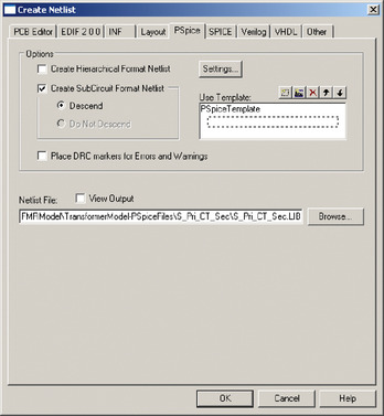
In the
Create Netlist dialog box (Figure 7-51), select the
PSpice tab. Check the
Create SubCircuit Format Netlist box and the
Descend radio button. A default name will be given to the netlist. Modify the path and name as desired. Make sure the name ends with the .LIB file extension. Click
OK.
 |
| Figure 7-51 Create Netlist dialog box. |
You now have a PSpice library file with one model (the transformer) in it. You can use Method 3 or 4 to generate a Capture part library from this model or add it to an existing part library. To complete the example we use Method 4 so that we can take a look at the PSpice model generated by Capture.
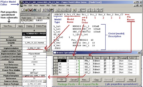
Start the PSpice Model Editor again. From the
File menu, select
Open and navigate to the transformer library that you made previously. Click on the
S_Pri_CT_Sec model to display the model in the editing window, as shown in Figure 7-52. Notice that the model type is .SUBCKT (a subcircuit). The name of the library is whatever you specified as the netlist file in the
Create Netlist dialog box, and the name of the part is the schematic folder name in the Capture design (see Figure 7-42). At this point you could modify the part to add specific requirements that will carry forward into the Capture part. Once the model editing (if any) is completed, generate the Capture part as described previously, using Method 3 or Method 4.
 |
| Figure 7-52 PSpice transformer model generated from a Capture project. |
Note that, as shown in Figure 7-52, the pin names and order in the Capture part (as indicated in the
Pin Properties spreadsheet) and the PSpice Template (as indicated in the
Part Properties spreadsheet) must match the pin names and order in the PSpice model exactly or simulations will fail. The
Implementation name in the part properties spreadsheet must also match the model name in the PSpice model file. And finally, the part’s pin numbers must match the pin (padstack) numbers in PCB Editor, which is governed by the part’s data sheet. If the part’s pin number is a letter instead of a number (e.g., A, for the anode of a diode), then the pad in PCB Editor must be named accordingly or the ECO (engineering change order) will fail.
ADDING PSPICE TEMPLATES (MODELS) TO PREEXISTING CAPTURE PARTS
Rather than using Method 3 or 4 to make a new part from the transformer PSpice library, you might wonder why we did not just add the PSpice model to the transformer already created in the first example (for which Method 1 was used). In older versions of OrCAD, this was somewhat of a challenging task (e.g., you have to know what “X^@REFDES %A %B %Y %VCC %GND @MODEL PARAMS:
1 IO_LEVEL5@IO_LEVEL MNTYMXDLY5@MNTYMXDLY” means). Fortunately, it is a simpler matter with the newer versions.
In this example we see how to add an existing PSpice model to an existing Capture part. We add a basic capacitor model to one of Capture’s capacitor parts that has no model associated with it.
A basic capacitor (part C or CAP) from Capture’s
discrete.olb library has no PCB Editor footprint or PSpice model associated with it. We add a PSpice model to the part now. The location of the basic PSpice capacitor model that we use is in the PSpice
Breakout library (
breakout.lib).
To add a PSpice model to an existing Capture part, start Capture and select
Open→Library and select the library with the part to which you want to add a PSpice model (use
discrete.olb for this example). Find the capacitor (C or CAP, for example) in the Capture Library Part Manager and click the part’s icon to select it. Right click and select
Associate PSpice Model… from the pop-up menu.
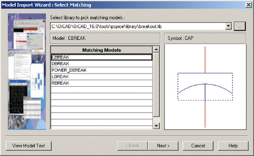
At the
Import Model Wizard dialog box (Figure 7-53), use the
Browse… button in the upper right-hand corner to find the PSpice model you want to associate with the Capture part. The wizard automatically searches through the PSpice library and lists all models in the
Matching Models window that have the same number of pins as the Capture part you selected in the Part Library Manager. Select the
CBREAK model and click
Next.
 |
| Figure 7-53 Matching parts with the
Model Import Wizard. |
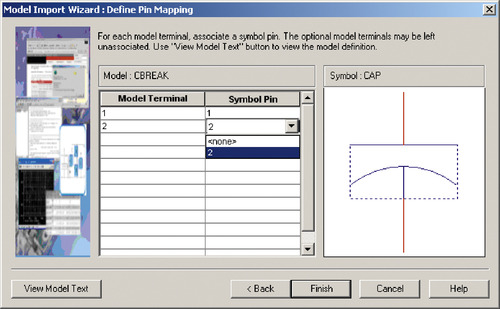
The wizard then displays the Pin Matching tool shown in Figure 7-54. This is where you connect the PSpice model pin to the Capture part pin. Click
Finish when the pins are matched. The information box shown in Figure 7-55 should be displayed, indicating that the capacitor now has a PSpice model attached to it.
 |
| Figure 7-54 Mapping pins with the
Model Import Wizard. |
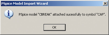 |
| Figure 7-55 PSpice model successfully added to a Capture part. |
Constructing Capture Symbols
Four types of symbols are used in Capture: (1) power/ground symbols, (2) off-page connectors, (3) hierarchical ports, and (4) title blocks.
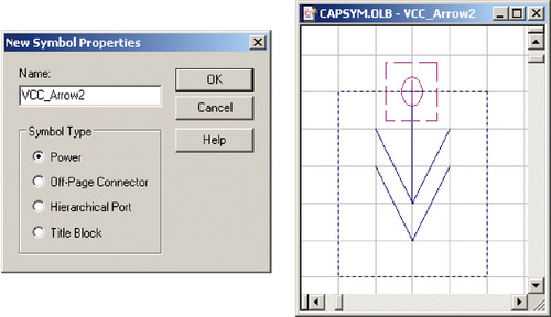
To make a new power symbol, open the
capsym.olb library. Select the
Library icon under the
Library folder. From the
Design menu, choose
New Symbol. In the
New Symbol Properties dialog box (Figure 7-56), enter the name and select the appropriate radio button from the
Symbol Type group box. Click
OK. A part editing window and drawing toolbar will be displayed. Use the graphics tools to make the symbol. Close the editing window and save the symbol. Save and close the library.
 |
| Figure 7-56 Making a new power symbol. |
The construction methods for power symbols, off-page connectors, and hierarchical ports are similar (although each has its own functionality). The title block is different from the other three. The two types of title blocks are default and optional. Every new project has a default title block, which you can specify for each project by going to
Options→Design Template… on the schematic page menu. You can also add optional title blocks by going to
Place→Title Block…, also on the schematic page menu. The title blocks are located in the
capsym library. You can construct your own title blocks and save them with the others or make your own library of power symbols, title blocks, and the like.
To make a new title block, open or make a new Capture library, select the
Library icon, and from the
Design menu, select
New Symbol…. At the
New Symbol Properties dialog box (Figure 7-56), select
Title Block and click
OK. Just as with the power symbols, you will be presented with a part editing window. Use the graphics tools to construct the box (Figure 7-57 shows an example of a parts list) and the Text tool to add titles and headers. To enter text that can be modified on schematic pages double click in a free area within the window to display the
User Properties dialog box. Click the
New… button to create new text objects. The name field is required but you can either leave the value field empty or enter a default value. Click
OK. To make an object field visible select
Part Properties from the
Options menu and click the
Display button in the
User Properties dialog box for the field of interest. After you have saved the block, you can add it to any schematic page.
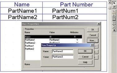 |
| Figure 7-57 Example of a new title block used as a parts list. |
That completes the chapter on making Capture parts and symbols.
..................Content has been hidden....................
You can't read the all page of ebook, please click here login for view all page.