
Chapter 5
Micromechanical Transducers
Chapter Contents
5.1 Application Fields
5.2 Overview of Materials
5.2.1 Single Crystals
5.2.2 Amorphous Materials
5.3 Thick and Thin Film Hybrid Materials
5.4 Microactuation
5.5 Packaged Sensors
5.5.1 From Die to Device Level
5.5.2 From Device Level to System
5.6 Silicon as a Mechanical Material in Resonant Microdevices
5.6.1 Resonant Sensors
5.6.2 Diaphragms as Micromechanical Couplers
5.7 Information Society
5.7.1 Micro-Opto-Electromechanical Systems
5.8 Conclusions
Miniaturized micromechanical-based transducers are applied in many various scientific communities and industries. In this chapter we look into the basic concepts of this extensive and important category of devices using simple components as examples. Transducers come in such extreme diversity that a descriptive overview such as is provided by this book is best taken from the perspective of the user. One of the most easily understood definitions of transducers is that they convert energy from one form into another. This perspective also shows that there is no one single design rule. The designer needs to start from a range of actual conditions to realize the required transduction principle in a given application.
At its heart a transducer is a component of a measurement system; the transducers at the input and the output of a measurement system are called sensors and actuators, respectively. We distinguish six different energy domains that need to be measured: radiant, mechanical, thermal, electrical, magnetic and chemical [1]. Transducers are present in both technical and biological systems. A great many transduction processes occur in natural (biological) systems, which are widely studied, mainly with respect to their importance in understanding disease and possible therapeutic interventions using pharmaceuticals. Researchers from all disciplines have investigated the functions appearing in natural systems for many decades, and recently more and more engineered systems have demonstrated that these natural functions can successfully inspire novel sensor and actuator designs.
Initial industrial developments focused on transduction in technically dominated environments, but there are many examples where technical and biological systems meet (medicine, biopharmaceutics, agriculture and the bioindustry). This chapter introduces the field of micromechanical sensors and actuators and their technical applications. In this context, the mechanical sensors and actuators that convert mechanical energy into electrical energy and vice versa are particularly interesting, since these devices are so essential to the design of many technical systems. Figure 5.1 presents a simplistic flow-chart of a system at a very abstract level.
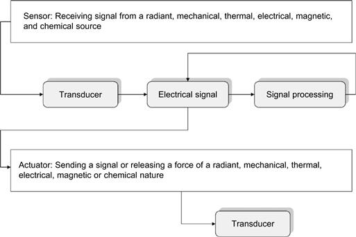
Figure 5.1 Very simplified technical interpretation of a system. This overview illustrates the central role of transducers.
The following sections will cover a variety of material and design aspects that are relevant to micro- and nanomechanical transducers. Any of the transducers which are introduced here as microactuators may be used in reversed operation as a sensor, and a vast amount of literature exists that describes micromechanical transducers in sensor applications. This field is too extensive to discuss details of engineering design and the theoretical background of sensors and actuators within the context of this book, hence we will focus on selected microfabrication technologies and their applications. The critical issues of packaging microfabricated sensors for real-world applications, however, are briefly mentioned.
I realize that the choice of topics covered here may appear to be randomly selected. To answer this, I would point out that the importance of this field lies not with any single new phenomenon, but the fact that our lives have been changed by developments from different disciplines and their integration into one system. This means that it does not much matter which examples are selected from the many currently being investigated. It is, however, important to mention the fairly novel combinations, such as optomechanical, electrochemical-mechanical, and (bio)chemomechanical devices, that have arisen in this field. A wealth of further reading is available on the details of microscale transducers and their backgrounds [2–5]. The examples presented here may be taken as an initial starting point for study in this field of research and development. Students may use the following sections as a guideline to the problems and design aspects of the various sensing and actuation principles, e.g., factors such as sensitivity, temperature dependency or material strength.
In the following section we will briefly introduce the field of applications, and after this we will discuss materials and methods in general and silicon resonant devices in particular. In this chapter, I will also discuss a hands-on case for the application of a resonant actuator based on my PhD project. This relatively simple example could be used in the practical part of a microfabrication course. The topic of modeling of such systems is beyond the scope of this book, and readers are referred to the examples published elsewhere [6].
5.1 Application Fields
When utilizing resonating elements as a sensor, a system parameter (e.g., mass, stiffness, strain) is changed. A shift of the eigenvalue of the system will then occur and this produces a readout for the measurand in the frequency domain. The miniaturization of such transducers is driven by a need for light weight, low cost of manufacture and ease of portability by hand-held formats. Ideally, these needs are fulfilled by the utilization of microsystems rather than precision engineering and fine-mechanical assembly. The latter may be possible but it is cumbersome and faces challenging structural limitations around lateral dimensions of 100 μm.
Although it is possible to build dedicated precision engineering assembly lines for structures in the micrometer range, many of the microfabricated sensors and actuator devices have actually been first demonstrated by utilizing the silicon micromachining technologies discussed in Chapters 2 and 3. These silicon sensor devices are more sensitive than their precision engineered counterparts. In the light of current economic demands, polymer electronics, and re-engineering of proven silicon microsystems into a polymer replication process can be considered as a possibility for large-scale production. A paradigm shift in materials selection has occurred because nanoscale sensors and actuators often rely on self-assembly at the scale of molecules and atoms, which enormously broadens the diversity of potentially applicable materials.
Design modeling is very important in the field of micromechanical sensors and actuators. A number of analytical models have been investigated and compared to numerical models of device designs. Understanding the governing formulae for theoretical and experimental modeling is a prerequisite for the optimization of such integrated systems. These sophisticated design studies for the fine-tuning of structural and energetic performance are important, because correction of the devices is often not possible once they reach the back-end of the process. Re-running a complete process would be extremely expensive. In many research projects, access to a microfabrication infrastructure often leads to the creation of demonstrators without any model-based design iterations. However, in commercial production environments modeling is extensively used to avoid design mistakes, and therefore costs.
As yet, only a few microelectromechanical devices or components have been successfully introduced into the real world. Reduction of design complexity and greater levels of accuracy need to be achieved first. The practical hands-on approach of research can help, because actually building the device and observing is still far easier than modeling it from scratch. It is important to realize that the modeling tools existing in industry are often based on the aforementioned observations and discoveries at the demonstrator level. While a reduction of complexity will improve production yields per batch, only better performance will make the devices competitive.
A type of micromachined sensor that is used in a multitude of industrial applications is the pressure sensor. Figure 5.2 (left) depicts the SMD085, which is one of the first micromechanical pressure sensors in a standardized SMD (surface mounted device) package, manufactured by Bosch. The sensor measures barometric altitude for an ambient pressure range of 0.6 to 1.15 bar. Figure 5.2 (right) depicts the new digital MEMS pressure sensor BMP085 of Bosch Sensortec, shown in its device package of 5 × 5 × 1.2 millimeters. The sensor is fabricated to conform with current developments and is intended to integrate navigation functions into mobile phones. The sensor has a resolution of up to 0.25 meters in altitude change and shows full conformity to the Restriction of Hazardous Substances (RoHS) directives, and is also halogen-free.
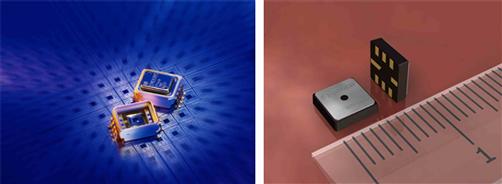
Figure 5.2 Packaged micromechanical pressure sensors manufactured by Bosch. Left: SMD085, and right: BMP085
Photos: Bosch, available online. [7].
The fabrication of such a system undergoes stringent process control conditions in Bosch’s production environment at Reutlingen, Germany. Figure 5.3 depicts such a process example.
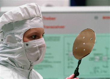
Figure 5.3 Wafer production at Bosch in their Reutlingen facility (Germany) under strict cleanroom conditions.
Photo: Bosch, available online. [7].
Sensor principles are currently under investigation for industrial applications. Fritz et al., for example, have investigated the translation of biomolecular recognition into nanomechanical signals. The research was conducted within a collaboration project between IBM Research and University of Basel, Switzerland, the results of which were published in the prestigious journal, Science [8]. They report the specific transduction, via surface stress changes, of DNA hybridization and receptor-ligand binding into a direct nanomechanical response of microfabricated cantilevers. These cantilevers were assembled in the form of an array, and were functionalized with a selection of biomolecules. The differential deflection of the cantilevers was measured as a consequence of molecular recognition during hybridization of complementary oligonucleotides. Other biomolecular interaction studies (protein A-immunoglobulin) have demonstrated the potential for the use of such nanomechanical transducers for the detection of biomolecular recognition. The surface modification method introduced by Shah and Abbott, who investigated the principle for measurement of chemical exposure based on recognition-driven anchoring transitions in liquid crystals, may allow even more smart ways to modify the novel sensor components than those introduced by Fritz et al. [9]. In 2007, Waggoner and Craighead provided a critical review of micro- and nanomechanical transducers for environmental, chemical and biological detection [10].
This work shows clearly that micromechanical pressure sensors made from silicon, by methods adopted from the integrated circuit industry, were just the beginning of this class of devices in the sensor market. We will now discuss application examples which show a potential for optically integrated functions for sensing applications. Micromechanical actuation as a source of excitation in resonant sensors and the principles of actuation in motors, relays, switches, valves and pumps will be covered, from the perspective of specific sensors and actuators in chemical engineering and biology.
5.2 Overview of Materials
5.2.1 Single Crystals
Single crystal silicon and silicon-based materials form the largest group of materials used for sensor designers since electronic-compatible production processes are available. Micromechanical sensor designs, however, tend to be much larger in the “footprint” silicon that they use than electronics components, with the smaller number of devices per wafer making production economically questionable. Other materials may be preferred if electronics are not to be integrated into the same platform, or when sensors are intended to operate in harsh environments or at elevated temperatures.
Single crystal quartz is an available, alternative substrate since it has been used routinely for timebase devices in electronics and watches. Gallium arsenide (GaAs) or sapphire (A2O3) substrates are used for special applications in the electro-optical domain. They are processed by wet chemical etching which is also used to manufacture diaphragms (often referred to as membranes), beams (called cantilevers in this field), and resonant masses (see Chapter 2 for an illustration of these basic structures in silicon and quartz). These speciality substrates are more difficult to work with than silicon, and to broaden the range of potential designs, dry etch processes have been developed.
These processes are readily available through a diversity of MEMS foundry services or cleanrooms, which are accessible through research centers and universities. So, one could say that a sensor designer is mainly restricted by cost versus performance issues rather than restricted access to an appropriate tool park.
Selection of the best materials and methods for a sensor design may be inherently linked to the background of the designer or the company commercializing the sensing device. The proper operating conditions for the device is the second factor in the choice of materials and methods for fabricating a specific transducer. For chemical sensors, for example, the advantages of integration into silicon are far less obvious, since the devices are often immersed in electrolytes that may short-circuit or shunt the electronics. Sensor packaging is therefore very important, and a substrate that is easier to package than silicon may be preferable. These conditions have driven the need for hybrid integration concepts in the biological and chemical domains, rather than in the mechanical or optical fields. We will return to some of these issues in the discussion of (bio)chemical sensors in Chapter 6.
5.2.2 Amorphous Materials
Micromechanical transducers often incorporate amorphous materials in the packaging of the device. Fused silica and glass are often used in silicon processing lines, and may offer certain benefits, particularly if low thermal conduction and dielectric constants are required in the design. Polymers are also used in this way, and can also actually comprise the sensing or actuator component. Use of these materials potentially reduces the production costs to the order of cents per piece if the device can be made in one injection molding cycle. Limited accuracy, poor machining and the large investments needed to install dedicated tooling equipment have limited the success of such amorphous materials in this area, although some recent investigations into SU-8 photoresist as a mechanical material may change this [11]. Ingrosso et al. have published the results of a functionalization procedure integrated with the fabrication of micromechanical SU-8 cantilevers in order to chemically bind organic-capped iron-oxide (Fe2O3) colloidal nanocrystals (NCs) at the photoresist surface, under visible light, ambient atmosphere and room temperature. Their concept resulted in a highly interconnected NC multilayer network, which was demonstrated to be appropriate for real-time detection of acetone vapor [12].
5.3 Thick and Thin Film Hybrid Materials
It is difficult to give a defined overview of materials that may be processed by methods as diverse as ceramic tape casting, screen printing, electroplating, lamination, laser machining and all the other techniques in precision engineering. Rapid prototyping print processes or fiber-(electro)spinning, for example, may form excellent materials for advanced micro-nanofunctional systems, but have not been considered due to lack of an identified need. The thin-film community has developed novel fabrication processes for materials that would not exist naturally, because of their hybrid nature or their assembly from fine-tuned layers (so-called multilayer systems). Any of these could be selected as materials in the design of a micromechanical transducer.
On the other hand, the automotive and compliance sensor technology market is highly cost driven, and requires the highest possible sensor performance at lowest manufacturing costs. Here, we can only conclude that with the rising manufacturing standards in the non-silicon industry and upcoming nanotechnology developments for creating novel materials, it is clearly not the integrated silicon industry alone that drives this market sector. We will address the selection of materials and fabrication techniques in the next section, in the context of the working principles of microactuation.
5.4 Microactuation
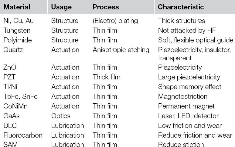
Table 5.1 presents an overview of structural materials, together with their use and principles of processing and the characteristic properties often explored for microactuation. Any material being considered for implementation into a transducer has its own design rules, as discussed in the literature.
Table 5.1 Overview of materials and application areas
One of the working principles often used at the microscale is electrostatic actuation, which, because of the small distance between the capacitor plates (realized by microfabrication approaches), is quite efficient. Oppositely to the efficient function of these small plate distance, it can lead to stiction effects during manufacturing processes and has to be specifically addressed in a process document by a suitable technique, e.g., freeze-drying [13]. Figure 5.4 depicts an example of this electrostatic working mechanism in the actuation of a cantilever, as discussed in Batra et al. [6].
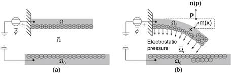
Figure 5.4 Illustration of electromechanical coupling in electrostatic MEMS. (A) Device prior to applying electrostatic pressure and (B) devices during applying electrostatic pressure.
Reproduced from [6] with permission from IOP Publishing Ltd.
Some materials directly convert the initial source of energy, for example thermal (shape memory alloys) or electrical (piezoelectric) energy, into mechanical movement. Piezoelectricity should be highlighted in MEMS technology. It occurs naturally in certain crystal structures, such as single crystal quartz, but the effect can be created more efficiently in artificial materials, e.g., which exploited the perovskite structure of lead zirconate titanate (PZT). This special material has been used many times in industrial applications. The environmental concerns regarding the use of lead-containing components require alternative piezoelectric materials to be sought. Another reason for the search for lead-free piezoelectric materials are their application at high temperatures.
One other typical microactuation mechanism uses temperature changes to drive mechanical displacement. This can be done with a bimorph (e.g., bimetallic) strip, which uses the mechanical forces caused by the difference in thermal expansion coefficient of the two materials in a thin strip. This difference causes the strip to bend, and can be incorporated into a cantilever design.
Pneumatic expansion and contraction, shape memory or material phase-change caused by the heating or cooling of the system may also be used to create a thermo-reactive transducer, other means of actuation may be magnetic force transduction. An introduction to the design, manufacture and nanoscale engineering of these mechanisms appropriate to an academic undergraduate course is presented in MEMS and Microsystems by Tai-Ran Hsu [14].
5.5 Packaged Sensors
Piezoresistive, capacitive and in some cases optical read-out miniaturized pressure sensors make use of a micromachined diaphragm. The capacitor is a simple sensor, made of two parallel plate electrodes. One of the electrodes is also a diaphragm. Diaphragms can be fabricated by silicon etching methods, as discussed in Chapter 2. They are very stiff, and allow controlled displacement of the diaphragm electrode against its counter electrode when a pressure is applied. They are typically a square of 1 × 1 mm2 with a thickness of 20 μm. The opposite static electrode is often made directly from the encapsulation material, which is made conductive by a thin film.
The parallel plate structure finds application for pressure sensors, accelerometers and interferometers. Because the capacitances of such sensors are small, stray capacities should be avoided, and the electronic circuitry should preferably be located close to the sensing element. Glass-to-silicon anodic bonding is often utilized as a packaging technique for encapsulation of silicon-electronics. Using the substrate itself as packaging allows encapsulation at the wafer level, thus reducing the costs of batch fabrication and small chip size [15–17]. For the examples depicted in Figure 5.2 in Section 5.1, manufacturers have to consider the assembly at chip (often called die) level, device level (packaging into a housing) and the packaging of microsensors at system level. The latter will have to withstand performance testing based on the end-user requirements. A variety of technical solutions were developed for die-level assembly that are considered as CMOS compatible at the back-end of the processing of a sensor. Some processes may still be conducted at the level of the wafer (batch processing), or allow at least easy mounting of the packaged die onto a printed circuit board (PCB). The PCB contains the drive and read-out electronics of the system.
Eventually the individual sensors at the die-level have to be encapsulated by a packaging technique, to protect the delicate mechanical microstructure from the environment. The following subsections summarize key aspects of the packaging process.
5.5.1 From Die to Device Level
A piezoresistive, micromachined, silicon pressure sensor die is often manufactured by a step-and-repeat lithography across the wafer surface. The silicon is etched to create the diaphragm at the wafer level, and the result is bonded to a glass wafer. The individual dies must then be separated into single dies (called dicing), utilizing a circular, diamond, sawing plate. Wafer dicing is carried out on a specially prepared dicing frame (called a chuck) that allows high precision movement of the table from dicing line to dicing line and controlled depth of dicing.
The individual dies are then mounted by pick and place procedures onto the support plate (called a header) that contains the electrical feed-through interconnects and a mounting rim for the casing. Both header and casing are made either from metal or plastic. In some applications, the casing is required to be highly corrosion-resistant or stable at very high temperatures, which demands different packaging solutions.
Plastic encapsulation is commonly used in integrated electronic circuit manufacturing, but no standard packaging procedure applies to all microdevices, and each supply company may have their own favored packaging line. The customer then may reassemble the packaged sensor into a new package, although it may have been better to construct the initial sensor package according to the customer’s needs. From the point of view of the mass manufacturing of sensors for different markets, however, the latter is economically more attractive for the supplier.
Figure 5.5 illustrates a cross-sectional view of a die-level package with the electrical interconnects leading to a PCB. Mounting the pins onto an external electronics PCB board, and housing this combination of the electronic board and the packaged die produces a device-level package. At this stage the pressure sensor can be operated as a standalone device, but it is often part of a system controlling an industrial process etc., and therefore needs to be further assembled into a device-level package.
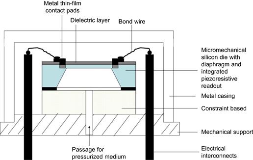
Figure 5.5 Assembly of a die into a package.
Figure is drawn based on examples presented by Hsu [14].
5.5.2 From Device Level to System
One example for a fully packaged system is the VPFlowScope made by VP Instruments BV, Delft, The Netherlands. The VPFlowScope combines mass flow, pressure and temperature sensors into one measurement system, combined with a built-in data logger. The system-level package is compatible with a special installation procedure, called hot tap drilling, which allows installation points to be created in compressed air piping without interrupting the compressed air supply. This system level package makes the VPFlow- Scope easy to install and to use as an all-in-one instrument for compressed air measurement and similar applications.
Compressed air systems are installed to support many different types of industrial production processes. The users of such systems often rely on the proper function of the compressed air pipes, however, leakage, misuse or other reasons for non-optimal configurations in the piping system may lead to additional costs. Using a flow-management system may give cost savings of up to 50% of the current operation. Although the pressure sensor integrated with the VPFlowScope is not based on a capacitive diaphragm, as discussed above, it utilizes silicon micromachining in its pressure and flow sensing elements with smartly integrated electronic temperature compensation and is therefore a good example of the micro system-in-a-package approach. Figure 5.6 shows the system components as a starting installation kit (left), a typical installation environment of a compressed air system ( middle) and a close-up of a VPFlowScope installed into a pipe line (right). More information may be obtained from the company’s website [18]. The measurement principles and design considerations of the type of devices adopted in the product range of VPInstruments have been presented by van Putten et al. [19].
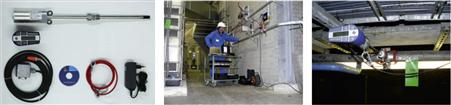
Figure 5.6 Example of an assembly of different sensor devices into one user-proof system package ready to use by the customer: VPFlowScope installation starting kit (left), a typical operating environment (middle) and the installed VPFlowScope (right).
Image courtesy: VPInstruments BV. Figures available online. [18].
5.6 Silicon as a Mechanical Material in Resonant Microdevices
Silicon and the associated integrated circuit fabrication techniques have been the most investigated material and fabrication methodologies for mechanical sensors for the last three decades. This can be largely explained by the success of silicon in the batch fabrication of electronic devices. There is as yet no reasonable replacement as a handling wafer if one considers that some electronics may be integrated into an innovative sensor. Industrial interest mainly centers on redundancy and organizing multiple sensors in one platform. The benefits of using silicon have clearly sustained research and development by various successful transitions to industry for applications employing temperature sensors, pressure sensors and accelerometers. One special class of sensors works at resonance, whereas the principle of measurement relies on a frequency-shift, providing an output signal very attractive for precision measurements as well as new implementation areas, such as for example measuring molecular interactions [8, 20]. The introductory section of the publication by Tilmans et al. summarizes some key aspects and developments concerning resonant devices, so the next subsection uses their wording [21]. Tilmans, who works at the respected IMEC Institute, Leuven, Belgium, is an expert in this field, and has successfully translated these types of devices to industry for many years. Other overviews of this field of research are the paper on “Resonant silicon sensors” by Stemme published in 1991 [22], the comprehensive Handbook of Sensors and Actuators, in Volume 8 of which (edited by Middelhoek), Bao discusses micro mechanical transducers [4, 23]. Elwenspoek and Wiegerink have presented a book specifically on Mechanical Microsensors, which covers the essential development stages, design and applications of resonant microdevices [3].
5.6.1 Resonant Sensors
Resonant sensors provide, in addition to their excellent stability, resolution and accuracy, a signal output in frequency form that is immune to intensity fluctuations, and allows the devices to be easily connected with digital systems, which is required for its effective employment as a measurement device. The structure should only respond to changes in the load to be measured. We have already briefly discussed the pressure sensor in Section 5.5.1. One of the first resonant strain gauge-type pressure transducers was described by Belyaev et al. in 1965 [24]. In their design, the strain gauge is mounted on top of a diaphragm by means of two brackets. Similar designs were also introduced by Greenwood [25] and Thornton et al. [26]. Silicon bulk micromachining was used to fabricate these devices. Ikeda et al. presented a pressure sensor design in which the resonators are held in evacuated microcavities on top of the diaphragm. Operating in a vacuum enhanced performance tremendously, gaining a so-called higher Q-factor (Q = quality) [27]. This group used the single-crystal silicon, considered to be a classical construction material, in combination with selective epitaxial growth techniques and a high boron etch stop for the fabrication of the device by etching in ethylendiamin perizine (EDP). The latter is no longer used in production environments. An alternative way of fabricating a sealed resonator device was reported by Guckel et al. [28], who used the deposition of a fine-grained polysilicon layer by LPCVD and sacrificial layer etching to construct their device. Both technologies are very attractive because of their ability to manufacture in batches. We will discuss some of these aspects in more detail in the following section, but focus here on silicon as a mechanical material. Because most device designs for sensor systems are inherently difficult to comprehend, we will first give a design example for the application of silicon as a mechanical material, by describing the case of a three-sides clamped diaphragm.
5.6.2 Diaphragms as Micromechanical Couplers
Although the structure discussed here was originally designed as an actuator for a micro-optical scanning device, it may also be utilized in the design of a resonant cantilever-type sensor. Diaphragms are clearly one of the basic building blocks in micromechanical sensor and actuator design, and their different resonant behavior with respect to clamping is an interesting field of research.
Figure 5.7 depicts a diaphragm with an integrated boss-feature (also called a mesa). This mesa allows the micromechanical cantilever to be connected to the microactuator at a later processing stage. The diaphragm has been etched in a KOH bath at the wafer-level, and at the back of the wafer a thin film of gold has been deposited to create a conductive layer. Subsequently the wafer has been diced and the diaphragms mounted on a frame, which is shown in Figure 5.8. To excite the micromachined structure, a commercial piezoelectric PZT-disc has been glued to the back of the diaphragm using silver-epoxy, which connects the piezo-disc electrically to the gold layer and to the frame, respectively. The opposite side of the piezo-disc is wire-bonded to an isolated printed circuit board (PCB) that was also mounted to the frame using epoxy glue. Standard electrical cables can then be used for the connections from the frame and the PCB to the frequency generator providing a sinusoidal output voltage to the piezo-disc for excitation.
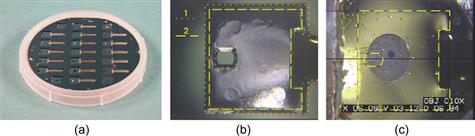
Figure 5.7 Silicon diaphragm fabricated by silicon micromachining. A commercial piezo-element is mounted to the diaphragm applying a mechanical excitation source by a small sinusoidal drive voltage to the piezo, which will subsequently drive the membrane into resonance at its eigenvalues. View at wafer-level (a), diaphragm top-view with mesa at the left-hand side of the diaphragm (b) and mounted piezo-disc at the back of the diaphragm, dashed lines mark the diaphragm area (c).
Reproduced from R. Luttge, PhD Thesis, 2003, University of London, UK.
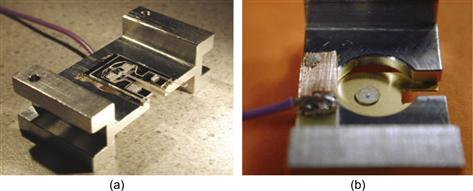
Figure 5.8 Mounted diaphragm on aluminum support frame including a view with a hybrid-integrated glass cantilever component bonded to the mesa-structure of the diaphragm, whereas the components act together as barcode reading scan head device, (a) and a view onto the connected piezo-disc at the back of the diaphragm with PCB and cable connector (b).
Reproduced from R. Luttge, PhD Thesis, 2003, University of London, UK.
Figure 5.8 shows the completed microelectro(opto)mechancial system, which includes a glass cantilever for the integration of an optical function into the system (not further discussed here), all mounted on a conventionally milled aluminum frame for testing the device on an optical bench. In this specific design, the wafer-level manufactured diaphragm is intended to provide micromechanical coupling between a commercially available non-CMOS compatible PZT element and another non-CMOS compatible optical integrated cantilever device. The micromachined silicon diaphragm can also function as a platform for full electronic integration of a micro-opto-electromechanical system (MOEMS) (for more details on MOEMS, see Section 5.7.1 below, and also Chapter 3, Section 3.5.2).
Figure 5.9 shows the first five eigenvalues of a three-sides clamped diaphragm, assuming an idealized design without the coupled mass of the mesa, the piezo-disc or the cantilever. Knowledge of the resonant frequency is a key parameter in the design optimization of a resonant system. Of course the damping of the system also plays an important role. Excessive damping would prohibit resonance, and too little might damage the system. For micromechanical cantilevers, large quality factors have been achieved (1000 or higher), therefore the damping ζ can have very small values while critical damping occurs at ζ = 0.2.
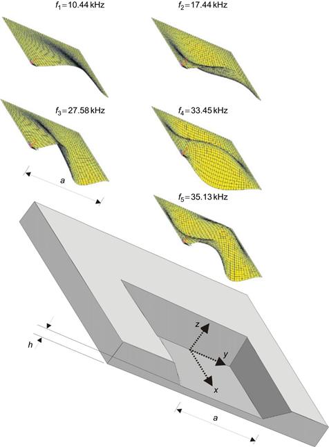
Figure 5.9 Visualizing the eigenvalues or mode shapes of a diaphragm clamped at three sides. Mode shape surface plots generated numerically by E. Oosterbroek for a rectangular silicon diaphragm with side length a = 6.5 mm and a diaphragm thickness h = 45 μm.
Reproduced from R. Luttge, PhD Thesis, 2003, University of London, UK.
5.7 Information Society
Microtechnology not only offers a reduction in device size, but also enables cost-efficient fabrication via the parallel output of many components – so-called batch processing. Once it has been determined that a miniaturized system would enhance performance, and be economically viable in large-volume production, this parallel processing approach will then repay the initial (large) investment. The overview of studies in this chapter are an introduction to the paradigm shift of industrial applications caused by the evolution of microfabrication technology. All engineering disciplines have benefitted from previous developments in integrated circuits processing techniques, and this has fed into applications by inter- and multidisciplinary research, which have yielded novel fields of systems design such as MOEMS, BioMEMS and microreactors.
All these different fields have specific materials, requirements and robustness, sensor selectivity and sensitivity, as well as accuracy and precision specifications. Sensors in the field of BioMEMS and microreaction technology will be discussed in more detail in Chapters 6 and 7, and the following subsections cover a variety of cases which are either fully commercialized or investigated thoroughly at component level from a market perspective. Information technology (IT) is still the most advanced commercial user of sensor applications. However, all other sectors are benefitting from the early-adopter position of IT, and follow the trend of the More-than-Moore concept, which further promotes the systems-on-a-chip approach for micro-nanomechanical sensor systems.
5.7.1 Micro-Opto-Electromechanical Systems
Optical engineering consists of the fabrication and assembly of optical components, such as lenses, mirrors, prisms, and refraction and diffraction elements. One could include the mechanical features of waveguiding applications such as light distribution, signal modulation and retrieval in this category. It is possible to emulate some of these optical components at the micro domain, but the features that move along a two-fold axis (micromirror) and the passive alignment of components remain as critical design problems. Fiber couplers and out-of-plane mirror elements are examples of devices which face these limitations. Although at the end of the 1990s there was a major economic dip in the telecommunication market because of the dot com meltdown, still MOEMS industrial developments and cutting-edge system design research has progressed. Some of the first successful industrial products spinning off the continuous developments in MOEMS were portable point-of-sales barcode readers (Figure 5.10), text-recognition and advanced e-reading headset systems (Figure 5.11), and micro-mirror integrated digital projectors and displays (Figure 5.12).
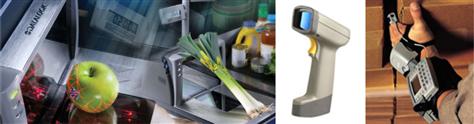
Figure 5.10 Datalogic Magellan 8500XT retail barcode scanner (left, source: Datalogic, reproduced from image accessed via online distributor site, 2011), hand-held scanner (middle, source: Symbol Technologies, reproduced from image accessed via online distributor site, 2003) and integrated wearable WT4000 (Motorola) scanner series on finger, which allows use of both hands for other actions (right, source: Symbol Technologies, reproduced from image accessed via online distributor site, 2003.)

Figure 5.11 Diversity of scanning tools. Head-mounted retina display (left), hand-held text scanner (middle) and scanner for recognition of barcodes (right).
Reproduced from images accessed via online distributor sites 2003.
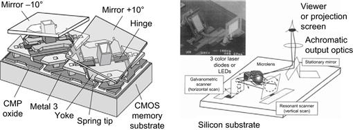
Figure 5.12 MEMS-based digital mirror projection display (left, reproduced from [32] with permission © IEEE 1998) and another type of display device configuration (right, reproduced from reference [33].)
Barcode readers are used for in-store inventory, document management, vehicle registration, etc. So they need to be lightweight and portable. Examples of such systems are presented in Figure 5.10. The technology for barcode reading has applications in a variety of industries, such as healthcare, mobile data collection and manufacturing. Portable systems may be based on different technologies including contact scanning, CCD imaging and laser scanning, of which the systems depicted in Figure 5.11 give some examples. In general, laser scanning is achieved by beam deflection using a galvo-mirror, with the returned light being collected and focused onto a photodiode by a parabolic mirror.
New systems in micro-optics rely on surface micromachining, deposition and patterning of polysilicon in a sequence with sacrificial layers to obtain movable structures. We discussed the principle of surface micromachining in Chapter 2, Section 2.3.2. Examples of these micromachined optical-integrated systems are illustrated in Figure 5.12. One approach in micro-optics is to redirect light by actuated mechanical carriers known from switching devices [29, 30], but this does not incorporate an integrated waveguide. Also, the advanced waveguide switching devices that do exist lack adequate displacement range. An alternative approach miniaturizes the conventional optical bench, which leads to a large number of very impressive scanning display devices using resonant mirror components and comb drives to actuate them. Tien et al. have published examples of such micro-optical benches for scanning devices. These are depicted on the right-hand side of Figure 5.12. This type of device requires an increased number of total components, which may be not acceptable for certain production lines. Over the years, surface micromachining technology has matured commercially. The service is offered by MEMSCAP, Inc., a successful French MEMS service supplier. The cost for a multi-user MEMS process (MUMPs) using either the polysilicon, metal or SOI process line with a standard die site on the wafer of 1 cm × 1 cm and a total of 15 unreleased die delivered to the client is 3700 US-dollars/run for academic use and 5300 US-dollars for non-academic use. [31]
Power splitters, and more advanced systems such as waveguides, optical amplifiers and modulators, have been fabricated for telecommunication devices and photonics. Wu et al. present an overview of optical MEMS technology [34]. A marriage between previously developed processes for microelectromechanical systems and optical systems has led to the emergence of the research field of micro-opto-electromechanical systems (MOEMS).
When I conducted my PhD research at the Optical and Semiconductor Devices Group, Imperial College, London, UK, I was part of the research team of the Optical Scanner Project headed by Prof. Syms from the years 1999 to 2003. In this context, I wish to acknowledge funding by the EPSRC (British Research Council). In the realm of the many market opportunities associated with integrated optics in the late 1990s, I investigated fabrication technologies for optical scanners based on micromachined cantilevers. This Resonant Cantilever Optical Scanner (RCOS) is an example of the application of MOEMS technology.
One of the objectives in the design of a barcode reading scan head device (depicted in Section 5.6.2, Figure 5.8) is to allow the integration of electronic components in the system prior to the back-end MST processing of the diaphragms. For aluminum integration, for example, the thermal budget must be lower than 450°C. The MST processing steps have therefore to be chosen appropriately to avoid destroying the electronics previously realized in the chip. Besides this obvious need for strict temperature control, micromachining in SC-quartz, for example, should also stay below 500°C because otherwise a transition from piezoelectric α-quartz to non-piezo β-quartz occurs, which would jeopardize the prospective of a high integration density. Multiple functions within same material (monolithic integration) would be no longer attainable. This section will therefore quote some examples from the literature which are relevant to the investigation of process technology for optical films at a modest temperature range.
We have already discussed various optical film deposition techniques and their impact on PLCs in Chapter 3. The examples of sol-gel based PLC, epitaxial deposition and sputtered optical layers complete this overview. High quality and relatively low manufacturing costs of spin-on glasses makes them attractive for the mass fabrication of devices. Passive sol-gel based integrated devices have already been demonstrated in earlier research, for example, at the Optical and Semiconductor Devices Group [35–38].
Cheng et al. [39] described a spin-on-glass process that simplifies the usually much more complex PVD or CVD deposition of lithium tantalate (LiTaO3) layers. This enables many applications that use piezoelectric, non-linear optical, electro-optical and acousto-optical properties within MOEMS. Lithium tantalate is spin-coated under a nitrogen atmosphere from a solution of LiOC2H5 in ethanol with Ta(OC2H5) onto silica-on-silicon wafers. The paper gives a detailed characterization of multilayer thick films resulting in a root-mean-square surface roughness of Ra = 6.3 nm and a refractive index of n =1.84 measured at the 633 nm wavelength. However, elevated temperatures of 600 °C were needed [39].
Plasma enhanced CVD is an attractive alternative technique for deposition at a lower temperature range, which can be used to create MOEMS fiber-to-waveguide couplers. Typically, deposition takes place between 200°C and 350°C. Figure 5.13 shows a device that is based on silicon-oxy-nitride (SiON)-on-silicon technology [40]. To obtain a high coupling efficiency it is important that the optical mode profile of fiber and planar guide are matched [41]. This can be achieved either by a lens, prism, grating or a tapered end of the waveguide. When using a tapered end, as suggested by de Ridder et al., fabrication techniques must be used that have tight control of tolerances, to achieve a very sharp point (taper radius smaller than 500 nm) for optimal optical performance [40]. The proposed design, shown in Figure 5.13, can be realized with only moderate demands on the quality of the photolithographic pattern definition. A so-called spot-size transformer for fiber-to-chip coupling is presented. This example of SiON deposition with a refractive index of n = 1.7 and a thickness of 300 nm for single mode propagation can be also utilized in RCOS design, which has been briefly mentioned above.
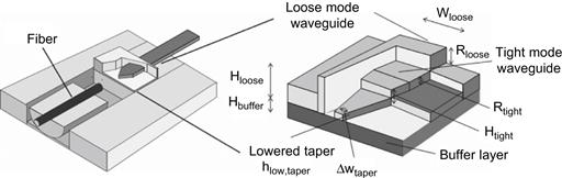
Figure 5.13 Optical integrated device for fiber-chip coupling using SiON/SiO2 waveguide technology.
Figure redrawn from reference [40].
Another possible coating technique for a silicon MEMS-based integrated optical device is thin film magnetron sputtering of Al2O3. During magnetron sputtering, slab waveguides can be deposited from an Al2O3 target in an argon gas atmosphere containing some oxygen. A photoresist mask can be applied to the layer and subsequently the Al2O3 slabs can be patterned by accelerated argon ion milling [42]. This approach results in low roughness along bends. For telecommunication applications the quality of the material must be enhanced by an annealing step at approximately 700°C or higher. However, the magnetron sputter technique could be considered without the additional temperature treatment for less demanding applications, similar to the above mentioned RCOS for barcode reading. M.K. Smit developed this process during his PhD project at the Delft University of Technology, The Netherlands. His thesis also details many other materials and fabrication aspects involved in the design of integrated optical applications. He describes functional optical designs and gives a comprehensive overview of the theoretical background of waveguides, including computation for bends, couplers and optical phased arrays. Essential parameters and measurement methods for the characterization of waveguides are also given [42]. A variety of text-books and review papers provide a good starting point for advanced reading on MOEMS and integrated planar optics [34, 43–45].
PECVD is a potential alternative to the magnetron sputter technique for making low-temperature optical slab waveguides. Kim et al. [46] have investigated the microstructure of this type of film. Figure 5.14 depicts a cross-section of an AlOx film on silicon. Low-loss alumina waveguide fabrication by atomic layer deposition (ALD) suitable for the ultra-violet and visible spectral regions has been recently reported by Aslan et al. [47]. ALD films were deposited at 200°C and 300°C, and are potentially useful for several integrated optical devices, which may include post-CMOS integrated applications.
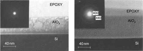
Figure 5.14 Cross-sectional TEM micrographs and diffraction patterns of aluminum oxide films deposited at 120°C (left) and 250°C (right).
Reproduced from reference [46].
Until the early 1990s, optical integrated circuits (OICs) concentrated on monolithic techniques to confine light into a guiding region for mixing or splitting, with integrated laser technology being used to make compact laser diodes, or to develop other opto-electronic devices in a variety of semiconductor materials. Typical techniques for the fabrication of waveguides are derived from thin-film processes, such as physical and chemical vapor deposition and subsequent patterning by photolithographic means. The use of thick oxide layers (2–20 μm) as an optical buffer layer on silicon wafers is one of the most widely used techniques for telecommunication applications, where the wavelength is in the micrometer range. The optical buffer layers are applied to the silicon by flame hydrolysis, which results in highly stressed silica. This is not suitable to be released from the silicon substrate, hence both the silica and the substrate are lost to further micromechanical usage in MOEMS. Nevertheless, thick buffers are needed to minimize the absorbance of light into the silicon substrate. The techniques addressed above may already present a solution to monolithic integration of the RCOS. However, when silicon micromachined cantilevers are employed in the RCOS design, thick claddings would be unavoidable, which suggest that the waveguide-cladding-cantilever microstructure could not be released from the substrate. Since a free-moving cantilever with integrated optical function is the aim of the project, other means of integration technology must be found.
To overcome such problems is standard industrial practice, hybrid solutions for optical device integration are frequently sought. If the two process lines for electronic and micro-opto-mechanical techniques are strictly separated, production of an integrated RCOS becomes much more feasible by using already established foundry services for the realization of the required functions. Only the final packaging steps of combining the opto-electromechanical integrated devices by means of subsequent processing of the MEMS/MOEMS structure onto the electronic component wafer would require a low thermal budget.
With respect to RCOS, Roberts et al. have presented some results based on precision engineered scan units [48, 49]. A light-guiding optical fiber served as a cantilever and was mounted on a commercial piezoelement actuator. Work performed by Roberts et al. led to the conclusion that fine-mechanical assembly of components, even on a cm-scale, is not sufficiently reproducible for a production process. A reduction of device size, and eventually spot size, is expected to enhance scanner performance, which allows for new applications to be developed. The demands for optical scanning in the fields of medical endoscopy, display accessories embedded in lightweight head mounts or even cosmetic spectacles, are a driving force for the continuous reduction of device dimensions. The realization of precisely directed illumination from a single mode integrated waveguide in a variety of wavelengths could lead to many other devices, for example, in metrology, ophthalmology or other medical applications [50–52].
5.8 Conclusions
The main aim of this chapter is to address the challenge of integrating skills and technologies from different scientific disciplines onto one chip. The demand of pure monolithic integration in one and the same material (mainly silicon) places limitations on the system. The engineer always has to compromise between the material properties and its fabrication capabilities. Development efforts should be focused on new applications, which combine optimized microtechnological feasibility with the best choice of material. For example, a variety of non-linear optical effects can only be produced with certain opto-active materials. To manufacture new products, new technological combinations should be explored, geared towards high efficiency. Although silicon is an excellent MEMS material, researchers have meanwhile also developed batch fabrication processes for other materials (see, for example, the processes described in Chapter 3). Section 5.2 has given an overview of different materials which are used in micromechanical sensors and actuator designs. However, continuous development in defining and shaping novel materials is required in order to meet the demands of a new generation of application fields. These different materials also require different mounting techniques, for example, index matching adhesives and other bond mechanisms were developed to meet technical and optical requirements [53].
Development strategies within the information technology industry are mainly based on functions in the electrical, magnetic or optical domain, and their combinations. Most techniques, from top-down approaches to the manufacture of sub-micron features described in Chapter 2, are generally applicable for integration in all the different energy domains. However, as we discussed in this chapter, the optimum choice of materials and process depends on the function of a specific system or component, the existing production capabilities and the product-to-market combination.
Microelectronic devices already regulate, control, enhance and dominate daily life. Think of your overfull e-mail or voice mail box in this context. Furthermore, the effectiveness of a modern city depends entirely on computerized technology for transport, finance and other customer services (e.g., banks, insurances, health care services). Think about all the plastic cards in your purse that give you access to these digital networks. The application of microsystems technology helps to save resources and to enhance operational performance. As in other fields, optical instrumentation went through a process of miniaturization, too, utilizing micromechanical transducers. Many new application fields are being explored at the investigator level, e.g., in the context of nanomechanical transducers for the identification of biological recognition processes, and are all intended to improve human life and the environment. If one does not yet know the specific answers that address an immediate problem, gathering information (sensing) is the first step towards innovation in any inquiry.
Specifically with respect to technological advances in the context of microfabrication for industry, microsystems technology (MST) has found that certain prohibiting effects on a macroscale can become useful for engineering at the micro level, e.g., the effect of resonance discussed above. MST combines the fabrication of components to exploit effects on the microscale with all other factors of systems design known from the conventional engineering approach. Furthermore, the process of miniaturization leads to new discoveries, such as the use of photonic crystals to manipulate light [54, 55].
When optical strategies were combined with microelectronics, the optical integrated circuit (OIC) was developed, based on optical waveguides instead of electrical conductors (see also Chapter 3, Section 3.6) [56, 57]. OICs are based on similar fabrication techniques to microprocessors, as they have been used for the manufacture of microprocessors. Their production uses thin-film integration concepts and in-plane operations, hence an optical integrated device is also often called a planar light circuit (PLC). In early efforts, which relied on planar techniques, mostly monolithic (i.e., all components fabricated on/in the same substrate) integrated approaches were pursued. However, the field of research and applications has grown so fast that existing technologies have not always been capable of delivering fully monolithic integrated devices with the desired level of performance. Also, niche markets need to use hybrid devices to speed up the development cycle and lower the cost of technical solutions by using standardized pre-packaged components. Powering a new generation of optical networking will require process and device synthesis on a much higher level of systems integration than is currently possible. The reliable demonstration of the merging of micromechanical and optical systems is a model case for further innovation by integration of micromechanical sensors and actuators with higher level architecture systems.
REFERENCES
1. van Putten AFP. Electronic Measurement Systems Englewood Cliff, NJ: Prentice Hall; 1988.
2. Wilson J. Sensor Technology Handbook Oxford: Elsevier, Newnes; 2004.
3. Elwenspoek M, Wiegerink R. Mechanical Microsensors (Microtechnology and MEMS) Berlin: Springer; 2001.
4. Bao M-H. In: Middelhoek S, ed. Oxford: Elsevier; 2000; Micro Mechanical Transducers: Pressure Sensors, Accelerometers and Gyroscopes Handbook of Sensors and Actuators. vol. 8.
5. Eaton WP, Smith JH. Micromachined pressure sensors: review and recent developments. Smart Mater Struct. 1997;6:530–539.
6. Batra RC, Porfiri M, Spinello D. Review of modeling electrostatically actuated micro- electromechanical systems. Smart Mater Struct. 2007;16(6):R23–R31.
7. http://www.bosch-press.de (accessed 07.04.11).
8. Fritz J, Baller MK, Lang HP, et al. Translating biomolecular recognition into nanomechanics. Science. 2000;288:316–318.
9. Shah RR, Abbott NL. Principles for measurement of chemical exposure based on recognition-driven anchoring transitions in liquid crystals. Science. 2001;293:1296–1299.
10. Waggoner PS, Craighead HG. Micro- and nanomechanical sensors for environmental, chemical, and biological detection. Lab Chip. 2007;7:1238–1255.
11. Calleja M, Nordström M, Álvarez M, Tamayo J, Lechuga LM, Boisen A. Highly sensitive polymer-based cantilever-sensors for DNA detection. Ultramicroscopy. 2005;105:215–222.
12. Ingrosso C, Sardella E, Keller S, et al. Surface functionalization of epoxy-resist-based microcantilevers with iron oxide nanocrystals. Adv Mater. 2010;22(30):3288–3292.
13. Deladi S, Svetovoy V, Krijnen GJM, Elwenspoek MC. Flash release – an alternative for releasing complex MEMS devices. J Micromech Microeng. 2004;14(12):1659–1664.
14. Hsu T-R. MEMS and Microsystems Hoboken, NJ: Wiley; 2008.
15. Esashi M. Encapsulated micro mechanical sensors. Microsyst Technol. 1994;1(1):2–9.
16. Esashi M. Wafer level packaging of MEMS. In: TRANSDUCERS 2009 – 15th International Conference on Solid-State Sensors, Actuators and Microsystems. 2009;9–16.
17. Esashi M. Micro/nano electro mechanical systems for practical applications. J Phys: Conf Ser. 2009;187(art. no. 012001):1–10.
18. VP Instruments. www.vpinstruments.com, (accessed 07.04.11).
19. Van Putten AFP, Van Putten MJAM, Van Putten MHPM. Silicon thermal anemometry: Developments and applications. Meas Sci Technol. 1996;7(10):1360–1377.
20. Langdon RM. Resonator sensors – a review. J Phys E: Sci Instrum. 1985;18(2):103–115.
21. Tilmans HAC, Bouwstra S, Fluitman JHJ, Spence SL. Design considerations for micromechanical sensors using encapsulated built-in resonant strain gauges. Sens Actuators: A Phys. 1990;25(1–3):79–86.
22. Stemme G. Resonant silicon sensors. J Micromech Microeng. 1991;1:113–125.
23. Handbook of Sensors and Actuators. Regtien P, ed. Oxford: Elsevier; 2004; Measurement Science for Engineers.
24. Belyaev MF, Dorzhiev DD, Etkin LG. Vibration-frequency pressure transducer. Instrum Constr. 1965;10:10–13.
25. Greenwood JC. Etched silicon vibrating sensor. J Phys E: Sci Instrum. 1984;17(8):650–652.
26. Thornton KEB, Uttamchandani D, Culshaw B. Novel optically excited resonant pressure sensor. Electron Lett. 1988;24(10):573–574.
27. Ikeda K, Kuwayama H, Kobayashi T, et al. Silicon pressure sensor integrates resonant strain gauge on diaphragm. Sens Actuators: A Phys. 1990;21(1–3):146–150.
28. Guckel H, Sniegowski JJ, Christenson TR, Raissi F. The application of fine-grained, tensile polysilicon to mechanically resonant transducers. Sens Actuators: A Phys. 1990;21(1–3):346–351.
29. Hoffmann M, Kopka P, Voges E. Optical fibre switches based on full wafer silicon micromachining. J Micromech Microeng. 1999;9:151–155.
30. Conant R, Nee J, Lau K, Muller R. Dynamic deformation of scanning mirrors. In: EEE/LEOS Conference on Optical MEMS. 2000;49–50.
31. Memscap Mumps pricing. http://www.memscapinc.com/nc-pmumps.pricing.html, 2011 (accessed 07.04.11).
32. Van Kessel PF, Hornbeck LJ, Meier RE, Douglass MR. A MEMS-based projection display. Proc IEEE. 1998;86(8):1687–1704.
33. Tien NC, Solgaard O, Kiang MH, Daneman M, Lau KY, Muller RS. Surface-micromachined mirrors for laser-beam positioning. Sens Actuators A. 1996;52(1–3):76–80.
34. Wu X-F, Dzenis YA. Guided self-assembly of diblock copolymer thin films on chemically patterned substrates. J Chem Phys. 2006;125(17):174707.
35. Syms RRA, Schneider VM, Huang W, Ahmad MM. High-delta n silica-on-silicon channel waveguides based on sol-gel germanophosphosilicate glass. Elect Lett. 1997;33:1216–1217.
36. Horowitz F, Dawnay EJC, Fardad MA, Green M, Yeatman EM. Towards better control of sol-gel film processing for optical device applications. J Nonlinear Opt Phys Mat. 1997;6:1–18.
37. Schneider VM, Syms RRA. Gallium-doped sol-gel glass waveguides on SI substrates by SC-RTA. Elect Lett. 1998;34:1849–1850.
38. Yeatman EM, Ahmad MM, McCarthy O, Martucci A, Guglielmi M. Sol-gel fabrication of rare-earth doped photonic components. J Sol-Gel Sci Tech. 2000;19:231–236.
39. Cheng S-D, Zhou Y, Kam CH, Lam YL, Chan YC, Que WX. Sol-gel derived thin films of LiTaO3 on SiO2/Si substrates for optical waveguide applications. Fiber Integr Opt. 2001;20:45–52.
40. de Ridder RM, Wijbrans RA, Albers H, Aukema JS, Lambeck PV, Hoekstra HJWM. A spot-size transformer for fiber-chip coupling in sensor applications at 633 nm in silicon oxynitride. In: LEOS95 Annual Meeting. 1995.
41. Zheng S. Composite optical fibre-slab waveguides: a scalar, coupled-mode analysis with vector corrections. Opt Quant Electro. 1997;29(6):671–682.
42. M.K. Smit, Integrated optics in silicon-based aluminum oxide, PhD thesis, Delft University of Technology, Delft, The Netherlands, 1991.
43. Hunsperger RG. Integrated Optics Berlin: Springer; 1995.
44. Tamir T, ed. Integrated Optics. Berlin: Springer; 1979.
45. Rai-Choudhury P. In: Washington: SPIE Press Monograph; 2000; MEMS and MOEMS Technology and Applications. Vol. PM85 ISBN-0-8194-3716-6.
46. Kim Y-C, Park H-H, Chun JS, Lee W-J. Compositional and structural analysis of aluminum oxide films prepared by plasma-enhanced chemical vapor deposition. Thin Solid Films. 1994;237(1–2):57–65.
47. Aslan MM, Webster NA, Byard CL, Pereira MB, Hayes CM, Wiederkehr RS. Low-loss optical waveguides for the near ultra-violet and visible spectral regions with Al2O3 thin films from atomic layer deposition. Thin Solid Films. 2010;518(17):4935–4940.
48. Roberts DA, Syms RRA, Holmes AS, Yeatman EM. Dual numerical aperture confocal operation of a moving fibre bar-code reader. Electron Lett. 1999;35:1656–1657.
49. Roberts DA, Syms RRA. 1d and 2d laser line scan generation using a fibre optic resonant scanner. SPIE Proc. 2000;4075:62–73.
50. Duparre A, Jakobs S. Combination of surface characterization techniques for investigating optical thin film components. Appl Opt. 1996;35(25):5052–5058.
51. Droste D, Bille J. A Hartmann-Shack wavefront detector realized with an ASIC. IEEE J Solid State Circuits. 2002;37:1–29.
52. Dam JS, Pedersen CB, Dalgaard T, Fabricius PE, Aruna P, Andersson-Engels S. Fibre-optic probe for noninvasive real-time determination of tissue optical properties at multiple wavelengths. Appl Opt. 2001;40(7):1155–1164.
53. Nagata H, Shiroishi M, Miyama Y, Mitsugi H, Miyamoto N. Evaluation of new UV-curable adhesive material for stable bonding between optical fibres and waveguide devices: Problems in device packaging. Opt Fiber Technol. 1995;1:238–288.
54. Lin S-Y, Chow E, Hietala V, Villeneuve PR, Joannopoulos JD. Experimental demonstration of guiding and bending of electromagnetic waves in a photonic crystal. Science. 1998;282:274–276.
55. Vlasov YA, Bo X-Z, Sturm JC, Norris DJ. On-chip natural assembly of silicon photonic bandgap crystals. Nature. 2001;414:289–293.
56. Tien PK. Integrated optics and thin-film technology. Physica B + C. 1977;89:241–254.
57. Chu ST, Huang WP, Chaudhuri SK. Simulation and analysis of waveguide based optical integrated circuits. Comput Phys Commun. 1991;68(1–3):451–484.