
Chapter 3
Introduction of Discrete Elements and Thin Wires in the TLM Method
3.1. Introduction of discrete elements [BIS 99]
3.1.1. History of 2D TLM
The idea of introducing localized nonlinear elements into the TLM was initially demonstrated by Johns and O’Brien [JOH 80], who used line sections to connect the element to the nodes of the mesh. Kosmopoulos [KOS 89] and Voelker and Lomax [VOL 90] modeled nonlinearities by using variable (with voltage) admittance line sections, whose value was updated at each time step.
Russer et al. [RUS 91] linked nonlinear elements to the TLM network using transmission lines, which were matched at the connection point of the admittance to the node, which led to an implied integration of the nonlinear equations defining the device. In all of these approaches, the time step used to update the coefficient values of the nonlinear equations were linked to the TLM time step. In order to ensure a high level of precision and stability in the solving of differential equations, the time step of the TLM had to be quite fine. However, as the “rigidity” of differential equations varies over time, this may lead to periods where the update time for the values of the coefficients is excessive and therefore the algorithm is not efficient. On the other hand, relaxing the sampling interval may be the cause of erroneous solutions and computation instabilities. The approach presented in this chapter avoids these limitations since it ensures the uncoupling of the discrete model from the nonlinear device and the TLM node.
3.1.1.1. Mono-port circuit with parallel node
The connection of localized circuit elements into the TLM2D mesh has already been presented in a number of papers and books [JOH 80, RUS 91, ISE 92, ALA 94]. In the technique used by Russer, nonlinear active regions are connected to parallel TLM2D nodes via line sections and the reflection coefficient for these sections is updated in accordance with the integration of the nonlinear differential equation which defines the localized element.
In a second approach [ALA 94] the connection of a localized element to the parallel node occurs directly. The two possibilities are illustrated in Figure 3.1. The consequences of the second approach (Figure 3.1b) are that the scattering matrix of the node is modified at each time step (each iteration), and that, in the case of memory circuits, for example, not only should the latest data be stored, but also data concerning old reflected and incident voltage values in the connection lines of the device. The first approach (Figure 3.1a) requires the connection matrix to be modified at each time step, but implies less regarding variables (only the voltages on the two connection lines), which is why this is the preferred solution. In this case, the voltages generated at the interface with the localized element will be incident on the adjacent node, but a part of these voltages will be reflected and return over the connection line. When a nonlinear element is modeled, these reflections will create an unwanted coupling between the linear and nonlinear parts of the circuit [RUS 91, ISE 92].
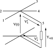
There is a third approach, in which (Figure 3.1c) line sections are added to the parallel 2D TLM node in order to thereby perform the connection with the localized circuit element. The length of the section is set at Δl/2 in order to ensure the synchronism of pulses across the whole TLM network. This technique forces the scattering matrix to be modified in order to take into account the new line section, but it will not be changed for each iteration. On the other hand, the reflection coefficient of the added line section will be recomputed for each iteration, but this implies a single variable (the voltage in the section).
Figure 3.1. A localized circuit element connected to the TLM2D meshing: a) directly connected to a transmission line, b) directly over the node,c) connected to the TLM node by a line section

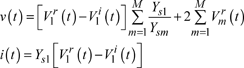
The voltage V(t) on the localized circuit at time t is given by superimposing the incident and reflected voltages propagating along the transmission line section, whereas the current i(t) circulating towards the device is given by their difference, weighted by the admittance Ys of the section:
[3.1] ![]()
The admittance of the line section may be randomly chosen, but a wise choice will enable the computations to be simplified. The value of this admittance is determined in accordance with the scattering matrix of the TLM node loaded with the line section (Figure 3.2). The coefficient S55 of the matrix is equal to (Ys−4)/ (Ys+4). For normalized admittance, Ys = 4, the S55 element of the scattering matrix cancels out and therefore the reflected voltage Vsr is not dependent on the incident voltage Vsi, which is equivalent to decoupling the linear part of the nonlinear part of the device.
The total voltage V(t) and the current i(t) must also satisfy the current-voltage relation which defines the circuit. In general, for a mono-port device, this is expressed by:
[3.2] ![]()
[3.3] ![]()
To simplify, we will only use expression [3.2]. All of the signals are considered to be completely determined by discrete sampling at time intervals Δt, within a limited signal range. The following notations are used:
![]()
In a centered finite difference node network, the following substitutions are given for the time half-step (k-1/2) Δt:
[3.4] 
By substituting the expressions for current and voltage [3.1] into the equation defining the localized circuit and by applying the discretization node network previously defined, a differential equation is obtained which is solved for the unknown kVsi. For the first order circuits, this recursive formula can be expressed in the form:
[3.5] ![]()
For first order circuits, values for Vsi and Vsr will be stored at the previous time step. The computation of new incident pulses in the case of modeling a nonlinear device therefore passes through the solution of a nonlinear equation (F in [3.5] is nonlinear).
The main advantage of this approach is the fact that in choosing appropriate values for the impedance of the added line section, the linear and nonlinear parts of the circuit can be decoupled. For this reason, and also because the interaction of the TLM mesh and the nonlinear circuit (the element) is limited to a single TLM voltage pulse, it is feasible to link the TLM algorithm to other circuit simulators, such as SPICE (simulation program with integrated circuit emphasis).
One disadvantage of this technique is the fact that the line sections added are introducing an additional capacity into the equivalent model of the device, but this error can be offset.
3.1.2. 3D TLM
Here we present one of the two methods in use for the introduction of localized elements into a 3D TLM network, derived from the 2D developments and presented in the previous section, assuming firstly that the localized element occupies a single TLM cell, which does not distort the physical conditions of the problem so long as the dimensions of this circuit element are small in comparison with the other dimensions of the general electromagnetic problem. On the other hand, we are only concerned with the insertion into the SCN node.
3.1.2.1. Mono-port element
3.1.2.1.1. Mono-port element of a volume equal to the TLM cell
The standard SCN node can be fitted with three capacitive line sections (connected in parallel), which modify the three components Ex, Ey and Ez, and three inductive line sections (connected in series), which influence the three components of the magnetic field (Chapter 2). In general, these line sections enable inhomogeneous media to be simulated. If the sub-volume to be modeled consists of an isotropic material, the characteristic admittances and impedances of the line sections are identical.
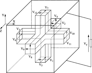
The developments below are made on the hypothesis that the connection of a localized circuit element produces an anisotropic field modification (corresponding to the direction in which the load has been used) and that the element’s dimensions enable it to be assimilated into the volume of a single node. In this case, the modification of the TLM cell will also be anisotropic. In the case described in Figure 3.3, the localized element will only influence component Ey, or even, in terms of TLM “voltages”, the voltage pulses V3, V4, V8 and V11.
Figure 3.3. Connection of a mono-port device to a TLM node: the presence of the device only modifies the voltages in the y direction
As in the 2D case, the technique proposed for modifying these voltages is to add a line section, connected in parallel in the y direction, which, for the general scattering matrix (Chapter 2), corresponds to the case where all line section admittances are null, with the exception of Yy. As in 2D, the choice of appropriate values for normal admittance of the line section enables the incident voltage to be decoupled from that reflected onto the transmission line which joins the device with the SCN node. In the same way that a transmission pulse of 14 in the scattering matrix corresponds with the line section relative to the Ey component, so decoupling will occur at S14,14 = 0, which implies that Yy = 4.
Subsequently, the voltage and current in the circuit are defined respectively as the sum and difference between the incident voltage and the voltage reflected onto the transmission line (see [3.1]). The current-voltage relation which defines the circuit will be replaced by a reflected-incident voltage relation, which is discretized and which, through a recursive relation, enables a new incident voltage to be obtained, which is propagated towards the TLM node (see [3.5]).
3.1.2.1.2. Mono-port element with a higher volume than a TLM cell
The remarks above, regarding anisotropy from the modification of nodes connected to the localized circuit element, remain valid for devices with dimensions greater than a TLM cell. The extent of the device may be in the direction of the voltage drop at the device boundaries or even in the plane perpendicular to the voltage drop at these boundaries.
Let us consider, firstly, the second situation, where the width of the localized circuit element is equivalent to several TLM cells. In this case, the localized element can be considered to be a parallel combination of equivalent identical sub-elements, whose properties can be obtained by the simple application of Kirchhoff’s equations. Each of these elements will be connected to one of the TLM nodes contained in the device volume. This situation is illustrated in Figure 3.4.
Figure 3.4. Equivalent model of the device, containing multiple TLM cells in the plane perpendicular to the voltage drop (xz plane)

With this approach, the behavior of each sub-element is only dependent on the local field corresponding to the TLM cell. This hypothesis is acceptable for most situations and offers the advantage of being easy to implement.
If the length of the component is greater than a TLM cell, the component will be placed over multiple nodes in the direction of the voltage drop at its boundaries and will be decomposed into multiple identical elements connected in series (Figure 3.5). The series decomposition may be induced from the instabilities in the case of strongly nonlinear devices, such as the Gunn or tunnel diodes [CAS 97]. Another disadvantage is the fact that for nonlinear devices, in order to determine the Vmi voltage, a system of nonlinear equations at each time step must be solved.
It is therefore preferable to avoid series element decomposition.
In order to avoid this type of behavior, a new technique must be used for the nonlinear active elements in the 3D TLM mesh. This technique models the active region as a whole, such as a single device in the voltage drop direction, and is dealt with for the other directions by a combination of parallel sub-elements.
The connection between the TLM nodes and the device is always fulfilled with parallel line sections, the voltage at the boundaries of the device being equal to the sum of voltage drops over each line section in the active region. This model is physically equivalent to the arrangement of lines in series, as shown in Figure 3.5. In the interests of simplicity, we are, firstly, going to assume that the width of the device is that of a single TLM node and we will not take its length into account.
Figure 3.5. Device occupying multiple cells in the direction of the voltage drop at the boundaries of the device (y direction)

The procedure used to connect the device explained using [3.5] must take into account the new line section configuration. Equation [3.1] becomes:
[3.6] 
where M is the number of TLM cells used by the device, m indicates the node to which the line section pertains and Ys represents the line section admittance (which is the same for all line sections in the active region). In the example given, Ys = YyY0, when Y0 is the admittance of the TLM lines.
As a result of the series connection of the lines, the same current i(t) flows through the device and the line sections added, which enables all of the incident voltages Vmi(t) to be expressed based on a single one, for example V1i(t). Thus, from the second system equation [3.6]:
[3.7] ![]()
By substituting this relation into the first equation [3.6], the voltage and current over the localized circuit are expressed is such a way as to be dependent on a single unknown V1i (t):
[3.8] 
When these relations are substituted into the current-voltage relation which characterizes the device, they are subsequently discretized. The finite difference equation obtained thus is solved for the unknown V1i (t): incident pulse in the first node used to connect the element into the TLM mesh. The other incident pulses will be determined by using relation [3.7].
For first order circuits, a general recursive formula for calculating the new incident voltage based on the reflected pulses can be expressed as follows:
[3.10] ![]()
Only one nonlinear equation F needs to be solved in order to determine the incident pulses in the nodes connected to the localized elements for each iteration.
In general, when the volume of the device is greater than that of a single TLM cell, a combination of the techniques described in this section is used. The device is firstly divided into equivalent parallel sub-elements which are defined by the same relations as the original device, but with impedances and admittances divided in relation to the number of nodes “covered” by the device volume. Each of the sub-elements is interfaced with a series of nodes, in the voltage drop direction at the device boundaries.
3.1.2.1.3. Mono-port elements in inhomogeneous media
The hypothesis that the connection of a localized element to a SCN node affects a single component of the field (anisotropic modification of the TLM cell) remains valid. In order for the device to be oriented in any Cartesian direction, the SCN node is supplied with three supplementary appropriate admittance lines, a single one of which is effectively used to connect the device, whereas the other two have a null admittance (eventually we can use sections 13–18 if they have not already been used to describe the medium).
The scattering matrix of the new node, which now takes the interaction between the 21 lines (12 transmission lines and nine line sections) into account, is determined in accordance with the charge conservation law. By using the line sections of the localized elements, an incident voltage pulse in the TLM node coming from the TLM node is added to the other voltage pulses from the node. For this, a 21 × 21 matrix is required to model the properties of the medium.
The coefficients of the new matrix are given by:
[3.11] 
where Y is the normalized admittance of the line section for modeling the permittivity of the material, Z is the normalized impedance of the line section for modeling the permeability and Ys is the normalized admittance of the line section of the localized element, which differs based on the device direction (Ysx, Ysy, Ysz). The form of the scattering matrix, modified by the presence of line sections of the localized element, is given in Figure 3.6.
In order to decouple the linear from the nonlinear parts in the behavior of the circuit, the admittance value of the line sections of the device is chosen such that the elements (m) of the scattering matrix, which transfer the reflected voltage into the TLM node and which come back onto the device, are null (Sii = 0, for i = 19 − 21). For example, for a device positioned in the y direction (Figure 3.5), the m20,20 element should be cancelled, which implies that:
[3.12] ![]()

The procedure used to determine the new incident voltages, as explained in the previous sections, is the same in the case of line sections with the same characteristic admittance. For situations in which the localized element is placed in a medium with different permittivities, equations [3.7]–[3.8] become:
[3.13] ![]()
where Ysm is the characteristic admittance of the mth line section of the device.
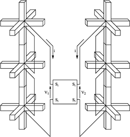
3.1.2.1.4. Two-port elements
For devices such as transistors, the procedure described above can be extended to the modeling of two-port nonlinear devices. In order to simplify the analysis of this procedure, we will assume that the device occupies two rows of adjacent nodes in the z direction and M in the y direction (Figure 3.7). As in the previous cases, the device is modeled as a single element in the voltage drop direction at its boundaries. The device will thus be linked to the row of network nodes which are connected in series in the y direction. In order to be assured that the interaction of the two rows of nodes is only due to the presence of the device connected between them, their line sections in the z direction are terminated by open circuits.
Figure 3.7. Two-port connection of a device in a 3D TLM node network
The localized circuit variables are v1(t), i1(t), v2(t) and i2(t); generally, the behavior of the device is represented by a system of two coupled, nonlinear equations:
[3.15] ![]()
The currents and voltages can also be expressed in terms of the incident and reflected voltages in the arms (the line sections) of the device. Equation [3.9] can be re-written:
[3.16] 
where the indices 1, 2 refer to the two rows of nodes for which these equations are used.
Using the same method for mono-port devices, system [3.16] is substituted into [3.15], which links the voltages and currents in the device; and we use the same principle, as described in the previous section, in order to discretize the resulting equation. In this way, also using relation [3.7] imposed by the series connection of the line sections, we obtain a system of coupled finite difference equations which will describe the incident voltages in the two rows of line sections of the device. For first order circuits, the following expressions are obtained:
[3.17] 
3.1.3. Application example: modeling of a p-n diode
3.1.3.1. Physical model of the diode
The p-n diode is the simplest nonlinear semi-conductor device, consisting of a junction between type p and type n materials (Figure 3.8). When the junction has been polarized, the potential barrier is modified and, as a result, the scattering of carriers between regions. In order to determine the current in the junction based on the bias voltage, the carrier continuity equation, which needs to consider drift currents and electron and hole diffusion currents, must be used.
Figure 3.8. Diode at the p-n junction and its physical mode

By firstly considering the low injection level hypothesis (where the density of majority carriers in each region is not affected by bias) we show that the ideal current-voltage relation governing the behavior of the diode is expressed in the following form:
[3.19] ![]()
where Is is the reverse saturation current, q is the electron charge, k is the Boltzman constant and T is the device temperature in Kelvin. Under reverse polarization conditions the current tends towards −Is.
When the low injection level hypothesis is no longer valid, the difference between the two operating regions is solely the increase in amplitude of the current circulating in the diode. A modification in its variation distribution with the bias voltage of the diode is added to this increase. In order to obtain the model of the diode in the high injection hypothesis, the effects of the storage of the charge in the junction, which transfers the inertia of the diode during a change of direction of the current, will need to be considered. The variation in the space charge relative to the variations in bias voltage results in a dynamic differential capacity, called the “junction transition capacity” and which is given by the following expression:
[3.20] 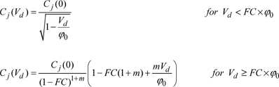
where Cj(0) and ϕ0 are the capacity and potential of the junction at zero bias, m is a coefficient which depends on the junction type (for a linear junction m = 0.33 and for an abrupt junction m = 0.5) and FC is a coefficient used for the change in computation formula for the forward bias capacity (by default FC = 0.5).
When the diode is forward biased, the dominant process is the diffusion of free carriers and the storage of charge is proportional to the total current injected into the junction:
[3.21] ![]()
where τd is the transit time of the diode, which represents the minimum time required to store or free the charge. When a time-variable voltage is applied, the diffusion capacity Cd, given below, must be added to the diode model:
[3.22] ![]()
Other effects may make the diode’s performance different from its ideal behavior. It is incorrect to presume that the carriers are not lost in the depletion region and the actual diode may produce a lower current than that given by [3.19] for low forward bias voltage values. If the voltage applied through reverse bias is too high, then very significant reverse currents may result which may destroy the diode. This results in the consideration of an ohmic resistance due to the voltage drop in the neutral region of the junction, which is necessary for forward bias at a high voltage level. This theory justifies the diode model illustrated in Figure 3.9.
Figure 3.9. Equivalent model of the high level p-n junction diode

3.1.3.2. Diode implantation
The incident pulses in the line sections added to nodes connected to the device (Figure 3.10) are obtained starting from formula [3.9], which is the result of the solution of a system of nonlinear equations which depends on the discrete model chosen.
For the diode model defined above, this is expressed as:
[3.23] 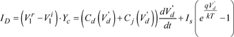
[3.24] ![]()
where:
– Is is the reverse saturation current of the diode;
– V’d is the voltage applied to the p-n junction;
– q is the electronic charge, k is the Boltzmann constant;
– T is the temperature in Kelvin;
– Cj(V’d) and Cd(V’d) are the junction and diffusion capacities (given by equations [3.20] and [3.21]);
– Rs is the series resistance of the diode (Figure 3.9).
A nonlinear system of two equations and two unknowns (Vd’ and V1i) are therefore obtained, which can be solved using traditional software.
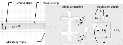
Figure 3.10. Simulation of a micro-strip line loaded by a p-n diode: connection of the diode in the TLM mesh and equivalent circuit of the diode
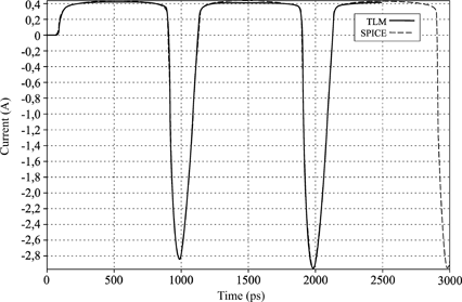
3.1.3.3. Simulation results
Validations have been made in the configuration described in Figure 3.11, using a diode model present in the SPICE library compared with a time regime SPICE simulation, with a 1 GHz sinusoidal excitation signal. The length of the micro-strip line is L = 75 mm. The mesh step is Δl = 0.8 mm and Δt = 1.33 ps. Figures 3.12 and 3.13 compare the results obtained by SPICE and TLM. The graphs are virtually identical, which validates the approach proposed by [BIS 99]
Figure 3.11. Modeled SPICE scheme

Figure 3.12. Current in the diode parallel connected to a 50 Ohm micro-strip line

3.2. Introduction of thin wires [LAR 06]
The modeling of thin wires in electromagnetic computation software, and more specifically the TLM method, is part of the wider area of the modeling of the effect of geometric details on electromagnetic waves. These scenarios are described as being “multiscale” problems and modeling them may be arduous.
Indeed, the use of a very fine mesh which fits the shape of every conductor requires a high number of cells and then leads to a largely prohibitive computation time. Thus multiple numerical processes have been proposed in order to model the interaction between the wires and the surrounding electromagnetic field.
Consideration of the presence of the wire takes place by means of a node incorporating a wider structure. This node transfers the influence of the thin wire onto the surrounding fields, without recourse to a fine mesh. In thin wire modeling, multiple numerical methods have been suggested, whether in FDTD ([HOL 81, UMA 87, MAK 02, BÉR 00, EDE 03]) or TLM ([NAY 90, POR 92, WLO 92, CHO 0l]).
The various TLM models have seen the wire placed between two adjacent cells [WLO 92], or at the center of one of them [NAY 90]. Another TLM school [SEW 03] favors thin wire node development, based on rigorous field theory.
In this paper, we present the arbitrarily oriented thin wire model, developed by Larbi [LAR 06], using the HSCN node, which is the most complete model available today.
3.2.1. Arbitrarily oriented thin wire model
The wire is oriented in any direction ξ defined using the director vector ![]() , where α, β, γ are the director cosines (Figure 3.14).
, where α, β, γ are the director cosines (Figure 3.14).
The length of the wire within the volume of the cell is equal to Δξ.
The system of equations for the wire is given by:
[3.25] 
i indicates the current along the wire and v indicates the voltage on the wire; ![]() is the electrical field along the wire and
is the electrical field along the wire and ![]() is a voltage source per unit length situated at any point along the wire. L, C and Rfil are the inductance, capacitance and resistance respectively of the wire.
is a voltage source per unit length situated at any point along the wire. L, C and Rfil are the inductance, capacitance and resistance respectively of the wire.

3.2.1.1. Current and voltage on the wire
By applying the following normalizations: ![]() , the equation system [3.25] becomes:
, the equation system [3.25] becomes:
[3.26] 
The normalized impedances and a coefficient A are defined:
[3.27] 
System [3.26] becomes:
[3.28] 
The propagation of the current and voltage on the wire is characterized by two pseudo-lines on which voltage pulses V16 and V17, defined as follows, propagate:
[3.29] 
In order to take into account the delays in current, a short-circuit stub is connected to the pseudo-line network. This stub supports the V18 pulses:
[3.30] ![]()
Of course, on this short-circuit stub, we have:
[3.31] ![]()
When the finite difference method is applied to system [3.28] at point (n+1/2, i, j, k), after several manipulations [LAR 06] we arrive at the voltage and current on the wire:
[3.32] 
The source voltage on the wire is expressed as: ![]() . System [3.32] becomes:
. System [3.32] becomes:
[3.33] 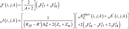
3.2.1.2. Thin wire scattering
The scattering of pulses V16, V17, V18 is obtained by discretizing the voltage and current using the finite difference method, centered at point (n,i,j,k). We obtain:
[3.34] 
The combination of [3.33] and [3.34] gives reflected pulses based on the incident pulses:
[3.35] 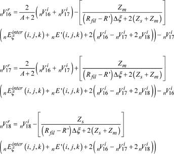
3.2.1.3. Wire inductance and interpolated electrical field
In system [3.35], the lineic inductance of the field and the interpolated electrical field are not defined.
3.2.1.3.1. Wire inductance
The inductance L of the wire defines the interaction between the external electrical field and the current on the wire. For a cylindrical wire of radius a, the inductance L is given by:
[3.36] ![]()
R is the radius of the sphere of influence of the electrical field on the field. The proposition put forward by [EDE 03] is used here: R= (r0+a)/2, where ![]() . This distance is therefore dependent on the mesh. We therefore have:
. This distance is therefore dependent on the mesh. We therefore have:
[3.37] ![]()
3.2.1.3.2. Interpolated electrical field on the wire
We assume that the influence of the electrical field on the wire is null beyond the limit r0. The field on the wire is computed from components Ex, Ey, Ez using a weighted interpolation method:
[3.38] ![]()
where:
– ![]() is the director vector of the wire;
is the director vector of the wire;
– ![]() are the computed electrical field components at the center of the TLM cell;
are the computed electrical field components at the center of the TLM cell;
– g(r) is a weight function;
– the volume V is a sphere of radius r0 encircling the wire.
For continuity conditions, the function g(r) must satisfy the following relations:
[3.39] 
A function fulfilling these conditions is:
[3.40] 
The interpolated field is written:
[3.41] ![]()
The elementary volume is: ![]() and the interpolated field is:
and the interpolated field is:
[3.42] ![]()
where:
[3.43] 
3.2.1.4. Coupling between the electromagnetic field and the current
The influence of the wire on the surrounding electromagnetic field is expressed in Maxwell’s equations by a supplementary term: the current density.
[3.44] 
where σe and σm are the electrical and magnetic conductivities of the medium.
The second equation from the previous system is not modified by the presence of the wire. The first equation is expanded into:
[3.45] 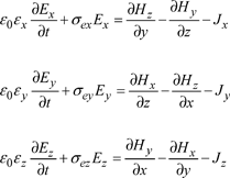
The current density J is based on the radial distance separating the wire from the center of the cell, i.e.:
[3.46] ![]()
g(r) is the weight function defined in section 3.2.1.3.2.
The distributed current density is approached by the relation:
[3.47] ![]()
with N = i + j + k the base functions of the Cartesian system.
By normalizing the coordinates x, y, z and t: x = uX, y = vY, z = wZ and t = (Δt/2c)T, (the normalized electrical fields E and normalized magnetic fields H are the voltage dimensions), [3.45] becomes:
[3.48] 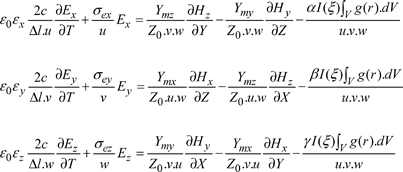
with the following normalized admittances:
[3.49] ![]()
as well as:
[3.50] 
The equations of [3.48] become:
[3.51] 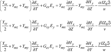
where: ![]() , I is the current in the wire and ℑ is defined by expression [3.43]. Maxwell’s equations for the magnetic field are not modified by the current on the wire and invoke the magnetic conductivities which, once normalized, occur with the equations in the following form:
, I is the current in the wire and ℑ is defined by expression [3.43]. Maxwell’s equations for the magnetic field are not modified by the current on the wire and invoke the magnetic conductivities which, once normalized, occur with the equations in the following form:
![]()
By applying the finite difference method to point (n, i, j, k) in expressions [3.51], following a number of manipulations [LAR 06], we obtain the expression for reflected voltages, based on the incident pulses. These are divided into three parts:
– The 12 HSCN node pulses:
[3.52] 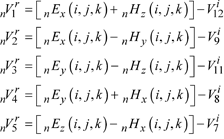

– The 3 open circuit stubs:
[3.53] 
– The 2 pulses and the short-circuit stub linked to the wire:
[3.54] 
The scattering matrix from Figure 3.15 is then obtained. In this table, the index a in the quantities aα, bα, and dα represent values xyz in the order indicated in the 1st column.
The various coefficients of the matrix are defined as follows:
[3.55] ![]()
[3.56] ![]()
[3.58] ![]()
[3.59] ![]()
[3.60] ![]()
[3.61] ![]()
The coefficients A, Zm, Zs, and Yf are:
– A, the constant, taking into account losses in the medium,
[3.62] ![]()
– Zm, the impedance encountered by the pulses on the wire,
[3.63] ![]()
– Zs, the characteristic impedance of the short-circuit stubs,
[3.64] ![]()
– Yf, the normalized admittance of the wire,
[3.65] ![]()

3.2.2. Validation of the arbitrarily oriented thin wire model
Validation of the thin wire model is performed on a dipole consisting of a wire 41 m in length and 1 cm in diameter. Mesh is uniform, with u = v = w = 10 mm. The computation of the input impedance of this dipole in various orientations enables the algorithm previously explained to be tested. This impedance must be independent of the orientation and of course equal to the theoretical value. Moreover, the various resonance frequencies are also independent of orientation. Since the wire is parallel to the Ox axis (t00), it is subject, in the first instance, to movements in the yOz plane, with steps 0.25v (t25) and 0.50v+0.50w (t55) (Figure 3.16a). The other series of transformations consists of making it carry out rotations of 27° (r27) and 45° (r45) in the xOy plane (Figure 3.16b).
Figure 3.16. Dipole configurations

This dipole is fed at its center using the localized voltage source, which is integrated with the wire. The excitation has the appearance of a Gaussian pulse:
[3.66] 
The TLM simulations carried out have the following characteristics:
| Computation volume: | 27 × 67 × 27 nodes |
|---|---|
| Cell dimensions Δl: | 1 m |
| Number of cells in the PML: | 10 |
| Excitation: | [2 MHz; 24 MHz] |
| Number of processors: | 8 |
| Number of iterations: | 2,000 |
Figure 3.17. Input resistance of the dipole obtained using thin wire modeling

Figure 3.17 enables a visualization of the real part of the input impedance of the dipole for the five configurations from Figure 3.16. There is no difference between any of these various configurations. Moreover, the anti-resonance frequencies and the maximum amplitudes of the input resistance conform to those from the method of moments (MoM) used for the purposes of comparison.
Table 3.1 summarizes the values for the half-wave resonance frequency, as well as those for the various simulated cases. The relative error between δf0 and δZTLM is computed by taking the theoretical values as a reference: f0 = 3.66 MHz and Z = 73 Ω.
Table 3.1. Frequencies and resistances of the half-wave resonance of the dipole

The relative errors obtained for resonance frequencies are less than 1.5%, which is quite acceptable and thus validates the method.