Chapter 5
Patterning with Self-Assembling Block Copolymers 1
5.1. Block copolymers: a nano-lithography technique for tomorrow?
Since 1960, the microelectronics industry has witnessed enormous progress focused essentially on the development and application of Metal Oxide Semiconductor (MOS) transistor technologies. Indeed, whereas in 1962 the first integrated circuit included two transistors, today the most powerful microprocessors are composed of several tens of millions of MOS transistors per chip (e.g. 42 million for Intel's Pentium 4). This rapid expansion of microelectronics is driven by the perpetual requirement to manage and store larger quantities of data on increasingly smaller supports, with less energy consumption. This incessant reduction of device dimensions will soon reach the limits of conventional fabrication processes and traditional technologies, such as optical lithography and etching, and will probably not be able to create high density objects of a size c.18 nm, the length predicted for transistors in 2018 [ITR 01]. In this context, the use of block copolymer (BCP) thin films seems to be a powerful alternative for quite specific applications to overcome the intrinsic limitations of traditional lithographic techniques. This technology, based on the self-organization of polymeric chains similar to conventional polymer photoresist chains used in semiconductor fabrication, allows the realization of regular patterns whose dimensions cannot be achieved by optical lithography processes. After decades of being of only secondary importance, as reflected by an almost negligible number of publications on the subject, the capacity of BCPs to self-assemble into periodic morphologies is likely to play a key role in nanotechnological applications in the future. The utilization of the BCP technique to obtain lithographic masks was first proposed in 1995 by Mansky [MAN 95], and appears today as one of the technological solutions to generate localized uniform objects with low dimension (~20 nm) and high density (~1011/cm2).
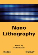
Block copolymers are a specific type of polymer and can be classified as soft matter. They are composed of at least two chemically different polymer fragments ("blocks") which are covalently linked. Generally, copolymers are flexible and can bend at monomer junctions, leading to a great architectural diversity, examples of which include linear copolymers, graft copolymers and star copolymers [OHT 86]. When only two subchains of different monomers, A and B, are bound covalently to each other, a diblock copolymer is formed. A simple linear AB diblock copolymer chain (called: PA-b-PB) is composed of fN polymer A segments and (1-f )N polymer B segments, linked at one end together by a covalent bond, where N denotes the degree of polymerization and fthe fraction of block Ain the chain. The product χN controls the tendencyof the Aand Bblocks to separate, where χ is the Flory-Huggins segmental interaction parameter. At sufficiently large values (i.e. χN> 10.5), the A andB blocks become immiscible and formperiodically separated nanodomains [OHT 86]. Depending on the composition, f, diblock copolymers can organize into several equilibrium structures: lamellae, hexagonally ordered nanodomains, bicontinuous cubic gyroids, or a body-centered-cubic lattice of spheres (see Figure 5.1) [MAT 94]. The periodicity of these structures is determined by a competition between the interfacial tension and the entropic penalty for stretching different blocks in order to maintain a uniform segment density [MAT 96].
Figure 5.1. Schematic representation of diblock copolymer phases as a function of f: (S) spherical; (C) cylindrical; (G) gyroid; (L) lamellar; (G’) inverse-gyroid; (C’) inverse-cylindrical; (S’) inverse-spherical phases [LI 05]
BCP thin films only allow two pattern geometries to be obtained which can be used as lithographic masks: line/space or circular nanodomain patterns. The gyroid structure (Figure 5.1) is not adapted for lithographic applications. In practical terms, block copolymer templates presenting a monolayer of cylindrical nanodomains which are parallel to the substrate, or a lamellar phase oriented perpendicularly to the substrate, could be used to obtain masks allowing the transfer of striped line/space patterns. Alternatively, thin films presenting cylindrical nanodomains perpendicular to the substrate, or a monolayer of spherical nanodomains, can be used to fabricate circular nanopatterns.
Although only line/space or circular nanodomain patterns could be achieved by using BCP as a lithographic mask, this technique will be able, in the long run, to supplant conventional lithography for the realization of several technological applications, such as for:
– the realization of increasingly small Dynamic Random Access Memory (DRAM) cells presenting shallow trench array capacitors with a higher capacitance than planar capacitors with the same dimensions [BLA 04a],
– the elaboration of nanocrystal floating-gate memories which offer greater robustness than conventional Flash memory devices when dimensions are reduced, as imposed by the demand of an ever higher integration density [BLA 07].
The utilization of diblock copolymer masks could be interesting for other applications where dense patterns of discrete objects are needed. Examples include quantum dots or nanopillars [PAR 97, AIS 08], the fabrication of high density magnetic recording devices [CHE 01] and the fabrication of nanowires [THU 00a].
Unfortunately, the organization of patterns in BCP films is often accompanied by the presence of isolated defects or an array of defects which can be prejudicial to the applications cited above. Thus, block copolymer self-assembly and its defect formation and diffusion have to be understood and perfectly controlled.
5.2. Controlling self-assembled block copolymer films
Many thin film studies performed during the last years have focused on asymmetric diblock copolymers as nanolithographic templates. As already mentioned, two pattern types can be generated by a self-assembling diblock copolymer film: striped line/space patterns and circular patterns, depending on the morphology of the self-assembling BCP film. Below, we describe the formation of periodical circular patterns, knowing that striped line/space patterns globally present a similar behavior.
Remember that these circular 2D-periodic hexagonally organized patterns can be obtained either (1) from a monolayer film organized into close-packed spheres, or (2) from a thin film containing an array of cylindrical nanodomains oriented vertically to the substrate. Segalman et al. [SEG 03] studied the organization of films formed by a monolayer of spheres and found that hexagonal block copolymer patterns consist of well-organized areas (grains) separated by boundaries (arrays of topological defects) and discrete defects. In these lattices, isolated defects are called “disclinations” or orientational defects since they affect the orientational 2D lattice order. If the defective nanodomain is pentacoordinated the defect is called “negative disclination”, and it is called “positive disclination” if the nanodomain is heptacoordinated. If two disclinations of different sign are paired (7-5) a defect called a “dislocation” is formed.
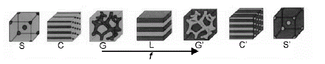
These defects will now be illustrated using a hexagonal lattice obtained by using a thin diblock copolymer film composed of polystyrene (PS) and polymethylmethacrylate (PMMA), referred to as PS-b-PMMA. Figure 5.2(a) is a Scanning Electron Microscopy (SEM) image of a typical 2D hexagonally organized array of holes in a PS matrix that Aissou et al. [AIS 07a] obtained after annealing a PS-b-PMMA layer at 200°C under vacuum (10-2 mbar) for 72 h and removing the PMMA blocks using a deep UV light treatment. The porous PS template is composed of different grains whose nanodomains (dark on the image) are oriented vertically to the surface and have a diameter of about 20 nm and a periodicity of about 40 nm. Figure 5.2(b) shows the associated Delaunay triangulation of the SEM image presented in Figure 5.2(a).
Figure 5.2. (a) Typical SEM image of a porous PS film obtained after annealing at 200°C under vacuum for 72 h, and removal of PMMA cylinders. (b) The associated Delaunay triangulation of the porous PS film presented in (a). Cylinders with seven and five neighbors are indicated by light and dark grey dots, respectively. Dislocations formed by a pair of 5-7 disclinations are indicated by connecting bars. Disclinations consisting of a hepta- or pentacoordinated nanodomain are indicated by a light or dark grey encircled star, respectively. Reproduced and adapted with permission from Macramolecules [AIS 07a]
In Figure 5.2(b), we can observe well-organized grains corresponding to regions where all cylinders are 6-fold coordinated; these grains are delimited by defects. Heptacoordinated and pentacoordinated nanodomains (light and dark grey dots,respectively) correspond to defects which separate grains presenting an anisotropic shape and a specific orientation. Disclinations consisting of a penta- or heptacoordinated nanodomain are indicated by a dark or light grey encircled star, respectively (Figure 5.2(b)), and dislocations are indicated by a connecting bar. Vega et al. [VEG 05] noted that disclinations present in hexagonal patterns, correlate to high angle grain boundaries i.e. with an angle disorientation between two adjacent grains higher than 15°. Hammond et al. [HAM 03] studied topological defects in films forming cylindrical nanodomains oriented vertically to the surface, and their study revealed that the local stress field of the lattice influences the pore dimensions and that the mean nanodomain area varies as a function of the degree of coordination of the pore. In the PS-b-PMMA diblock copolymer case described above, a disparity of pore areas between 5-fold, 6-fold and 7-fold coordinated nanodomains was evidenced [AIS 07a], a disparity which is higher among the 7-fold sites than among the 5-fold or 6-fold sites. This strong variation is induced by a deformation of the unit cell (a pore plus its PS corona) from an isotropic shape to an anisotropic shape (see Figure 5.2(a)). This phenomenon induces a variation in the object dimensions fabricated with block copolymer patterns. An example is shown in Figure 5.6(b).
The presence of defects delimiting well-organized areas and the variation of the diameter of the nanodomains, attributed to a local constraint of the array [OHT 95], are prejudicial limitations for nanotechnological applications of these films. The nucleation-growth mechanism of macroscopic grains has been extensively debated over the last decade in order to improve the 2D order of the film [SEG 03, VEG 05, PIG 07, HAR 04]. Theoretical [YOK 02] and experimental [VEG 05, HAR 04, HAR 00] studies have focused on the evolution of these topological defects as a function of time, and have reported that the number of dislocations and disclinations decreases when the annealing time increases. In the case of lattices containing a monolayer of spheres, Vega et al. [VEG 05] concluded that this diminution is due either to a mechanism of grain rotation or to a mechanism of annihilation of low angle grain boundaries.
Agreeing with these models, Aissou et al. [AIS 07a] proposed a microscopic mechanism, which explains the diffusion of the dislocations during annealing for cylindrical nanodomains organized in a hexagonal lattice. This mechanism, which is based on the division of deformed heptacoordinated cylinders into two distinct cylinders, allows the displacement and the new orientation of the dislocations (which are at the origin of the reduction of the density of the topological defects) to be explained.
Even if the number of topological defects decreases during the annealing time and their disappearance allows a homogenization of the size of the nanodomains, the mechanisms at the origin of this diminution are generally slow. For example, an annealing time of several weeks would theoretically be necessary to obtain a perfect organization of the domains on a surface of 1 cm2. Although several methods, such as solvent annealing [KIM 04], allow a better organization of nanodomains to be obtained locally than by thermal annealing, so far only thermally processable materials have a good chance of becoming adopted technology.
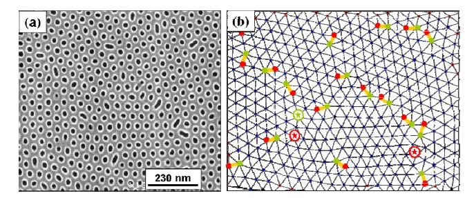
Figure 5.3. (a) Schematic representation of a BCP thin film deposited on a patterned substrate: (a) before (1) and after (2) annealing; (b) Plan-view SEM images of a PS template presenting vertically oriented cylinders in a groove obtained after removal of the PMMA; (c) Plan-view SEM image of a PS template presenting horizontally oriented parallel cylinders in grooves obtained after removal of the PMMA
In order to increase the kinetics of defect elimination, several studies have shown that partial or total confinement of the film would allow this problem to be solved. Among these techniques one can cite nanoimprint lithography [LI 04], surface nanopatterning by local chemical modification [STO 06, EDW 06] or graphoepitaxy [SEG 01, XIA 05] which consists of creating trenches in the substrate with conventional photolithography/etching processes. The idea of this last technique is that the confinement of the film in the trench induces a strong constraint on the nanodomains formed which are then forced to organize in an optimal way (without defects). It has been shown, in the case of spherical nanodomains, that they first form close to the sidewalls and then form inwards so that the film is well ordered across the width of the grooves and along their axes [CHE 02, CHE 06, SEG 03]. Graphoepitaxy has also been shown to be an effective strategy for ordering cylinder-forming block copolymers with domains oriented either perpendicular [XIA 05, LI 04] (e.g. Figure 5.3(b)) or parallel [SUN 04] (e.g. Figure 5.3(c)) to the substrate, and in geometries more complex than parallel grooves such as circles [BLA 04b] and bends [SUN 04].
These techniques allow an improvement in the order of the nanodomains formed in thin films which have to be integrated in fabrication processes for nanotechnological applications whose feasibility has already been demonstrated and which have the potential to be commercialized. It has already been demonstrated that diblock copolymer thin films organized using graphoepitaxy can be used for the fabrication of magnetic storage media [NAI 02, XIA 05] or nanowire field effect transistors (FETs) [BLA 05].
5.3. Technological applications of block copolymer films
The realization of etching masks with a high BCP film thickness h is essential because of the low selectivity of organic films with respect to the inorganic material (SiO2, SiN, etc.) to be etched. This is why films presenting an array of vertically oriented block copolymer cylinders seem to be more advantageous for the realization of discrete circular nanopatterns compared to films presenting an array of spheres, because they present, a priori, no thickness limitation.
Indeed, a film composed of spherical nanodomains must have an initial thickness of roughly the natural monolayer thickness h0 due to the fact that the spheres of a second layer would be shifted with respect to the spheres of the lower one (phase S and S’, Figure 5.1) which would prevent the use of the film as a mask. This can cause an absence of objects on 200 mm devices in zones where the film is thicker than h0, since thickness variations of some nanometers always occur in an uncontrolled way at this scale. For this reason, the following discussion concerns pattern transfer using cylindrical nanodomains.
For lithography applications of films presenting a cylinder or lamella array of nanodomains, oriented perpendicular to the surface, it is essential that the substrate surface develops similar interaction energies with the various blocks constituting the polymer chains. In other words, it is crucial that the interaction energies between the surface and each copolymer block are modified, e.g. by using a chemical treatment, so that surface energies become equivalent.
BCP films composed of spherical nanodomains do not require a particular surface treatment if they are used as a lithographic mask, because only one of the phases is in contact with the substrate.
Before diblock copolymer films can be used to transfer a structure, one of the phases has to be selectively removed. Details of some of the physical and/or chemical processes which allow this to be done, in order to obtain a nanolithographic mask, are detailed below.
Thurn-Albrecht et al. demonstrated that it is possible to remove the polymethylmethacrylate (PMMA) block from a PS-b-PMMA system by using UV light [THU 00b]. The UV radiation induces a preferential PMMA phase degradation via chain scission, whereas PS is crosslinked and becomes insoluble leaving a porous PS template. Using an ozone treatment, Park et al. [PAR 97] showed that polyisoprene (PI) and polybutadiene (PB) blocks in PS-b-PI and PS-b-PB systems could be selectively removed. This is due to the ability of ozone to cleave carbon-carbon double bonds (C=C) which are contained in polydienes. For these same systems, Park et al. noted that it is possible to reverse the mask, i.e. to selectively etch the PS block by staining the carbon-carbon double bonds with OsO4. Recently, for a poly(styrene-b-dimethylsiloxane) system (PS-b-PDMS), a selective degradation of the PS block was observed by using a two step plasma etching process: (i) a CF4 plasma followed by (ii) a O2 plasma [JUN 07]. First, the fluorinated chemistry allows the removal of the air/polymer PDMS contact layer while the O2 plasma selectively etches the carbon skeleton of the PS block copolymer. Finally, we can quote the use of systems containing polyferrocenyldimethylsilane (PFS). These systems presenting a Si and Fe based skeleton have a strong resistance to O2 etching. Generally, in the literature, this type of polymeric chains is found associated to a PS block or to a PI block, i.e. blocks which can be easily removed by O2 plasma etching [LAM 00, CHE 03].
In other words, the choice of the diblock chains is very important to allow the selective removal of one block with respect to the other. We will now illustrate some of the objects obtained using diblock copolymer films presenting vertical nanodomains.
BCP films can be used either as etching masks to transfer a pattern directly to the underlying substrate, or as deposition masks to organize dots or lines of different materials on the substrate surface. It is also possible to combine etching and deposition by first transferring the pattern to the substrate by etching and then depositing material dots or lines in the etched holes or trenches. The polymer template can also be reversed by using it for the deposition of dots followed by liftoff. These dots can then be used as a hard-mask to generate substrate nanopillars by plasma etching.
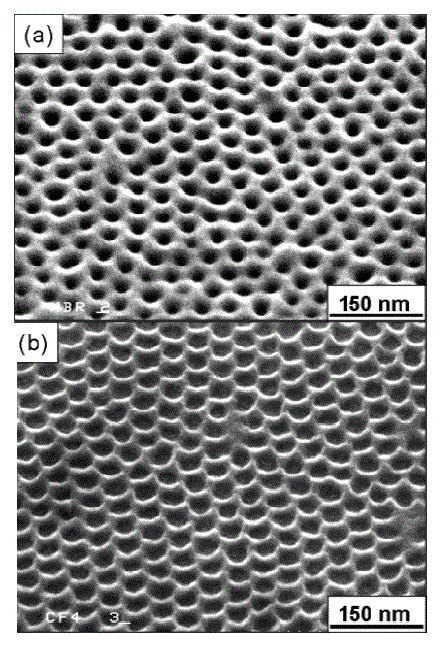
Figure 5.4. SEM images of an array of organized holes in a silicon oxide layer obtained by using a PS mask for plasma etching with different chemistries: (a) an HBr plasma allows a mean hole diameter of about 20 nm to be achieved, and (b) a CF4 plasma allows a mean hole diameter of about 30 nm to be achieved. Reproduced and adapted with permission from Surface Science [AIS 07b]
If a diblock copolymer template is used as deposition mask, a low temperature process, such as physical vapor deposition (PVD), has to be used because the polymer template is not resistant to the high temperature of a Chemical Vapor Deposition (CVD) process.
The first pattern transfers using a BCP mask were carried out by Park et al. [PAR 97] by depositing various PS-b-PB films, whose compositions were adjusted to obtain a monolayer of spheres or lying cylinders, onto silicon nitride substrates (Si3N4). Park et al. have shown that it is possible to transfer holes, trenches or pillars to the Si3N4 substrate. Similar results were reported for the PS-b-PI system. Proceeding in the same way, Harrison et al. [HAR 97] presented evidence of the possibility to create holes in a germanium layer. For example, Figure 5.4 presents an array of organized holes in a 10 nm SiO2 layer obtained using a PS porous template as an etching mask. The mean hole diameter can be tuned by adapting the chemistry of the etching plasma [AIS 07b].
The utilization of a monolayer of spheres or horizontal cylinders as a mask for metal deposition has not been successful, due to the low depth of holes or trenches in the mask, which makes the liftoff very difficult. In order to overcome this problem, Park et al. [PAR 01] intercalated a polyimide layer between the substrate and the Si3N4 layer. The use of this trilayer (PS/Si3N4/polyimide) allows the realization of a mask with deep holes, thus facilitating the liftoff step after the metal deposition. Eventually, Park et al. obtained an organized pattern of Ti/Au dots. Nevertheless, this spectacular result requires a huge number of process steps.
A real revolution for BCP lithography was marked by the realization of vertical cylinders in a controlled manner. Film thickness is no longer limited to a monolayer of spheres, and there is no residual PS layer between the substrate and the nanodomains of the mask, as in the case of the spherical nanodomain phase. However, it is necessary to prevent the preferential adsorption of one of the two blocks constituting the copolymer film. Mansky et al. [MAN 97] showed that it is possible to control interfacial energies and wetting behavior of polymers by grafting random copolymer brushes on the silicon surface. In order to obtain cylinders oriented perpendicular to the substrate, Thurn-Albrecht et al. [THU 00b] used this method to obtain the same surface behavior for PS and PMMA. By using the random PS-r-PMMA copolymer, Thurn-Albrecht et al. obtained PS-b-PMMA films with vertically-oriented PMMA cylinders after annealing. Then, after exposure to UV light and immersion in an acetic acid developer, an array of holes in a PS template was obtained. Guarini et al. [GUA 01, BLA 01] were the first to transfer this type of mask to a SiO2 layer by CHF3 Reactive Ion Etching (RIE), and then to an Si substrate by SF6 RIE. The hole pattern obtained can be used to enhance the charge storage capacity of a metal-oxide-semiconductor (MOS) capacitor without increasing the lateral dimensions. This could allow DRAM memory cells to be manufactured with a higher capacity than that obtained with planar technology. Guarini et al. [GUA 02] also realized a pattern reversal by depositing a silicon nitride layer by rapid thermal chemical vapor deposition onto a porous SiO2 mask obtained using diblock copolymer technology. Then, the SiO2 template and the silicon nitride on top of it were removed leaving a mask of silicon nitride dots on the substrate. This mask was then used to obtain silicon nanopillars by etching.
Guarini et al. [GUA 03] also demonstrated the possibility of fabricating a nanocrystal flash memory by using a diblock copolymer mask for the deposition of Si dots, capping them with a 7 to 12 nm thick control oxide layer, and then depositing a polysilicon gate.
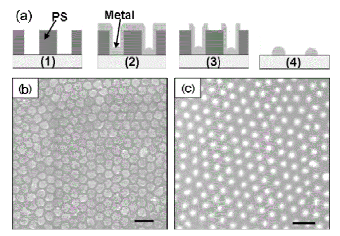
In order to illustrate the use of a PS porous template as a deposition mask, Figure 5.5 presents an organized metal dot array obtained by a lift-off technique.
Figure 5.5. (a) Schematic process flow diagram for metal dot fabrication by lift-off technique: (1) Ps porous template,(2) after metal deposition onto the mask, (3) after an Ar plasma to selectively remove the excess metal on the top PS layer and (4) after an O2 plasma to remove the residual polymer and side-walls of metal-coated PS. (b) SEM image of a 5 nm thick Pt dot array on SiO2.(c) SEM image of a 5 nm thick Au dot array on SiO2. The black bars correspond to 80 nm
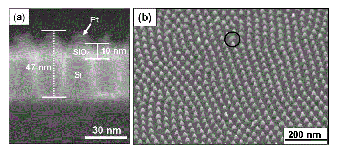
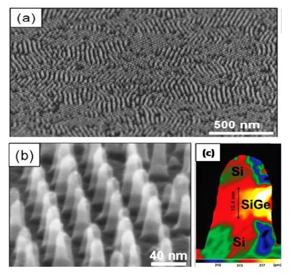
These metal dot arrays have been used as hard-masks to generate (i) organized Si nanopillars by HBr/Cl2 plasma etching (see Figure 5.6) [AIS 07a] or (ii) to fabricate organized Si0.8Ge0.2 quantum dots in Si nanopillars by using a Cl2/O2 plasma to etch an Si/SiGe multilayer (see Figure 5.7) [AIS 08]. These kinds of quantum dots could serve as building blocks for future optoelectronic applications.
In order to obtain perfectly organized metallic dots, other studies were carried out simultaneously by using macromolecules containing a PFS block. In particular, the PI-b-PFS system was used to obtain Si-Fe oxide dots by O2 RIE, after the organization of PFS spheres in a PI matrix [LAM 00]. Indeed, the O2 RIE process allowing the removal of the PI phase induces a partial oxidation of the PFS. Taking the etching robustness of the oxidized spheres into account, these spheres were used to etch multi-layers (PFS/ SiO2/W/Co/Si) in order to obtain W dots on a Co layer or magnetic Co dots on a Si layer [CHE 01].
Figure 5.6. SEM images of nanopillars obtained after transfer of a Pt dot mask to a substrate by etching with an HBr/Cl2 plasma: (a) Profile image showing the different layers of the pillars (5nm Pt/10 nm SiO2/ Si) and (b) enlarged image view showing a hexagonal array. The black circle shows a deformed nanopillar due to the presence of a defect in thePS mask. Reproduced and adapted with permission from Macramolecules [AIS 07a]
To conclude, it has been shown throughout this chapter that it is possible to use thin diblock copolymer films as etching or deposition mask to fabricate discrete objects (holes, dots and pillars) with small dimensions and high density which cannot be obtained by conventional optical lithography and plasma etching. These objects are building blocks for more complex applications (flash memories, DRAM, LED, nanowire FET, etc.). It is preferable to use films with vertically organized nanodomains (cylinders and lamellae) because they present no thickness limitation. This is important for etching processes where the selectivity with respect to the substrate is low. Furthermore, they allow the critical lift-off step to be performed if the template is used as a deposition mask. The choice of the blocks constituting the block copolymer chains is also very important and is guided by the fact that one block has to be removed (chemical and/or physical etching) selectively with respect to the other, in order to obtain a nanolithographic mask.
Figure 5.7. (a) and (b) SEM images of Si nanopillars containing SiGe at different magnifications obtained after a Pt dot mask transfer to the substrate having an alternation of 10 nm thick Si and Si0.8Ge0.2 layers by using a Cl2/O2 etching plasma. (c) (111) interplanar distance map in pm obtained from a single nanopillar by using Geometrical Phase Analysis. Reproduced and adapted with permission from Chemistry of Materials [AIS 08]
The presence of defects in the films has also been discussed. It is imperative that defects are limited or suppressed to be able to use these films as a technological solution for future microelectronics. Topological defects (dislocations and disclinations) are difficult to control and curing mechanisms have very slow kinetics. A solution to overcome this problem is to partially or totally confine the BCP film by using nanoimprint lithography, local chemical modification or graphoepitaxy techniques in order to accelerate the kinetics of defect elimination.
5.4. Bibliography
[AIS 07a] AISSOU K., BARON T., KOGELSCHATZ M., PASCALE A., “Phase behavior in thin films of cylinder-forming diblock copolymer: Deformation and division of heptacoordinated microdomains”, Macromolecules, 40, 5054, 2007.
[AIS 07b] AISSOU K., BARON T., KOGELSCHATZ M., GENTILE P., “Self-assembled block polymer templates as high resolution lithographic masks”, Surf; Sci., 601(13), 2611, 2007.
[AIS 08] AISSOU K., BARON T., KOGELSCHATZ M., DEN HERTOG M., ROUVIERE J. L. HARTMANN J. M., PELISSIER B., “Fabrication of well-organized and densely packed Si nanopillars containing SiGe nanodots by using block copolymer templates”, Chem. Mater., 20, 6183, 2008.
[BLA 01] BLACK C. T., GUARINI K. W., MILKOVE K. R., BAKER S. M., RUSSELL T. P., TUOMINEN M. T., “Integration of self-assembled diblock copolymers for semiconductor capacitor fabrication”, Appl. Phys. Lett., 79, 409, 2001.
[BLA 04a] BLACK C. T., GUARINI K. W., ZHANG Y., KIM H. J., BENEDICT J., SIKORSKI E., BABICH I. V., MILKOVE K. R., “High-capacity, self-assembled metal–oxide–semiconductor decoupling capacitors”, IEEE Electron Device lett., 25(9), 622, 2004.
[BLA 04b] BLACK C. T., BEZENCENET O., “Nanometer-scale pattern registration and alignment by directed diblock copolymer self-assembly”, IEEE Trans. Nanotech., 3(3), 412, 2004.
[BLA 05] BLACK C. T., “Self-aligned self assembly of multi-nanowire silicon field effect transistors”, Appl. Phys. Lett., 87, 163116, 2005.
[BLA 07] BLACK C. T., RUIZ R., BREYTA G., CHENG J. Y., COLBURN M. E., GUARINI K. W., KIM H.-C., ZHANG Y., “Polymer self assembly in semiconductor microelectronics”, IBM J. Res. & Dev., 51 (5), 605, 2007.
[CHE 01] CHENG J. Y., ROSS C. A., CHAN V. Z., THOMAS E. L., LAMMERTINK G. H., VANSCO G. J., “Formation of a cobalt magnetic dot array via block copolymer lithography”, Adv. Mater., 13(15), 1174, 2001.
[CHE 02] CHENG J. Y., ROSS C. A., THOMAS E. L., SMITH H. I., VANCSO G. J., “Fabrication of nanostructures with long-range order using block copolymer lithography”, Appl. Phys. Lett., 81, 3657, 2002.
[CHE 03] CHENG J. Y., ROSS C. A., THOMAS E. L., SMITH H. I., VANSCO G. J., “Templated self-assembly of block copolymers: effect of substrate topography”, Adv. Mater., 15(19), 1599, 2003.
[CHE 06] CHENG J. Y., ZHANG F., SMITH H. I., VANCSO G. J., “Pattern registration between spherical block-copolymer domains and topographical templates”, Adv. Mater., 18, 597, 2006.
[EDW 06] EDWARDS E. W., STOYKOVICH M. P., NEALEY P. F., SOLAK H. H., “Binary blends of diblock copolymers as an effective route to multiple length scales in perfect directed self-assembly of diblock copolymer thin films”, J. Vac. Sci. Technol. B, 24(1), 340, 2006.
[GUA 01] GUARINI K. W., BLACK C. T., MILKOVE K. R., SANDSTROM R. L., “Nanoscale patterning using self-assembled polymers for semiconductor Applications”, J. Vac. Technol. B, 19, 2784, 2001.
[GUA 02] GUARINI K. W., BLACK C. T., ZHANG Y., KIM H., SIKORSKI E. M., BABICH I. V., “Process integration of self-assembled polymer templates into silicon Nanofabrication”, J. Vac. Technol. B, 20, 2788, 2002.
[GUA 03] GUARINI K. W., BLACK C. T., ZHANG Y, BABICH I. V., SIKORSKI E. M., GIGNAC L. M., “Low voltage, scalable nanocrystal FLASH memory fabricated by templated self assembly”, IEEE, IEDM 03-541, 22.2.1, 2003.
[HAM 03] HAMMOND M. R., SIDES S. W., FREDRICKSON G. H., KRAMER E. J., RUOKOLAINEN J., HAHN S. F., “Adjustment of block copolymer nanodomain sizes at lattice defect sites”, Macromolecules, 36, 8712, 2003.
[HAR 97] HARRISON C., PARK M., CHAIKIN P. M., REGISTER R. A., ADAMSON D. H., “Lithography with a mask of block copolymer microstructures”, J. Vac. Technol. B, 16(2), 544, 1997.
[HAR 00] HARRISON C. K., ADAMSON D. H., CHENG Z., SEBATIAN J. M., SETHURAMAN S., HUSE D. A., REGISTER R. A., CHAIKIN P. M., “Mechanisms of ordering in striped patterns”, Science, 290, 1558, 2000.
[HAR 04] HARRISON C. K., ANGELESCU D. E., TRAWICK M. L., CHENG Z., HUSE D. A., CHAIKIN P. M., VEGA D. A., SEBASTIAN J. M., REGISTER A., ADAMSON D. H., “Pattern coarsening in a 2D hexagonal system”, Europhys. Lett., 67(5), 800, 2004.
[ITR 01] International Technology Roadmap for Semiconductors, http://www.itrs.net/links/2001itrs/Home.htm, 2001.
[JUN 07] JUNG Y. S., ROSS C. A., “Orientation-controlled self-assembled nanolithography using a polystyrene-polydimethylsiloxane block copolymer”, Nano Lett., 7(7), 2046, 2007.
[KIM 04] KIM S. H., MISNER M. J., XU T., KIMURA M., RUSSELL T. P., “Highly oriented and ordered arrays from block copolymers via solvent evaporation”, Adv. Mater., 16(3), 226, 2004.
[LAM 00] LAMMERTINK G. H., HEMPENIUS M. A., VAN DEN ENK J. E., CHAN V. Z., THOMAS E. L., VANSCO G. J., “Nanostructured thin films of organic-organometallic block copolymers: One-step lithography with poly(ferrocenylsilanes) by reactive ion etching”, Adv. Mater., 12(2), 98, 2000.
[LI 04] LI H. W., HUCK W. T. S., “Ordered block-copolymer assembly using nanoimprint lithography”, Nano Lett., 4(9), 1633, 2004.
[LI 05] LI M., COENJAERTS C. A., OBER C. K., “Patternable block copolymers”, Adv. Polym. Sci., 190, 183, 2005.
[MAN 95] MANSKY P., CHAIKIN B., THOMAS E. L., J. Mater. Sci. 30, 1987, 1995.
[MAN 97] MANSKY P., LIU Y., HUANG E., RUSSELL T.P., HAWKER C., “Controlling polymer-surface interactions with random copolymer brushes”, Science, 275, 1458, 1997.
[MAT 94] MATSEN M. W., SCHICK M., “Stable and unstable phases of a diblock copolymer melt”, Phys. Rev. Lett., 72(16), 2660, 1994.
[MAT 96] MATSEN M. W., BATES F. W., “Origins of complex self-assembly in block copolymers”, Macromolecules, 29(23), 7641, 1996.
[NAI 02] NAITO K., HIEDA H., SAKURAI M., KAMATA Y., ASAKAWA K., “2.5-inch disk patterned media prepared by an artificially assisted self-assembling method”, IEEE Trans. Magn., 38(5), 1949, 2002.
[OHT 86] OHTA T., KAWASAKI K., “Equilibrium morphology of block copolymer melts”, Macromolecules, 19(10), 2621, 1986.
[OHT 95] OHTA T., IWAY Y., Ito A.., Gunton J. D., Physica B, 213, 672, 1995.
[PAR 97] PARK M., HARRISON C., CHAIKIN P. M., REGISTER R. A., ADAMSON D. H., “Block copolymer lithography: Periodic arrays of ~1011 holes in 1 square centimeter”, Science, 276, 1401, 1997.
[PAR 01] PARK M., CHAIKIN P. M., REGISTER R. A., ADAMSON D. H., “Large area dense nanoscale patterning of arbitrary surfaces”, Appl. Phys. Lett., 79(2), 257, 2001.
[PIG 07] PIGNOL R. J., GOMEZ L. R., BAST W., VEGA D. A., “Grain rotation in 2d-hexagonal systems with competing interactions”, Physica B, 389(1), 94, 2007.
[SEG 01] SEGALMAN R. A., YOKOYAMA H., KRAMER E. J., “Graphoepitaxy of Spherical Domain Block Copolymer Films”, Adv. Mater., 13(15), 1152, 2001.
[SEG 03] SEGALMAN R. A., HEXEMER A., HAYWARD R. C., KRAMER E. J., “Ordering and melting of block copolymer spherical domains in 2 and 3 Dimensions”, Macromolecules, 36(9), 3272, 2003.
[STO 06] STOYKOVICH M. P., NEALEY P. F., “Block copolymers and conventional lithography”, Materials Today, 9(9), 20, 2006.
[SUN 04] SUNDRANI D., DARLING S. B., SIBENER S. J., “Guiding polymers to perfection: Macroscopic alignment of nanoscale domains”, Nano Lett., 4(2), 273, 2004.
[THU 00a] THURN-ALBRECHT T., SCHOTTER J., KÄSTLE A., EMLEY N., SHIBAUCHI T., KRUSIN-ELBAUM T., GUARINI K., BLACK C. T., TUOMINEN M., RUSSELL T. P., “Ultrahigh-density nanowire arrays grown in self-assembled diblock copolymer templates”, Science, 290, 2126, 2000.
[THU 00b] THURN-ALBRECHT T., STEINER R., DEROUCHEY J., STAFFORD C. M., HUANG E., BAL M., TUOMINEN M., HAWKER C. J., RUSSELL T. P., “Nanoscopic templates from oriented block copolymer films”, Adv. Mater., 12(11), 787, 2000.
[VEG 05] VEGA D. A., HARRISON C., ANGELESCU D. E., TRAWICK M. L., HUSE D. A., CHAIKIN P. M., REGISTER R. A., “Ordering mechanisms in two-dimensional sphere-forming block copolymers”, Phys. Rev., E 71, 061803, 2005.
[XIA 05] XIAO S. G., YANG X. M., EDWARDS E. W., LA Y-H., NEALEY P. F., “Graphoepitaxy of cylinder-forming block copolymers for use as templates to pattern magnetic metal dot arrays”, Nanotechnology, 16(7), S324, 2005.
[YOK 02] YOKOJIMA Y., SHIWA Y., “Hydrodynamic interactions in ordering process of two-dimensional quenched block copolymers”, Phys. Rev., E 65, 056308, 2002.
1 Chapter written by Karim AISSOU, Martin KOGELSCHATZ, Claire AGRAFFEIL, Alina PASCALE and Thierry BARON.