Introduction
Implications of Lithography 1
The microelectronic industry is remarkable for its exponential growth over recent decades. At the heart of this success is “Moore's law”, a simple technical and economic assessment according to which it is always possible to integrate more and more functions into a circuit at reduced costs. This observation, made in the mid-1960s, has been transformed into a passionate obligation to fulfill its own prophecy, and has focused the efforts of an entire generation of microelectronics researchers and engineers.
Anyone talking about greater integration density is thinking about increasing our capacity to precisely define and place increasingly smaller components, building and using materials to support them. Lithography is succeeding in this arena, using increasingly sophisticated techniques, and is essential to the progress of the semiconductor industry because it allows a reduction in the size of patterns as well as an increase in the integration density of the integrated circuits at an economically acceptable cost.
The issue of dimension is considered so central to all microelectronic improvements that the industry calls each generation of the process, or each technological node, after a dimension which characterizes the technology; often, the half-pitch of the most dense interconnection is used. For a 45 nm technology for example, the minimum period of the interconnection pattern is 90 nm. Doubling the integration density of a circuit means decreasing its linear dimensions by 0.7: the nominal typical dimensions of advanced technologies follow one another at this rate, from 90 nm to 65 nm then 45 nm, 32 nm, 22 nm, etc.
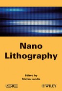
From a very simplistic point of view, the fabrication of integrated circuits concatenates and alternates two types of processing on the wafer (Figure I.1); either:
– a functional layer is deposited by a lithographic process. The material is localized by removing the extra material in the non-selected areas (subtractive process): this is the case, for example, for contact holes through an isolating layer; or
– a specific area is defined where a technological process is locally applied, the confinement system being removed at the end of the step (additive process): this is the case for ionic implantation or localized electro-deposition.
The efficiency of the lithographic process depends on only a few fundamental parameters:
– the capability of printing even the smallest patterns, or resolution;
– the precise alignment of each layer of a circuit;
– the capacity to obtain repeatable patterns, of a controlled geometrical shape;
– the capacity to control fabrication costs as a function of the products’ typology.
A greater integration density implies that the very smallest patterns must be able to be manufactured, hence the focus on ultimate resolution for lithography techniques. Patterns of just a dozen nanometers do not surprise anyone anymore, and even atomic resolutions are now achievable, with today's more sophisticated experimental conditions.
Optical lithography remains the preferred production choice. Despite inevitably being abandoned once the physical limits of the micron, and then of the 100 nm, are crossed, it remains today the preferred technique for mass production for 32 nm, thanks to the numerous innovations of the past 20 years.
In optical lithography, a polymer layer called a photosensitive resist is deposited on a wafer. This resist is composed of a matrix which is transparent to the exposure wavelength and contains photosensitive compounds. When the image of the patterns from a mask is projected onto the wafer (and onto the photosensitive resist), the areas exposed are submitted to a photochemical reaction which, if completed correctly, enables the dissolution of the resist in those areas (in the case of positive resists), or prevents dissolution (in the case of negative resists). We can therefore obtain perfectly delimited areas for which the substrate is bare, and have areas still protected by the resist, allowing a subsequent local treatment. At the end of the process, the resist is removed from the wafer. During the fabrication of integrated circuits, this step is repeated several dozen times, hence the central role of lithography in microelectronics.
Figure I.1. A localized process using lithography can be (a) subtractive (by locally removing non-functional material), or (b) additive (by forcing the local treatment of the wafer where it is required)
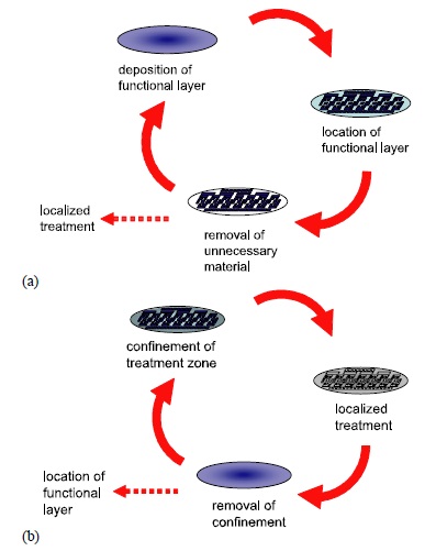
In order to understand simply how this technique reaches its highest resolution, we can refer to the standard formula giving the resolution, R:
in which λ is the wavelength of the exposure light, NA the numerical aperture of the projection optics and k1 a factor depending on the technological process. Each of these factors corresponds to a way of improving the image resolution.
Improvements were first made by decreasing the exposure wavelength λ. This was why, in the 1980s, the first tools started using different radiations from a mercury lamp (λ = 436 nm, called g-line radiation; 405 nm, or h-line; and then 365 nm, or i-line), usually using reduction projection optics based on quartz. Each wavelength change was accompanied by process changes that were major at the time, but which, in retrospect, could now be qualified as minor.
The first transition came in the 1990s with the use of deep ultraviolet excimer lasers, first with 248 nm (with a KrF laser) and then 193 nm (with an ArF laser), and allowed feature size resolution below the 0.1 µm limit to be reached. However, this evolution required major changes in either projection optics (use of CaF2 in addition to quartz) or in the choice of the transparent matrix of the photosensitive resist.
The normal evolution would have moved towards F2 lasers (λ = 157 nm) which need projection optics made mainly out of CaF2, a material whose bi-refringence has proven to be a major obstacle: in the decade after 2000, after many years of development, industry finally concluded that it was illusory to continue down this path for mass production.
Reducing the k1 parameter then appeared very promising. This is achieved by first improving the resist process, for example by increasing its contrast with nonlinear phenomena or by controlling the diffusion of the photosensitive compound. By optimizing illumination techniques (annular, quadripolar, etc.), it is also possible to gain resolution and process control but often by promoting certain shapes or pattern orientations.
It has been, above all, by mastering diffraction phenomena, and thus influencing the exposure light phases, that progress has been the most spectacular: it has been acknowledged that it is now possible to go beyond the Rayleigh criterion and print patterns even smaller than the exposure wavelength. From laboratory curiosities, these techniques have now become the workhorse of the microelectronics industry and are now known under the name “Resolution Enhancement Techniques”.
In a very schematic manner, and for a certain illumination and resist process, we will try to calculate what the patterns and phase-differentiated areas on a mask should be in order to achieve an image on a wafer which matches an image initially conceived by circuit designers. The reverse calculations are extremely complex and demand very powerful computers in order to obtain the result (in some cases taking up to several days, which affects the cycle time of prototypes of new circuits). In the end, the goal is to take proximity effects between close patterns (thus a combinational explosion of the calculation time) into account, by in turn taking into account the most precise possible optical models (and, as the technologies improve, it is important to not only take into account intensity and phase but also light polarization). The resulting pattern on a mask becomes particularly complex, and the cost of a mask set for a new circuit can exceed several million dollars for the most advanced technologies, which can become a major obstacle for small production volumes.
Despite this complexity, it is increasingly difficult to find a solution for arbitrary patterns (called random logic patterns, even though this term is inappropriate). The idea arose to simplify the problem by grouping patterns with the most periodicities (and therefore easier to process) and obtain the desired design on a wafer by multiple exposures. This approach, despite its significant production costs, has become common in the most advanced technologies.
Additionally, the numerical aperture (NA) of the projection tool has been studied, even though we know that an increase of the NA can only be made to the detriment of the depth of field. Of course, NA has increased over recent years, thus decreasing the size of the exposed field. This is why print patterns were “photo-repeated” by repeating the exposure of a field a few centimeters in size over the entire wafer (the tool used is called a photo-repeater or “stepper”), then the area exposed was reduced a little more by scanning a light-slit over the exposure field (using a tool called a “scanner”). Unfortunately lithography was limited by the numerical aperture, which could not exceed 1.
Researchers then returned to their old optical knowledge: by adding a layer of liquid (with a higher index than air) between the first lens of the exposure tool and the resist, the limit could be overrun. This “immersion lithography” has not been established without difficulties. The defect density generated by this process was at first high, not to mention there being an increased complexity of the lithographic tool. The conjunction of these major difficulties encountered in 157 nm lithography and the need to decrease the dimensions made this technique viable and it is starting to be used for mass production.
The next step was to increase the refraction index of the liquid to above that of water, and that of the projection systems (the lenses) to above that of quartz. However, in the case of 157 nm, this approach is blocked by major material problems, and the future of this path beyond that of the resist-water-quartz system seems highly endangered.
Many believe that a major decrease of the exposure wavelength would significantly relax the constraints that apply to lithography. Hence there has been a unique worldwide effort to develop Extreme UltraViolet lithography (EUV) using the 13.5 nm wavelength. However, despite an enormous effort during the past two decades, this technology stays blocked by major problems of source power and industrial facilities able to produce defectless masks. Initially foreseen to be introduced for 90 nm technologies, it has difficulties addressing 22 nm technologies. As a result, initially peripheral aspects, such as high numerical aperture optics, come back to the forefront, even though other technological problems are still unresolved for industrial manufacturing.
Complexity has considerably increased the cost of lithography for the fabrication of integrated circuits for the most advanced technologies. The newest immersion scanners, in addition to their environment (resist coating track, metrology) easily cost over $50 million each, and it would not be surprising if a price of $100 million was reached with EUV, hence the large amount of research into alternative technologies to optical lithography in order to either significantly decrease the cost or to address very specific applications that do not necessarily need the most advanced lithographic tools.
One alternative technique was established a long time ago: electron beam (often called “e-beam”) lithography. This technique is not limited by wavelength or by depth of field, thus making it very attractive. The absence of a mask is an additional advantage when looking at the never ending increase of mask prices, especially in the case of small volume production. The disadvantage of this technique is that pattern printing can only be achieved sequentially (the electron beam writes in the resist pixel after pixel), which does not allow high enough productivity for mass production. In addition, e-beam can no longer claim its superiority in terms of resolution and alignment precision because of the continuous progress of optical lithography. However, new projects are being developed, among which is the idea of massively multiplying the number of independently controlled beams (tens of thousands of beams is the number stated): productivity would then increase significantly, with the prospect of it being applied to small volume production. In addition to this application, electron beam lithography remains a preferred tool for research activities that can combine flexibility, dimension control and affordable price. It can also be used to precisely repair circuits (or to print specific patterns on demand), using either an electron or an ion beam.
Other alternative techniques offer interesting prospects for precise applications:
– NanoImprint lithography, similar to the techniques used to fabricate CDs or DVDs from a master. This enables nanoscale resolutions to be achieved, and could emerge as a contender technology if there were only one lithographic level. It has also been shown that this technique could be used to print 3D patterns. The stacking of dozens of layers in integrated circuits is still to be demonstrated industrially, in particular in terms of alignment precision and defect density due to fabrication.
– Near-field lithography is still the perfect tool when aiming for ultimate resolution (potentially positioning atoms one by one). Its current state suffers from the same intrinsic limitations as electronic lithography (small productivity) as well as a difficult setting when reaching ultimate resolutions, but this technique could open up to real prospects with tip-matrices of the millipede type.
– X-ray lithography was, for a long period after the major efforts of the 1980s, not considered adequate to become an industrial technique. Source weakness (even if synchrotrons are huge experimental systems), the difficulty of fabrication of transparent masks and the absence of reduction optics have heavily handicapped the future of this technique. However, it remains useful for specific applications (such as the LIGA technique1) given its great field depth that can be used in microsystems.
A special note should be made about self-organizing techniques. These rely on a simple fact: nature seems to be able to generate complex structures from apparently simple reactions. More specifically, local interactions can induce unexpected or even complex, emerging behaviors: this is called self-organization. Convincing examples of periodic structures generated by these techniques are regularly submitted to the scientific literature; however, it is hard to find an idea to exploit this technique in order to produce future low cost microprocessors. Thus, two directions now exist:
– the use of these phenomena to locally improve process quality. For example, the use of resists based on copolymers could help improve the line roughness of lithographic patterns; and
– the notion of “directed self-assembly” or “emplated self-assembly”, which is the most important direction for more complex structures. This is about defining and implementing limit conditions that, using local self-organization forces, could generate the complex structures desired.
Finally, it is important to remember that the fabrication cost aspect of these emerging technologies remains completely speculative, since the technical solutions to be implemented on an industrial scale are still unknown.
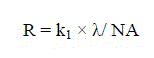
This focus on ultimate resolution as the connecting thread of this book should not hide other technical elements that are also critical for lithography's success. Thus, popular literature often forgets that the capacity to stack two patterns greatly contributes to the capacity to integrate many compounds in a circuit. Indeed if patterns are misaligned, an area around the pattern would have to be freed to ensure the functionality of the circuit, thus reducing the integration density (Figure I.2). Achieving alignment with a precision equal to a fraction of the minimum size of the pattern (a few nm), and measuring it, represents a challenge that lithography has so far been able to meet.
Figure I.2. The precise alignment of patterns printed at different lithographic levels influences the compound integration density of a circuit. For example, in the case of the command electrode of a transistor: (a) with significant misalignment, the command electrode of a transistor could possibly no longer control the active zone of the compound. (b) In order to avoid this situation, the electrode's size is increased. As a result, those electrodes which are close must be moved, thus inducing a degradation of the integration density
The functionality of a circuit will depend on the precision at which the patterns on the wafer are printed. Metrology is a key element in mastering the production yield, whereas the demands regarding precision, information integrity and measurement speed keep growing. Previously, optical microscopy techniques were enough to measure, in a relative way, the two critical parameters of a lithographic step, meaning the dimension of its pattern and alignment in relation to the underlying layers. As dimensions have decreased, standard optical techniques were replaced by different approaches:
– the use of an electron beam microscope (and more recently near-field techniques) enabled a natural extension to the smallest dimensions;
– light scattering of periodic patterns (for example scatterometry) gave access to more complete information on the dimensions and shape of the patterns, even though the interpretation of the results remains unsure. A move towards shorter wavelengths (for example SAXS for X-rays) opens up new perspectives (as well as some advantages, for example with substrate transparency).
However, the challenges to be fulfilled keep increasing. A relative measurement is no longer sufficient to guarantee a circuit's performance and the possibility of an absolute metrology on a nanometric scale still remains. In addition, the shape of the pattern is increasingly a 3D measurement which is essential, at least when considering mass production, even if the techniques used are still in the embryonic stages. Finally, the proximity effects between patterns make the measurement indicators less representative of the complexity of a circuit: the metrology of a statistical collection of meaningful objects in a complex circuit is a field of research that is still wide open.
It is important to mention a technical field which, even if not part of lithography in the strictest sense, is to a large extent connected to it: the measurement of physical defects in a production process. Indeed, two different aspects of the analysis and measurement of defectivity are interesting:
– For defects with an identified physical signature, techniques similar to lithography can be applied because it concerns acquiring an image with optical techniques (in the broad meaning, including charged particle beams) and treating it in order to extract meaningful information.
– Lithography is unique in the way that, in the case of the detection of a defect during this step, it is usually possible to rework the wafer and thus avoid the permanent etching of the defect into the circuit.
In conclusion, lithography has undergone several decades of unimaginable progress, by-passing unproven physical limits thanks to the ingenuity of microelectronics researchers and engineers. Even if questions emerge about the economic viability of dimension decrease at all costs, major steps forward are expected during the coming years, either in terms of the solutions reached, the integration density or capacity to produce cheap complex structures.
1 Introduction written by Michel BRILLOUËT.
1 LIGA is a German acronym for Lithographie, Galvanoformung, Abformung (Lithography, Electroplating, Molding).