
6
Big Data Search Engines and Deep Computers
6.1 Overview of Big Data Search Engines and Deep Computers
The Internet of Things (IoT) collects a large amount of data, much of which is stored in large server farms called collectively “The Cloud”. These data are only useful if they can be accessed intelligently and efficiently. An example of a basic data search engine is a ternary content addressable memory (TCAM). This is a memory that can compare input search data with stored data and return the location of matched data. TCAMs are used in both MPU designs and in communication chips such as those for IP‐routing.
Deep computers and artificial intelligence will also be needed to intelligently process the data in The Cloud. In addition to neuromorphic computers, which were discussed in an earlier chapter, extreme learning machine architectures and artificial intelligence are being developed. Deep learning can be implemented using a restricted Boltzman machine, which consists of a generative stochastic artificial neural network. Deep learning involves extracting complex information from high‐dimensional data without using significant amounts of manual engineering. It is useful for image recognition, speech recognition, and natural language understanding.
6.2 Content Addressable Memories Made Using Various Emerging Nonvolatile Memories
A content addressable memory, or associative memory, searches its entire contents in a single clock cycle. It is commonly used for high speed search applications. A ternary CAM (TCAM) can store and query data using three different inputs 0, 1, and an extra input, which allows the TCAM to perform broader searches based on pattern matching.
Historically TCAMs have been implemented using static RAMs. In advanced technologies, the subthreshold leakage of SRAMs result in high power consumption. Several of the emerging memories, such as MTJ MRAMs, FeFETS, and RRAMs, have ultralow standby power and can also be used to make area and power efficient search engines and TCAMS. Each, however, has different trade‐offs in other characteristics.
6.2.1 Ternary CAMs Using Resistive RAMS
RRAMs can be used in TCAM for big data processing to replace SRAMs. A conventional TCAM cell uses 16 transistors. In 2014, NTHU, NCTU, NDL, and ITRI proposed an RC‐filtered stress‐decoupled four‐transistor and two‐resistor (4T2R) nonvolatile TCAM [1]. The device could be used to suppress match‐line leakage current from match cells, to reduce parasitic load, and to decouple nonvolatile memory (NVM) stress from word length A 128 × 32 nonvolatile TCAM (nvTCAM) macro was made using an HfO2‐based RRAM in 180 nm CMOS technology. In 2015, a 3T1R nvTCAM, which used a multilevel cell (MLC) RRAM was discussed by NTHU, ITRI, and NCTU. The device had a less than 1 ns search delay (Tsd) [2]. A conventional 16 T SRAM TCAM cell is shown in Figure 6.1 (a) and the 3T1R RRAM TCAM cell using an MLC RRAM is shown in (b).

Figure 6.1 TCAM cells: (a) 16‐transistor SRAM cell plus NVM and (b) bidirectional voltage divider control for a 3T1R nonvolatile TCAM using MLC RRAM.
Based on L. Huang et al. (NTHU, NCTU, NDL, ITRI), VLSI Circuit Symposium, June 2014 [1].
The 2 × 64 × 64b 3T1R nvTCAM macro was made using a back‐end‐of‐the‐line (BEOL) fast write HfO2‐based RRAM added to a 90 nm CMOS logic process. This device had a 2.27 times cell size reduction compared with SRAM TCAM in the same technology. The challenges of building this nvTCAM included: area and wire routing for the BEOL RRAM, the need for a higher write current for a long data retention time, and the large resistance ratio, which resulted in a large NVM driver area.
A register‐based timing extraction method was used to derive Tsd from the test chip search time by excluding the path delay time of the test chip as well as the load board. The measured worst case Tsd of a 3T1R nvTCAM macro at minimal VDD of 1 V is 0.96 ns. The nvTCAM search engine is shown in Figure 6.2.
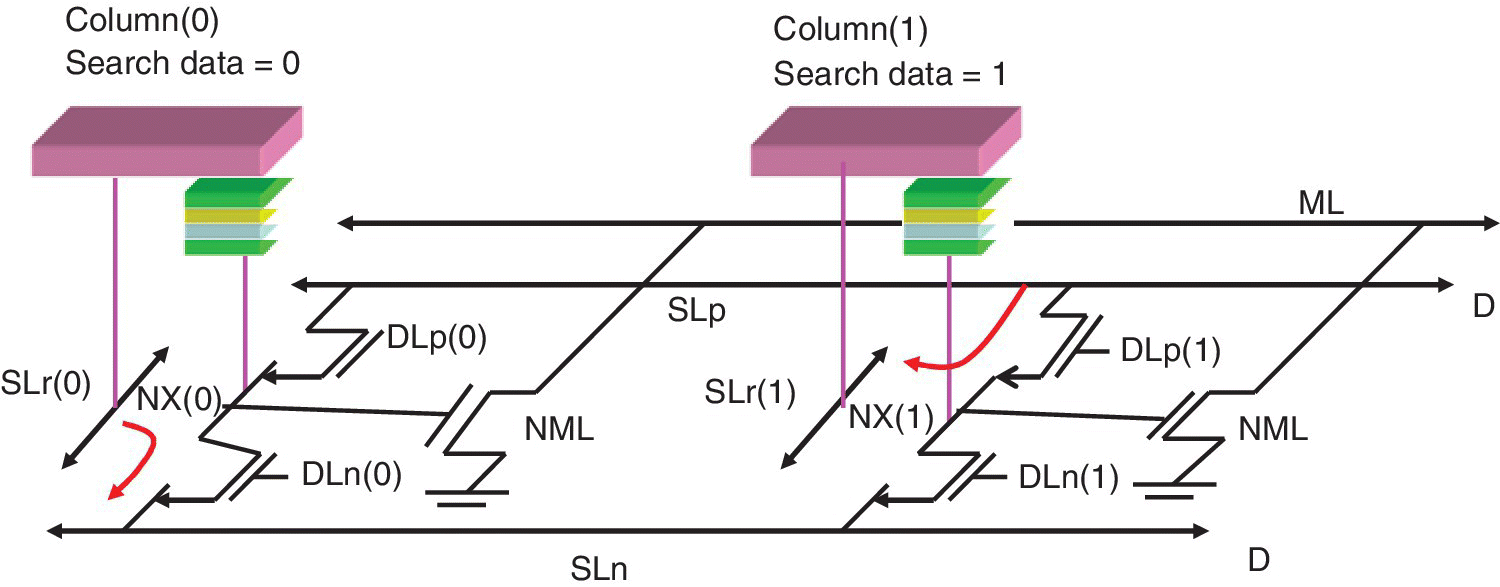
Figure 6.2 Circuit diagram of nvTCAM search engine using RRAM for data storage.
Based on M.‐F. Chang et al. (NTHU, ITRU, NCTU), ISSCC, March 2015 [2].
The larger current ratio and minimal number of devices stacked between power rails enabled operation at a low 0.48 V VDD with Tsd = 11.3 ns. The RRAM write speed for SET and RESET was less than 5 ns. Memory capacity was 2 blocks × 64 rows × 64 bits. Cell size was 0.8704 µm2. Search speed was 0.96 ns at VDD = 1 V at 25 °C. Vddmin was 0.48 V at 25 °C. Supply voltage was 0.5–1 V for search and 1.8 V for write.
A nonvolatile ternary content addressable memory (nvTCAM), which was used in network and big data processing, was discussed in 2016 by NTJU, TSMC, and NCTU [3]. The 256 bit wordlength nvCAM was based on an RRAM and was designed to reduce the cell area, search energy, and standby power over that of a SRAM‐based TCAM. These advantages were particularly expected in applications with long idle times and frequent‐search‐few‐write operations. A small 2.5 transistor and 1 resistive RAM (2.5T1R) cell was made in a 65 nm CMOS logic process. This cell reduced area and metal line capacitance. A 64 × 256 bit 2.5T1R nvTCAM macro was made using the 2.5T1R cell and the TSMC logic‐process‐contact‐RRAM. A DFF‐based timing extraction method was used to derive Tsd by excluding the path delay of the PCB. The measured worst case Tsd (1b mismatch time) with Vdd = 1 V was 1 ns.
6.2.2 CAMs Made Using Magnetic Memory
In February of 2015, Aligarh Muslim University discussed a TCAM made with a five‐layer MTJ configuration called a “PentaMTJ” [4]. The structure of the perpendicular magnetic anisotropy (PMA)‐based fivelayer TCAM MTJ is shown in Figure 6.3. It is composed of two pinned layers, one free layer, and the three metallic contacts.
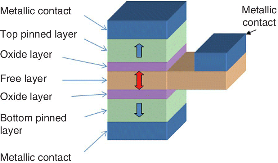
Figure 6.3 Perpendicular magnetic anisotropy (PMA)‐based five‐layer TCAM MTJ with two pinned layers and one free layer.
Based on M. Gupta and M. Hasan (Aligarh Muslim University), IEEE Trans. on Magnetics, February 2015 [4].
It is known that PMA is responsible for a lower threshold current due to the absence of the easy‐plane anisotropy term. This TCAM MTJ gives guaranteed disturbance‐free read since the net torque acting during sensing always acts to retain the previous state and increases the tolerance to process variations due to its differential nature. A block diagram of a TCAM using the “PentaMTJ” cell is shown in Figure 6.4. This architecture is made up of three parts: a pre‐charge sense amplifier (PCSA) for sensing the difference between two states of resistance, a logic circuit, and a TCAM writing cell with reference resistance.

Figure 6.4 Block diagram of TCAM using PentaMTJ cell, a pre‐charge sense amplifier (PCSA) for sensing the difference between two states of resistance, a reference resistance, and a logic circuit.
Based on M. Gupta and M. Hasan (Aligarh Muslim University), IEEE Trans. on Magnetics, February 2015 [4].
Using the PentaMTJ cell in the TCAM instead of a conventional MTJ provides a cell that is less affected by process variation. The pair of PentaMTJ cells increases the sense margin and robustness. This TCAM has low power consumption compared with existing MTJ‐based CAMs since it uses a pre‐charge sense amplifier (PCSA) for sensing. It is immune to masking error since the masking is done by putting the transistor in the OFF state rather than by storing the same data in the two MTJs.
A spin memory device that could be used for matching and self‐reference function in a non‐volatile content addressable memory (CAM) was discussed by Avalanche Technology in November of 2015 [5]. This spintronic memory used a spin–torque interaction combined with conventional spin–torque generated by magnetization polarization. The nvCAM macro was used along with a DRAM macro on a chip for data intensive computing applications such as data mining, search engines, scientific computing, and video processing. A block schematic of the spin CAM chip architecture is shown in Figure 6.5. This spin memory device had matching and self‐reference functionality for use in content addressable applications. It included a spin content addressable memory (CAM) structure consisting of a DRAM cell with an embedded dual spin hall MTJ CAM device. This study investigated how to implement a spintronic memory computing device for parallel match‐in‐space and content addressable applications using SOT MRAM. A spin orbit CAM device and circuits were proposed that are capable of multibit match‐in‐space functionality and single bit nondestructive self‐reference functionality.
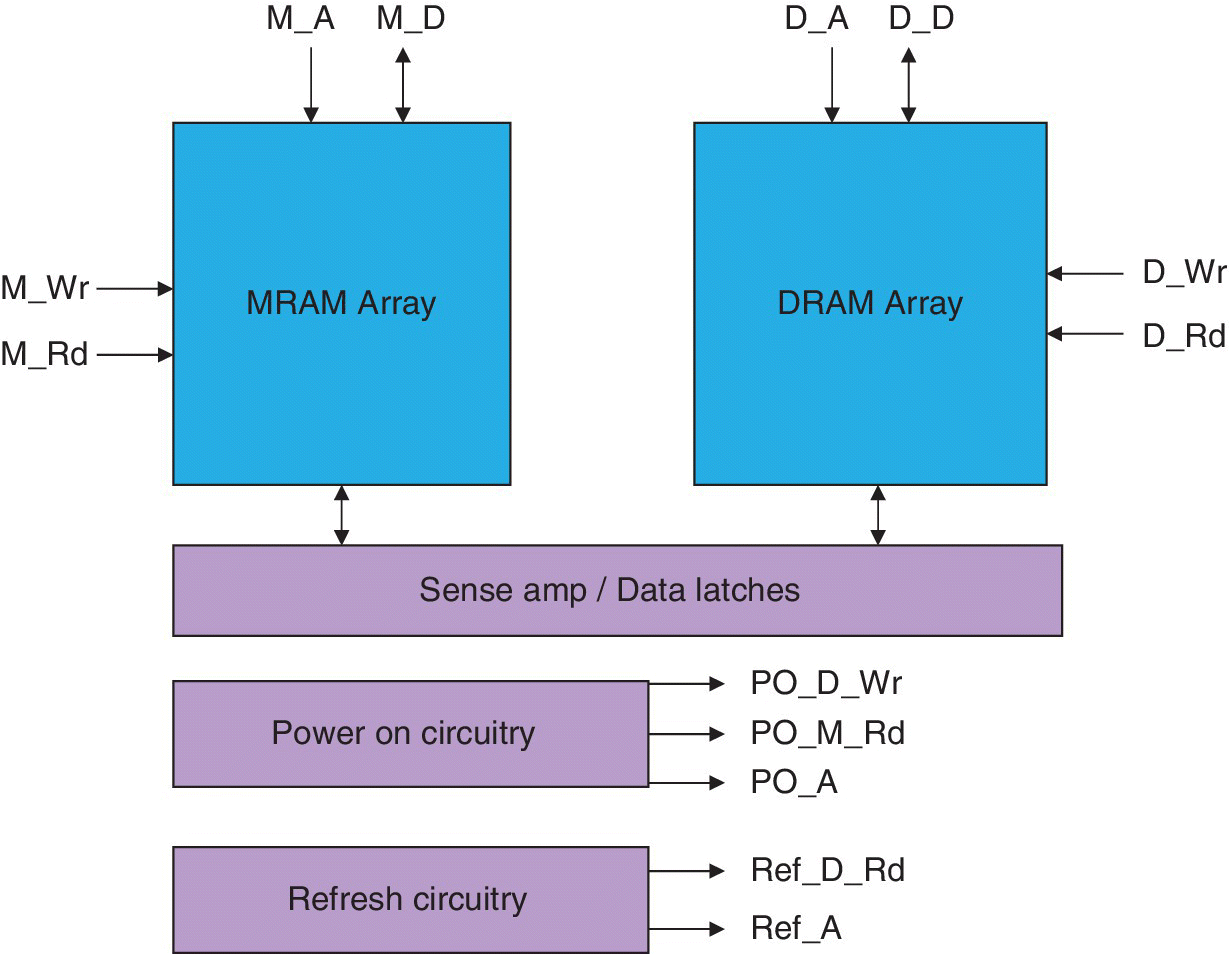
Figure 6.5 Block schematic of spin CAM architecture of a DRAM cell with embedded MRAM.
Based on X. Wang et al. (Avalanche Technology), IEEE Trans. on Magnetics, November 2015 [5].
A low power, compact, and massive parallel comparison is provided by this spin‐orbit memory device. The power consumption could be significantly reduced due to reduced leakage current over that of an SRAM CAM and the massive parallel array could increase system operating speed significantly.
The spin CAM architecture proposed combined DRAM with embedded MRAM. In this architecture of DRAM with embedded MRAM, the DRAM is used to reduce the cell size, while the MRAM is used to store bit content and to refresh the DRAM. During device operation, there is no need to explicitly read on‐chip DRAM. DRAM external refresh will not interrupt normal operations. A circuit with an MRAM refreshing DRAM is shown in Figure 6.6.
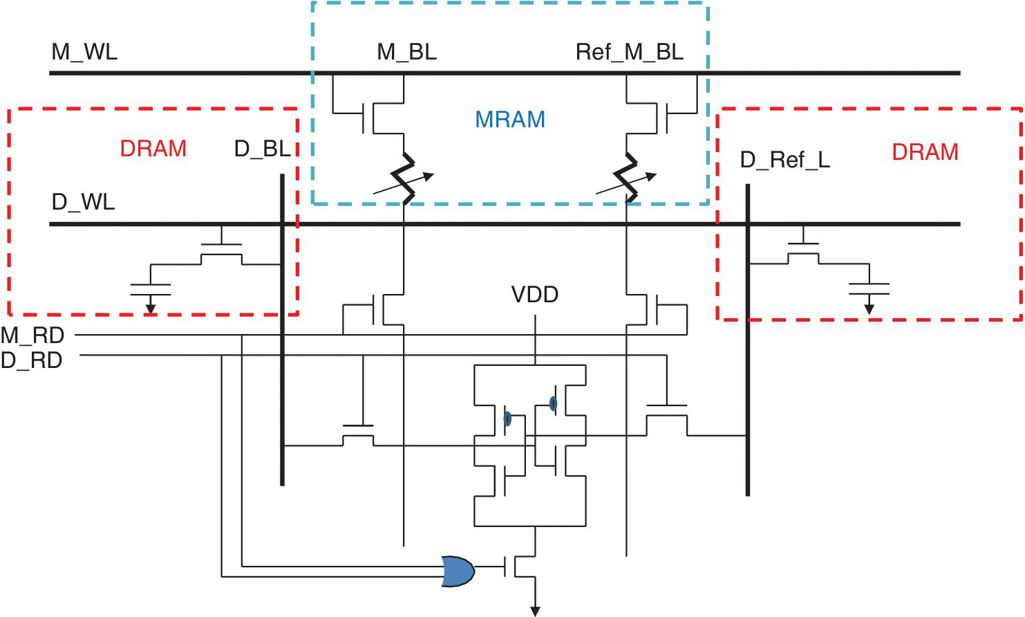
Figure 6.6 Schematic CAM circuit showing an MRAM refreshing DRAM circuit.
Based on X. Wang et al. (Avalanche Technology), IEEE Trans. on Magnetics, November 2015 [5].
A multibit parallel match‐in‐space array circuit structure using a multibit marching and single bit self‐reference device was also discussed. This circuit used a spin hall metal layer. It had two writing current paths, the first to switch the free layer magnetization using spin torque, while the second current path switched the comparison reference layer magnetization through the spin torque generated by spin–orbit interactions. Two separated write paths are able to independently switch the magnetization of either the free layer or the comparison reference layer.
The main benefits of the spin–orbit memory device are low power, compact area, and massive parallel comparison. The 1T1R spin–orbit CAM structure reduces the cell area and the massive parallel comparison array increases the system operating speed.
6.2.3 CAMs Using Other Emerging Memories
The TCAM is a special type of memory that can compare input search data with stored data and retrieve the matched data. In August of 2014, the University of Pittsburgh discussed TCAMs made of various eNVM technologies [6]. These technologies included tunneling junction (MTJ), resistive RAMs, and ferroelectric FET. It was found that all three types of emerging memories could achieve nearly zero standby power.
6.3 Components of Large Search Engines and Artificial Neural Networks
6.3.1 Using RRAMs in Look‐Up Tables in Large Search Engines
Look‐up tables (LUT) are necessary in large search engines. In November of 2014, ITRI, National Taipei University, NTHU, and Min Shin University discussed a nonvolatile look‐up table that used RRAM for the reconfigurable logic [7]. The circuit used RRAM cells with normally off and instant‐on functions for suppressing standby current. The proposed RRAM‐based two‐input nonvolatile look‐up table (nvLUT) circuit decreased the number of transistors by 79% and the area of the nvLUT by 90.4% compared with the area of a SRAM‐MRAM hybrid LUT. The areas of two‐input RRAM nvLUTs were found to be smaller than MRAM‐based two‐input nvLUTs. Due to low current switching and high resistance ratios, the RRAM‐based nvLUT had 24% less power consumption than SRAM‐MRAM hybrid LUTs. Functionality of the adder of the three‐input RRAM nvLUT was confirmed using an HfOx‐based RRAM made in 180 nm CMOS logic with a 900 ps delay time.
A TiN/TiOx/HfOx/TiN stack was used for the RRAM. SET operation, which is the low resistance state, used a positive 1.5 V and RESET, which is the high resistance state, used a negative one (–1.1 V). Write time of the HfOx‐based RRAM was as fast as 5 ns. The architecture of the proposed 1T2R memory unit is shown in Figure 6.7. It consisted of an NMOS select transistor and two HfOx RRAMs. The RRAM devices RA and RB work together as a complementary resistive switching (CRS) device.

Figure 6.7 Circuit schematic of the 1T2R memory unit with 1T and 2RRAMs which act as a complementary resistive switching (CRS) device.
Based on W.‐P. Lin (ITRI, National Taipei University, NTHU, Min Shin University), IEEE A‐SSCC, November 2014 [7].
A resistive RAM crossbar array can be used for matrix vector multiplication. In 2015, Tsinghua University and Arizona State University discussed using an HfOx RRAM crossbar array for matrix‐vector multiplication [8]. If a 2D filament model of the HfOx‐based RRAM is considered, the conductance is exponentially dependent on the tunneling gap distance d, as illustrated in Figure 6.8.

Figure 6.8 Schematic cross‐section of 2D filament model of HfOx‐based RRAM.
Based on P. Gu et al. (Tsinghua University, Arizona State University), ASP‐DAC, January 2015 [8].
When a large voltage is applied on the electrodes, d will change due to the electric field and temperature‐enhanced oxygen ion migration. The resistivity of the RRAM will switch between the highest resistance state Roff and the lowest resistance state Ron. In theory an RRAM can achieve any resistance between Ron and Roff. This study discussed choosing the resistivity of the RRAM device.
The I–V relationship can be expressed as

where d is the average tunnel gap distance and I0 and V0 are determined experimentally.
The RRAM crossbar array can perform analog matrix vector multiplication. The relationship between the input voltage and the output voltage vector can be expressed as
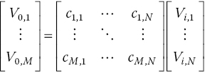
The matrix parameter Ck,j can be represented by the conductivity of the RRAM device and the load resistor as
For a more linear I–V relationship for the RRAM device, both the RRAM resistance state, represented by the tunneling gap distance d and the applied voltage V, should be confined.
Hybrid RRAM and triple level cell (TLC) NAND Flash can be used for data storage in RAID servers in large server farms. In February of 2014, Chuo University and the University of Tokyo discussed hybrid storage of RRAM and three‐level cell (TLC) NAND Flash with RAID‐5/6 [9]. RAID‐5/6 is commonly used in Cloud storage and data warehouses due to having a lower parity overhead than RAID‐1. The proposed architecture gave significant improvements in reliability and performance of RRAM and TLC NAND. Data to RRAM was encoded and then written to RRAM.
RRAM crossbar arrays can be used in large memory systems as a potential scaling replacement for DRAM. In February of 2015, the Oakridge National Labs discussed RRAM for its superior characteristics such as high density, low write energy, and high endurance [10]. This study did a comprehensive review of RRAM memory systems using stacked crossbar architecture with peripheral circuits below the multiple layers of RRAM cells. The crossbar architecture was found to have constraints on operating voltages, write latency and array size.
Architectural optimizations were obtained from the relationship between the RRAM write voltage and switching latency. Trade‐offs involving voltage drop, write latency, and data pattern were discussed and microarchitectural enhancements were analyzed, including double‐sided ground biasing and multiphase RESET operations to improve write performance. A simple compression‐based data encoding method was used to reduce the latency. Since the compressibility of a block varies based on its content, write latency is not uniform across blocks. To reduce the impact of slow writes on performance, a new scheduling policy was explored that made writing decisions based on latency and activity of a bank. Experimental results showed that the stacked crossbar architecture improved the performance of a system with RRAM main memory by about 44% over a baseline DRAM system.
6.3.2 Using STT MRAM in Large Artificial Neural Networks
STT‐MRAM acting as a stochastic memristive device was discussed in 2014 by the University of Paris‐Sud, CNRS, CEA, and LIST [11]. The device was used to implement a “synaptic” function. Basic concepts of STT‐MRAM cell behavior were considered for the potential of implementing synapses capable of learning. A simulation of the synapse was used on an application of “car counting” to show the potential of the technology. A Monte Carlo simulation was used to show the robustness of the technology to device variations.
The ability of a positive current to switch the MTJ in one direction and a negative current to switch it in the opposite direction was taken as similar to a binary bipolar memristor. Using usual mathematical descriptions of an STT‐MTJ MRAM, an expression similar to a memristor was derived. An STT‐MRAM synapse and a leaky integrate and fire (LIF) neuron learning system is shown in Figure 6.9.
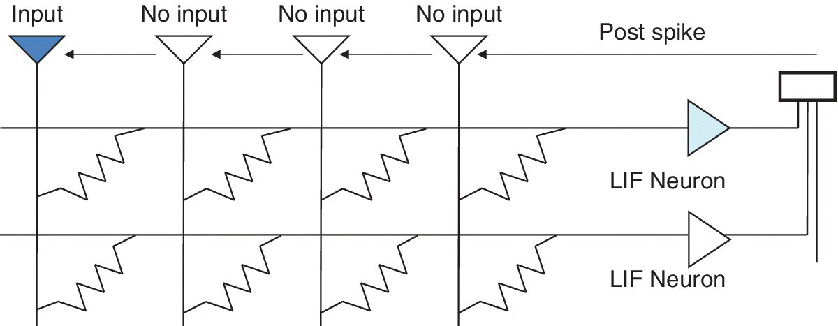
Figure 6.9 Schematic circuit diagram of crossbar architecture for learning system using STT‐MRAM synapses and leaky integrate and fire (LIF) neurons.
Based on A.F. Vincent et al. (University of Paris‐Sud, CNRS, CEA, LIST), ISCAS, June 2014 [11].
System level simulation of stochastic MTJ synapses were shown using a method previously proposed for conductive bridge RAM. In this system, input neurons present short low voltage spikes that generate current through the crossbar. The conductance of the MTJ acted as a synaptic weight converting voltage into current. The current was integrated by output neurons until one of them generated a spike, which then inhibited the other output neurons.
In April of 2015, the University of Paris‐Sud, CEA, and Beihang University discussed further on an STT MRAM used as a stochastic memristive synapse [12]. The STT‐MTJ MRAM was used for implementing learning capable synapses. Low, intermediate and high current programming regimes were identified and compared.
An example of the function for system‐level simulations for a vehicle counting application showed the potential of using the technology for learning systems. Monte Carlo simulations were done to show robustness to device variations. The simulations also compared system operation with different programming regimes of the STT‐MTJs. The intermediate current regime was compared to the high and low current regimes and was shown to permit minimization of energy consumption while retaining robustness to device variations. The conclusion was that applications using STT‐MTJ as synapses in robust, low power, cognitive systems were possible.
Artificial neural networks (ANNs) using spin synapses and neurons were discussed in 2016 by Beihang University, the University of Paris‐Sud, and Tsinghua University [13]. Spintronic devices using MTJ as a binary device have been explored previously for neuromorphic computing with low power dissipation. This study used a compound spintronic device consisting of multiple vertically stacked MTJs, which behaved as a synaptic device.
It was shown that the compound spintronic device could achieve designable and stable multiple resistance states for use as synapses by doing interfacial and materials engineering of its components. A compound spintronic neuron circuit was developed based on a spintronic device that enabled a multistep transfer function. An artificial neural network was constructed using both the spin synaptic and spin neuron circuits. A test of the NMIST database for handwritten digital recognition was done to evaluate the performance of the ANN. The MNIST database was constructed from NIST databases that contained binary images of handwritten digits.
A schematic of the proposed compound spintronic device is shown in Figure 6.10. The capping layer materials and thickness and MgO tunneling barrier thickness can be manipulated separately to get designed multilevel states. Ideally, N vertically stacked MTJs can exhibit 2 N states. It was demonstrated that four distinct states could be obtained; then it was inferred that by vertical stacking more MTJs more resistance states could be achieved. Ideally, 2 N resistance states can be achieved by stacking N MTJs.
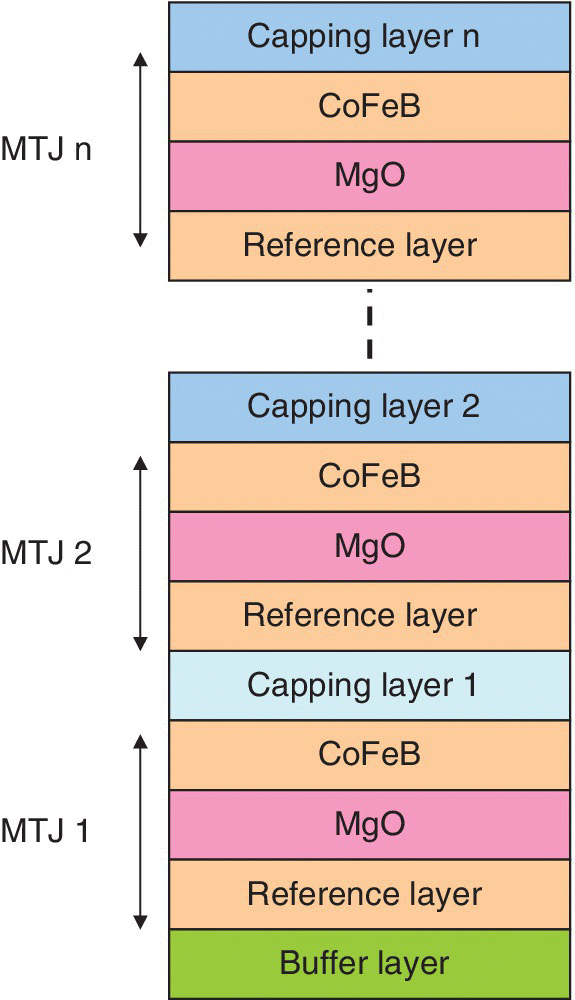
Figure 6.10 Schematic of the compound spintronic device showing “n” multilevel states.
Based on D. Zhang et al. (Beihang University, University of Paris‐Sud, Tsinghua University), IEEE Trans. on Biomedical Circuits and Systems, August 2016 [13].
A neuron is the basic computational element in an ANN. It generates an output signal depending on the magnitude of the summation of its synaptic weighted input signals. The neuron’s output signal is then transmitted by way of the axon as the input of its fan‐out neurons. A single MTJ device has been shown to be able to emulate the step transfer function, which corresponds to the switching between its two stable states by a resultant synaptic current in ANNs. For a nonstep transfer function, a compound spintronic neuron that also uses multiple MTJs can function as a single neuron. Figure 6.11 shows a proposed compound spintronic neuron intended to implement a multiple step transfer function.

Figure 6.11 Illustration of a compound spintronic neuron using multiple MTJs to implement a multiple step transfer function.
Based on D. Zhang et al. (Beihang University, University of Paris‐Sud, Tsinghua University), IEEE Trans. on Biomedical Circuits and Systems, August 2016 [13].
The performance of the artificial neural network was studied by performing system‐level simulations with off‐line training on the NMIST database for handwritten digital recognition. It was shown that the proposed compound spintronic synapse (CSS) and compound spintronic neuron (CSN) could be used to build a next‐generation neural computation platform.
6.4 Memory Issues in Deep Learning Systems
6.4.1 Issues with Partitioning SRAM and RRAM Synaptic Arrays
Memory arrays are being used for on‐chip acceleration of weighted sum and update in neuromorphic machine learning. Since the learning algorithms operate on a large weight matrix size, an efficient mapping of the matrix may require partitioning it into a number of subarrays.
In May of 2016, Arizona State University discussed a circuit‐level macrosimulator intended to partition a 512 × 512 weight matrix into RAM‐based accelerators using both SRAM and RRAM [14]. For an SRAM, increased partitioning and finer granularity of the array leads to decreased read and write latency and decreased dynamic read and write energy. This is due to the increased parallelism obtained at the cost of larger area and leakage power. For an RRAM accelerator, however, increased partitioning increased the read latency and energy only to a certain partition point due to the overhead of multiple intermediate stages of adders and registers.
In the neural network, the weight is represented by a synapse element. The connections through synapses between neurons form a weight matrix. The key operations of learning algorithms are the weighted sum and weight update. Hardware acceleration of neurocomputing consists of efficiently mapping the learning algorithms on‐chip to improve computing speed and reduce power consumption. Early large neuromorphic hardware platforms have been based on CMOS SRAM‐based synaptic arrays. An SRAM accelerator is illustrated in Figure 6.12.
Figure 6.12 Block diagram of SRAM accelerator using CMOS SRAM‐based synaptic arrays.
Based on P. Chen and S. Yu (Arizona State University), ISCAS, May 2016 [14].
6 T SRAM cells are grouped as one weight element. The weighted sum (read) and weighted update (write) operations are performed on a row‐by‐row basis. The adder and resister are added to help accumulate the partial weighted sum of each row.
More recently, RRAM crossbar arrays have been used for weighted sum and update in learning algorithms. Since the RRAM can have multiple levels per bit it can be used for storing analog weights at a high density. Scaling up the array size is an issue and requires efficient partitioning.
An RRAM accelerator with a pseudo‐crossbar array core (with the crossbar array rotated 90 degrees) is shown in Figure 6.13.
Figure 6.13 RRAM accelerator with pseudo‐crossbar array core.
Based on P. Chen and S. Yu (Arizona State University), ISCAS, May 2016 [14].
The weight update (write) is through the BL and SL switch matrix with one row activated. Weighted sum operation (read) is through the BL switch matrix (input vector) with all rows activated. If a limited number of read circuits are shared, the weighted sum operation may need to be time‐multiplexed.
It was suggested that the large array can be partitioned into N × N small arrays in a hierarchical manner to speed up the write operation since the weight elements in different subarrays can be updated in parallel. For a read, the vector and matrix were distributed into the subarray partitions and computed in parallel. The results from all subarrays were collected and summed. Multistage adders and registers were used to get the final weighted sum. The resulting read and write latency per operation for the SRAM and RRAM accelerators with different numbers of partitions in a 256 kb (512 × 512) array are shown in Figure 6.14.
Figure 6.14 Illustration of read and write energy per operation for SRAM and RRAM.
Based on P. Chen and S. Yu (Arizona State University), ISCAS, May 2016 [14].
The improvement in read latency of the RRAM array is limited due to added adders and registers, which are included in the time‐multiplexing. The read and write energy consumption per operation for the SRAM and RRAM accelerators with different numbers of partitions in a 256 kb (512 × 512) array are shown in the figure. While the SRAM continued to improve in read energy consumption with an increased number of partitions, the RRAM array showed a minimum read energy consumption at about 8.8 partitions, which corresponds to an array size of 64 × 64. Both arrays continued to improve in write energy with increasing partitioning. The leakage power consumption of the RRAM accelerator was less than that of the SRAM at a small number of partitions, but increased with partitioning to nearly that of the SRAM accelerator at the (8 × 8) array size corresponding to 64 partitions.
6.4.2 Issues of RRAM Variability for Extreme Learning Machine Architectures
The intrinsic variability of filamentary resistive memory for extreme learning machine architectures was discussed in 2015 by the Indian Institute of Technology of New Delhi [15]. This paper showed the unavoidable device variability of RRAMs for designing efficient low power low footprint extreme learning machine (ELM) architectures. The system discussed used the uncontrollable off‐state resistance (Roff/HRS) spreads for several RRAM types, as illustrated in Figure 6.15.

Figure 6.15 Illustration of extracted HRS/Roff lognormal distributions for filamentary RRAM devices.
Based on M. Suri and V. Parmar (IIT New Delhi), IEEE Trans. on Nanotechnology, November 2015 [15].
The RRAM‐ELM architecture proposed was demonstrated in two applications, a diabetes diagnosis test and a SinC curve‐fitting regression. The ELM discussed was a single‐layer feed forward neural net consisting of: hidden layer synapses with randomly assigned weights, a hidden neuron layer with an infinitely differentiable activation function, and an output layer with synaptic weights determined by a learning rule. The training block architecture proposed is shown in Figure 6.16. It was shown that HRS distributions can be used for input‐stage random synaptic weights and random neuron biases.

Figure 6.16 Illustration of training block in RRAM extreme learning machine (ELM) architecture, where H is the hidden layer neuron output and T is the expected output. Both are stored inside the training block.
Based on M. Suri and V. Parmar (IIT New Delhi), IEEE Trans. on Nanotechnology, November 2015 [15] (permission of IEEE).
6.4.3 Issues with RRAM Memories in Restricted Boltzman Machines
Deep learning can be implemented using a restricted Boltzman machine (RBM), which consists of a generative stochastic artificial neural network capable of learning a probability distribution over its set of inputs. RBMs are typically used as building blocks for deep belief networks. In October of 2015, IEF‐CNRS and IEMN‐CNRS in France discussed the development of a hybrid RRAM‐CMOS RBM architecture in which HfO2‐based RRAM devices are used to implement synapses, internal neuron state storage, and stochastic neuron activation function [16]. The RBM architecture was simulated for classification and reconstruction of handwritten digits on a reduced MNIST data set of 6000 images. The required size of the RRAM matrix in the simulated application was on the order of 0.4 Mb. Peak classification accuracy was 92% and an average accuracy of 89% was obtained over 100 training periods. The average number of RRAM switching events was 14 million/period. The I–V characteristics of the OxRAM (oxide‐based RRAM) device are illustrated in Figure 6.17.
Figure 6.17 Illustration of I–V characteristics of an oxide‐based RRAM device.
Based on M. Suri et al, (IIT, IEF‐CNRS, IEMN‐CNRS), 15th NVMTS, October 2015 [16].
This device was a crosspoint metal–insulator–metal (MIM) junction with a 10 nm thick HfOx oxide sandwiched between the Ti/Pt bottom electrode and the Ti/TiN top electrode. The cycle‐to‐cycle ON/OFF state resistance variability was used for its intrinsic effect for implementing stochasticity for the RBM architecture. The variability spread increases with the device active area dimension. This effect is used for implementing the stochasticity necessary for an RBM architecture. By engineering the RRAM device dimensions or by tuning read voltage the RBM stochasticity can be controlled indirectly.
In December of 2016, Stanford University, University of California Irvine, University of California San Diego, IBM, and Macronix discussed training a restricted RRAM‐based Boltzmann machine for use in unsupervised learning in deep networks as a probabilistic graphical model [17]. Currently large scale deep learning machines require thousands of processors, large amounts of memory, and gigajoules of energy. This paper reports using resistive memories for implementing and training a restricted Boltzmann machine (RBM). An RBM is a generative stochastic artificial neural network (ANN) that can learn a probability distribution over its set of inputs. The RBM implemented was a generative probabilistic graphical model that was a component for unsupervised learning in deep networks.
A 45 synapse RBM was made with 90 PCM elements trained with a variant for the contrastive divergence algorithm implementing Hebbian and anti‐Hebbian weight updates. The implementation shows a twofold to tenfold reduction in error rate in a missing pixel pattern completion task trained over 30 epochs, compared with an untrained case. The measured programming energy was 6.1 nJ per epoch using the phase change memory (PCM), which is a factor of 150 times lower than conventional processor‐memory systems.
Deep learning involves extracting complex and useful structures from within high‐dimensional data without requiring significant amounts of manual engineering. It is particularly suitable for tasks such as image recognition, speech recognition, natural language understanding, and predicting the effects of mutations in DNA, among others.
Training large‐scale deep networks of about 109 synapses (the human brain has 1015 synapses) in conventional von Neumann hardware consumes more than 10 GJ of energy with an important component of this energy being the physical separation of processing and memory. It is estimated that 40% of the energy consumed in general purpose computers is due to the off‐chip memory hierarchy. GPUs do not appear to solve the problem since up to 50% of dynamic power and 30% of overall power are consumed by off‐chip memory. On‐chip SRAM also does not solve the problem since it is area inefficient and cannot scale with system size.
To extract useful information for large amounts of data requires efficient data mining and deep learning algorithms with energy efficiency being crucial. Scaling these systems up with energy efficiency means developing new learning algorithms and hardware architectures that use fine grained on‐chip integration of memory with processing. Since the number of synapses in a neural network significantly exceeds the number of neurons, it is essential to solve practical problems of power, device density, and wiring of synapses. Conventional synaptic weights in conventional processors and neuromorphic processors are currently implemented in SRAM or DRAM. High density DRAM processing has separated significantly from conventional CMOS processing requiring high capacity DRAMs to be separate chips, even if connected by TSV chip stacking, which limits via density and increases in power consumption and limits bandwidth. SRAM occupies too much area. Resistive RAMs tend to have analog characteristics that can be used in electronic synapses and many have good scalability. A resistive RAM can implement variations of learning rules in a single chip.
Supervised learning refers to finding the right model with labeled data while unsupervised learning refers to fitting the right model to the underlying probability distribution of data while discovering useful features. Unsupervised learning had been a significant factor in the recently renewed interest in deep learning, which is crucial to using huge amounts of unlabeled data and is similar to the unsupervised nature of learning in humans.
A restricted Boltzmann machine (RBM) is a two‐layer probabilistic generative model that efficiently represents the underlying probability distribution of data in a distributive manner, where one layer consists of visible neurons that are associated with observations and another layer consists of hidden neurons. Unsupervised learning using RBM is an important element of deep neural networks for successful generalization where huge amounts of labeled data are not available. A contrastive divergence (CD) algorithm is a common technique for training RBM. A demonstration was given of CD learning in an RBM with electronic synapses using phase change memory. The RBM was able to learn 3 × 3 images and retrieve a missing pixel with more than 80% probability of success when five patterns are stored. With fewer patterns the probability of success goes up. Device engineering improved the success.
A proof of concept implementation of a probabilistic graphical model of an RBM was done using 45 synapses implemented with 90 PCM elements trained with CD learning. Synaptic operations consumed 6.1 nJ/epoch compared with an estimated 910 nJ/epoch for a state‐of‐the‐art conventional processor. Fluctuations in the learning progress were found when conductance change control was not sufficient to overcome cycle‐to‐cycle variations. An opportunity is shown for using emerging NVM devices for probabilistic computing.
6.4.4 Large Neural Networks Using Memory Synapses
In April of 2015, IBM discussed implementing a large‐scale artificial neural network (ANN) using two PCM devices to encode the weight of each of 164 885 synapses and studied the associated reliability issues [18]. Artificial neural networks were used to solve specific computational problems in pattern recognition, natural language processing, and similar problems where the computation is parallel and redundant due to large degrees of freedom and has some tolerance to faulty devices. These ANNs were densely connected arrays of simple “neuron” processors in which the computation data was coded by the strength of the interneuron synapse connections.
The PCM conductances were programmed using a crossbar‐compatible pulse method and the network was trained to recognize a 5000 example subset of the MNIST handwritten digit database. An 82.2% accuracy was achieved during training along with an 82.9% generalization accuracy on unseen test examples. A simulation of the network performance was developed that includes a statistical model of the PCM response. This permitted estimation of the tolerance of the network to device variation, defects, and conductance response.
Neuromorphic chips have been shown that use CMOS hardware to implement pre‐trained neural networks. The synaptic weights for each 256 neuron core are stored digitally in banks of SRAM after off‐line training in order to establish the values of these weights. NVM devices can potentially be used to represent synaptic weight to provide higher connectivity among a large number of neurons due to their small size and high density. Crossbar NVM arrays can provide on‐line learning by firing pulses at each NVM element to update its conductance and therefore affect the synaptic weight. An algorithm can cause each neuron circuit to decide what pulses to fire based on its internal state and all NVM devices in a network layer could be updated in parallel if they are accessed through a nonlinear selector device such as a mixed ionic electronic conductor (MIEC) access device. It has been shown that RRAM or PCM can be programmed using a spike timing‐dependent plasticity (STDP) algorithm based on a learning method found in biological neurons, but these networks have been small.
This study described a three‐layer perceptron with back‐propagation learning made of 916 neurons and 164 885 synaptic connections. The synaptic weights take on both positive and negative values. The weights are represented as conductance differences between a pair of PCM devices. The network was trained to recognize handwritten digits from the NMIST database. A detailed simulation was done of this network. A three‐layer perception network is shown in Figure 6.18, in which the neurons activate each other through layers of synaptic connections with programmable weights.

Figure 6.18 Illustration of: (a) three‐layer perceptron network, with neurons represented as circles and lines as synaptic weights, and (b) synaptic weights, represented as conductance differences between pairs of nonvolatile memory (NVM) devices.
Based on R.M. Shelby et al. (IBM), IRPS, April 2015 [18] (permission of IEEE).
A layer of connections are implemented using crossbar arrays of NVM elements with selector devices. Synaptic weights are represented by the conductance difference between pairs of NVM and the outputs of one layer of neurons is summed in parallel into the inputs of the next layer.
A three‐layer perceptron network with neurons activate each other through layers of synaptic connections with programmable weights. It was shown that a three‐layer perceptron ANN, with 164 885 synaptic connections implemented with pairs of PCM memory devices to encode synaptic weights as a difference in device conductance, could be successfully trained to recognize handwritten digits with 82% accuracy.
A 2.9 TOPS/W deep convolutional neural network (DCNN) SoC in 28 nm fully depleted SOI (FD‐SOI) was discussed in 2017 by STMicroelectronics. It was intended for an intelligent embedded system [19]. An energy‐efficient DCNN processor is discussed with the following attributes: an energy‐efficient set of DCNN hardware convolutional accelerators supporting kernel compression, an on‐chip reconfigurable data transfer fabric to improve data reuse and reduce on‐and‐off chip memory traffic, a power efficient array of digital signal processors (DSPs) to support complete real‐world computer vision applications, an ARM‐based host subsystem with peripherals, a range of high speed IO interfaces for imaging and other types of sensors, and a chip‐to‐chip multilink to pair multiple devices together.
The SoC test chip was a system demonstrator integrating an ARM Cortex MCU with 128 KB of memory, peripherals, eight DSP clusters, a reconfigurable dataflow accelerator fabric connecting high speed camera interfaces with sensor processing pipelines, and other peripherals including eight convolutional accelerators. The chip has four 1 MB SRAM banks, a dedicated bus port, and fine‐grained power gating. Four chips can be connected using high speed serial links to support larger networks without sacrificing throughput. The SoC uses a configurable accelerator framework based on unidirectional links that transport datastreams using a configurable switch. Intermediate results can be stored in on‐chip memory. Thirty‐six 16b MAC units perform up to 36 MAC operations per clock cycle. A convolutional accelerator configuration per DCNN layer is defined manually.
Each 32b DSP provides specific instructions. The dual‐MAC operation loop executes in a single cycle while an independent 2D DMA channel permits overlap of data transfers. The DSPs represent a small fraction of the total DCNN computation but are thought to be more capable of future algorithmic evolution. The prototype chip was made in 28 nm fully depleted silicon on insulator (FD‐SOI) technology with an embedded single supply SRAM with low power features and adaptive circuitry to support a voltage range from 1.1 to 0.575 V.
The low power features included that use globally asynchronous and locally synchronous clocking reduced the dynamic power and skew sensitivity due to on‐chip variations at lower voltages. Fine‐grained power gating and multiple sleep modes for memories decreased the dynamic power and the leakage power. Operation was at 200 MHz with a 0.575 V power supply at 25 °C. Average power consumption was 41 mW with eight chained convolution accelerators (CA) representing a peak efficiency of 2.9 terra‐operations‐per‐second per watt (TOPS/W).
The supply voltage ranged from 0.575 to 1.1 V with a 1.8 V I/O. On‐chip RAM was 4 × 1 MB, 8 × 192 KB, and 128 KB. Peak convolution accelerators (CAs) performance was 676 giga‐operations‐per‐second (GOPS). An illustration of the SoC top‐level block diagram is shown in Figure 6.19. The device was proven to be effective for advanced real‐world, power constrained, embedded applications such as intelligent IoT devices and sensors.

Figure 6.19 Top‐level block diagram of a deep convolutional neural network SoC test chip.
Based on G. Desoli et al. (STMicro), ISSCC, February 2017 [19].
6.5 Deep Neural Nets for IoT
6.5.1 Types of Deep Neural Nets for IoT
An 8.1 TOPS/W reconfigurable convolutional neural network (CNN)–recurrent neural network (RNN) was discussed in 2017 by KAIST [20]. CNNs are used to support vision recognition and processing and RNNs are used to recognize time‐varying entities and support generative models. Time‐varying visual entities, such as action and gesture can be recognized by combining CNNs and RNNs. The computational requirements of CNNs are different from those of RNNs.
For a CNN convolution layer (CL), the same kernel is used multiple times, as shown in Figure 6.20. Convolutional layers require a massive amount of computation for a relatively small number of filter weights.
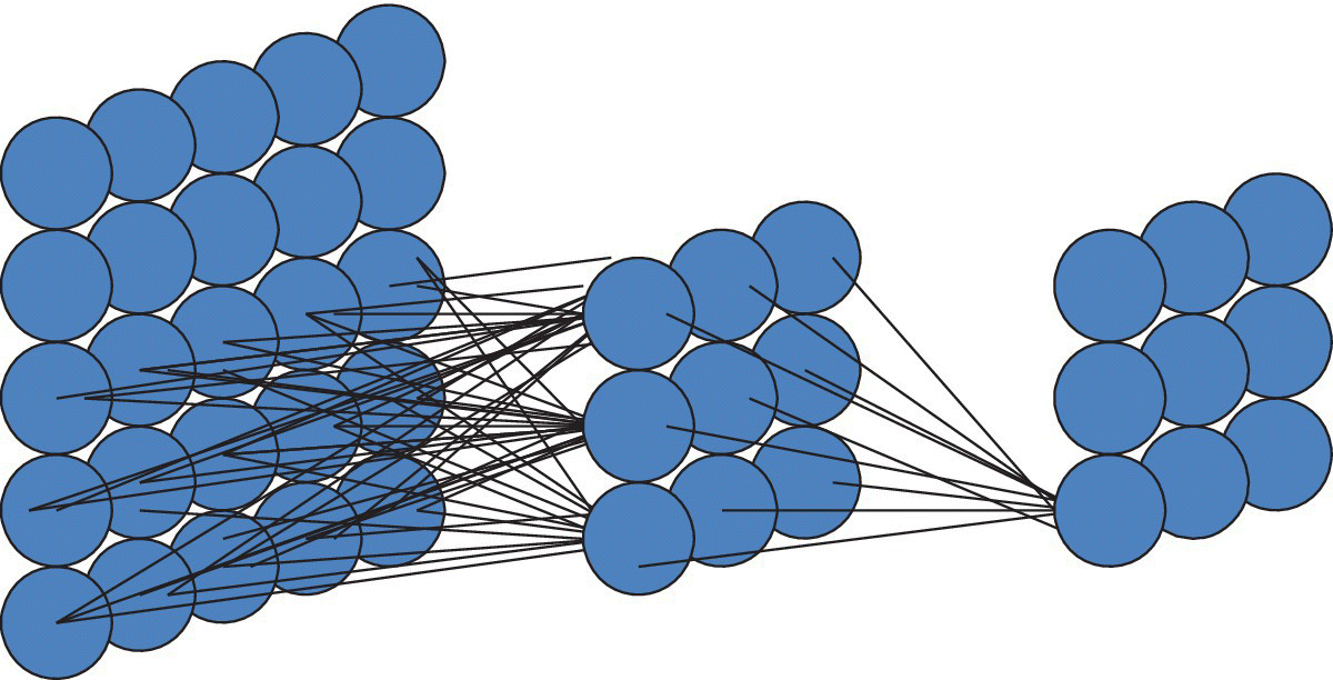
Figure 6.20 Illustration of a convolutional neural net (CNN) convolution layer.
Based on D. Shin et al. (KAIST), ISSCC, February 2017 [20].
For a fully connected layer (FCL) in a CNN, all connections have different weights, as shown in Figure 6.21 (a). In a recurrent neural net (RNN), all connections also have different weights, as shown in Figure 6.21 (b). FCLs and RNNs require a relatively small amount of computation with a huge number of filter weights.

Figure 6.21 Illustration of convolutional neural ets: (a) CNN fully connected layers (FCL) and (b) recurrent neural nets (RNN).
Based on D. Shin et al. (KAIST), ISSCC, February 2017 [20].
This means that different processors are used for convolutional layers (CL) than for fully connected CNN layers and RNNs. When CLs are accelerated with FCL and RL dedicated SoCs they cannot exploit reusability. When FCLs and RLs are accelerated with SoCs specialized for CLs, they suffer from high memory transaction costs, low PE utilization and a mismatch of the computational patterns. Most studies have used different SoCs for the two types of layers. This work studies a combined CNN‐RNN processor, which is highly reconfigurable with high energy efficiency.
This reconfigurable CNN‐RNN processor has three main features: (1) a reconfigurable heterogeneous architecture with a CL processor and an FC‐RL processor to support general purpose DNNs, (2) an LUT‐based reconfigurable multiplier optimized for the dynamic fixed point with on‐chip adaptation to exploit maximum efficiency from kernel reuse in the CP, and (3) a quantization table‐based matrix multiplication to reduce off‐chip memory access and remove duplicated multiplications. The architecture of the deep neural processing unit (DNPU) is shown in Figure 6.22. The part is made using 65 nm CMOS with a 16 mm2 die area. Energy efficiency is 8.1 TOPS/W.
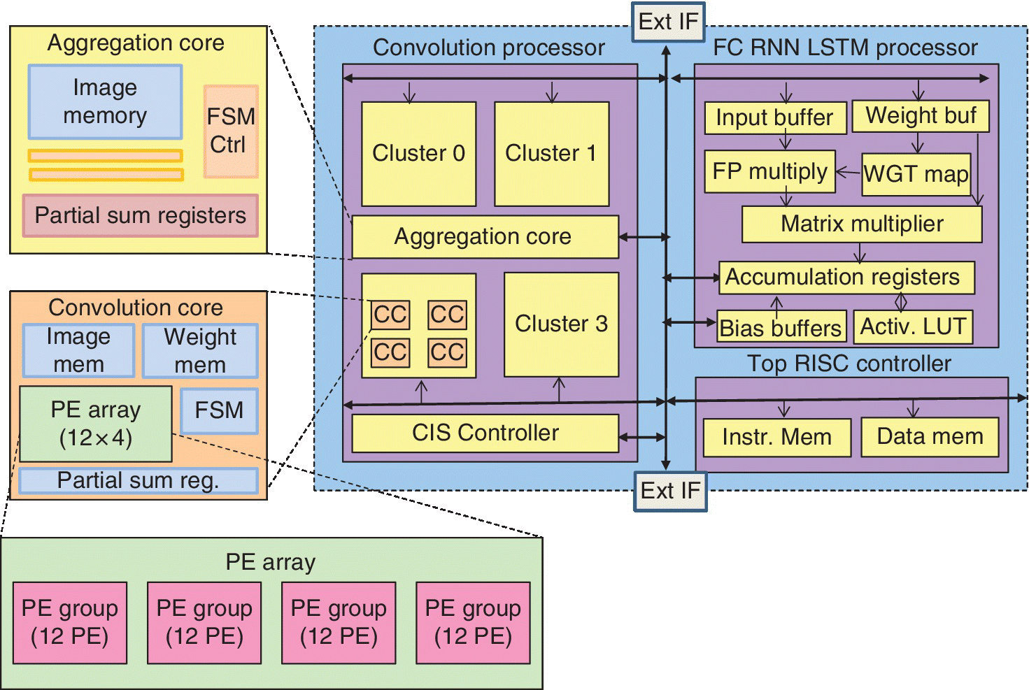
Figure 6.22 Block diagram of deep neural processing unit (DNPU).
Based on D. Shin et al. (KAIST), ISSCC, February 2017 [20].
6.5.2 Deep Neural Nets for Noisy Data
In 2017, Harvard University discussed a 28 nm SoC with a 1.2 GHz sparse deep neural net (DNN) engine for IoT [21]. The SoC is intended for Internet of Things devices to enable the interpretation of the complex and noisy real world data resulting from sensor‐rich systems. Energy efficiency is important. Programmable fully connected deep neural network accelerators have flexible support for general classification talks with high accuracy. Earlier machine learning accelerators have focused either on computer vision CNNs, which consume high power at around 280 mW, or spiking neural networks with low accuracy of about 84% on MNIST.
A 28 nm SoC with a programmable fully connected (FC)‐DNN supported a range of general classification tasks with high accuracy. It offered hardware support for data sparsity by eliminating unnecessary computations that reduced energy. It improved algorithmic error tolerance for weights and datapath computations. It improved circuit level timing violation tolerance and had timing violation detection to reduce energy using Vdd scaling. It had high classification accuracy of 98.36% on MNIST. The accelerator had maximum throughput at 1.2 GHz.
The SoC used an RISC cluster. The DNN engine connected through an asynchronous bridge. A four‐way banked on‐chip memory stored the weights for the DNN model up to 1 MB and had low latency access to the DNN engine. The DNN engine was a five‐stage SIMD‐type programmable sparse matrix vector machine that could process arbitrary DNNs. A sequencer dynamically scheduled operations for the DNN with up to 8 FC layers with up to 1024 nodes per layer. The eight‐way MAC datapath processed eight concurrent neuron computations at a time with 8b or 16b weight precision. A small 512B SRAM buffer kept the list of active node indexes in the previous layer from which W‐MEM addresses are generated.
For MNIST the average loads, operations and cycles were reduced by over 75%, which improved energy and throughput. For the memory, switching activity was reduced so bit‐flips were reduced. A bit‐masking technique was used to mask individual bit errors in the weight word. This permitted the accelerator to tolerate SRAM read timing violation rates at 98.36% accuracy. Timing violation tolerance was improved to 98.36% accuracy over the MNIST test set, which supported VDD reduction to 0.715 V. A system block diagram of the 28 nm SoC with DNN engine is shown in Figure 6.23. Overall energy was reduced by more than nine times using 8 bit weights.
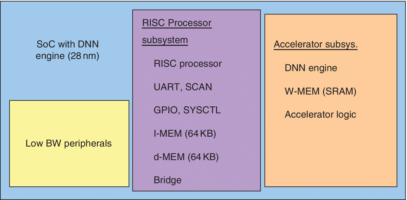
Figure 6.23 System block diagram of 28 nm SoC with deep neural net (DNN) engine for interpretation of noisy real world data from IoT devices.
Based on P. Whatmough et al. (Harvard), ISSCC, February 2017 [21]
6.5.3 Deep Neural Nets for Speech and Vision Recognition
A scalable speech recognizer using hardware accelerated automatic speech recognition (ASR) with deep NN models and voice‐activated power gating for use in personal assistants was discussed in 2017 by MIT and Analog Devices [22]. A wakeup mechanism such as voice activity detection (VAD) is needed to power‐gate the system. ICs for ASR and VAD are described. The power‐gated speech recognizer concept is shown in Figure 6.24. The front end, accoustical models, and neural net search are power‐gated by the VAD detection.

Figure 6.24 Block diagram of power‐gated automatic speech recognition deep neural net chip.
Based on M. Price et al. (MIT, Analog Devices), ISSCC, February 2017 [22].
While most recent work on NN hardware has targeted convolutional networks (CNNs) for computer vision, ICs for keyword detection with DNNs have had power as low as 3.3 mW. This study uses a DNN for low power ASR. The feedforward DNN accelerator uses an SIMD, as shown in the block diagram in Figure 6.25.
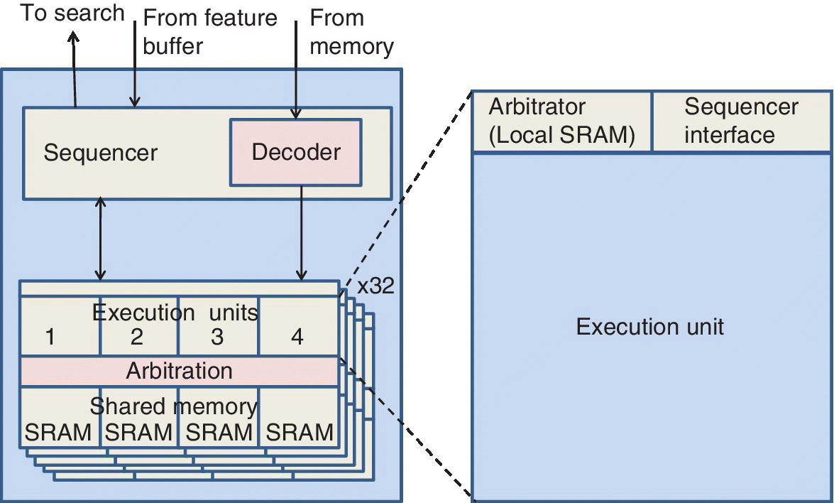
Figure 6.25 Block diagram of feedforward DNN accelerator using an SIMD neural network evaluator.
Based on M. Price et al. (MIT, Analog Devices), ISSCC, February 2017 [22].
The ASR/VAD test chip performed all stages of ASR transcription from audio samples to test using voltages from 0.6 V at 10.2 MHz to 1.2 V at 86.8 MHz. The VAD was functional from 0.5 V at 1.68 MHz to 0.9 V at 47.8 MHz. The core was partitioned into five voltage areas. The SRAM could operate at 0.25 to 0.2 V above the logic supply up to 1.2 V. Latch‐based clock gates were inserted at 76 locations resulting in a 30–40% reduction in core power at full load. Search efficiency varied from 2.5 to 6.3 nJ per hypothesis. A variety of ASR tasks with vocabularies up to 145 words could be run in real‐time. Core power scaled by 45 times.
A 0.26–10 TOPS/W subword parallel convolutional neural net (CNN) processor in 28 nm FD‐SOI technology was discussed in 2017 by KU Leuven [23]. Convolutional neural nets are classification algorithms for visual recognition. They are expensive in terms of energy due to the amount of data movement required and the billions of convolution computations.
This study presents the concept of hierarchical recognition processing using an energy scalable convolutional network processor with efficiencies up to 10 TOPS/W. The processor enables always‐on visual recognition in wearable devices. A block diagram of the top‐level architecture of the processor is shown in Figure 6.26.
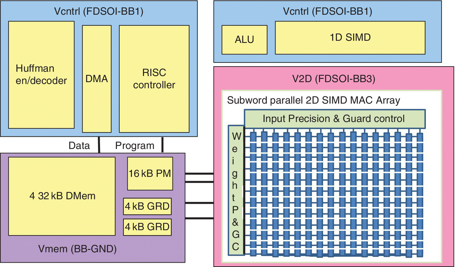
Figure 6.26 Block diagram of top‐level architecture of a CNN processor with efficiencies up to 10 TOPS/W.
Based on B. Moons et al. (KU Leuven), ISSCC, February 2017 [23].
This convolutional network processor allowed use of a wide range of topologies. It had a 16b SIMD RISC instruction set with custom instructions. It was equipped with 2D for convolution, 1D‐SIMD arrays, and a scalar unit. An on‐chip memory used 64 2kB single‐port SRAM macros storing a maximum of 64 K × N words. Three blocks could be read or written in parallel. A six‐stage pipelined processor executed convolutions. A 256b FIFO reduced memory bandwidth by reusing and shifting features along with the x‐axis. All intermediate output values were stored in accumulation registers so there was no data transfer between MACs and no frequent write‐back to SRAM. This 1.87 mm2 chip ran at 200 MHz at 1 V at room temperature. Energy was 6.2 μJ/f at an average 6.5 mW, which shows the potential for always‐on recognition through hierarchical processing.
A 0.52 mW convolutional neural net face recognition processor and a CIS face detector intended for the next generation of wearable devices were discussed in 2017 by KAIST [24]. A face recognition system was developed as a life‐cycle analyzer constantly recording the people encountered together with time and place information. This face recognition had an always‐on capability, which permitted it to be used for user authentication for secure access to personal systems. A convolutional neural network (CNN) was used for high accuracy and to enhance device intelligence. In order for this system to be used with personal devices required that the CNN processors consume low enough power to permit more than 10 hours of operation with a 190 mA h coin battery.
A low power CNN face recognition processor integrated with an always‐on Haar‐like face detector is proposed for smart wearable devices. Three features are used for low power: an analog–digital hybrid Haar‐like face detector for face detection, an ultralow power CNN processor with wire I/O local distributed memory, and a separable filter approximating convolutional layers and a transpose‐read SRAM for low power CNN processing. The system had two chips: a face image sensor and the CNNP. The first provides always‐on face detection. The second completes the facial recognition. The overall block architecture with the face image sensor and the CNN processor is shown in Figure 6.27.

Figure 6.27 Overall block architecture with face image sensor and CNN processor.
Based on K. Bong et al. (KAIST), ISSCC, February 2017 [24].
The overall energy consumption of the facial recognition device was reduced by 39%. The CNN processor could operate at 0.46 to 1.0 V supply with 5 to 100 MHZ clock frequency. The peak power at 0.46 V was 5.3 MW and at 1.0 V was 211 mW. The minimum energy point was 0.46 V. Energy efficiency at MEP is 1.06 nJ/cycle. The proposed system dissipates 0.62 mW on average at a 1 fps frame rate.
A 288 μW programmable deep processor with nonuniform memory hierarchy for mobile intelligence was discussed in 2017 by the University of Michigan and CubeWorks [25]. Recently there has been increased interest in deep learning for mobile IoT. Deep learning has been a powerful tool for applications such as speech and face recognition and object detection.
These are applications that are often needed at the edge of the Internet in situations involving mobile IoT. By having the deep learning at the edge of the Internet, local data can be used and only data for meaningful events need to be forwarded to the Cloud. This has the potential for improving the security of data since it can be secured locally. Many mobile applications are always on, so low power is critical. Rather than focusing on high performance reconfigurable processors optimized for large scale deep neural networks that can consume as much as 50 mW and more, bandwidth and power can be traded off in edge devices. Off‐chip weight storage in DRAM can be avoided since it adds power consumption when data are manipulated in the Cloud due to the intensive off‐chip data movement.
A low power programmable deep learning accelerator (DLA) was proposed with all weights stored on‐chip for mobile intelligence. Low power of less than 300 μW was achieved in four ways: (1) four processing elements were located in the 279KB weight storage memory, which minimized data movement overhead; (2) a non‐uniform memory hierarchy offered a trade‐off between small low power memory banks for frequently used data and larger high density banks for the high power infrequently accessed data and the synaptic weights for the deep learning algorithms can be deterministically scheduled at compilation time using optimal memory assignments, which avoids the need for SRAM caches with their power and area overhead; (3) a 0.6 V 8 T custom memory was specifically designed for DNNs with a sequential access mode, band‐by‐bank drowsy mode control, power‐gating for peripheral circuits, and voltage clamping for data retention; (4) flexible, compact memory storage was achieved using reconfigurable fixed point bit precision from 6 to 32b for neurons and weights. The 40 nm technology deep learning processor included: DLA, RISC processor, and MBus interface, which enabled integration into a complete sensor system. The DLA power was 288 μW at 374 GOPS/W. A top‐level diagram of the DLA is shown Figure 6.28.
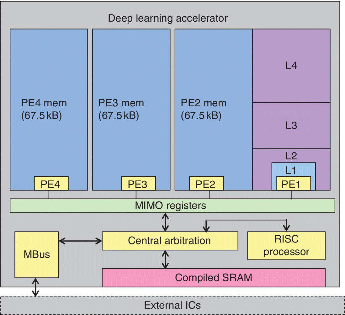
Figure 6.28 Top‐level diagram of the deep learning accelerator (DLA).
Based on S. Bang et al. (University of Michigan, CubeWorks), ISSCC, February 2017 [25].
In the DLA, a nonuniform memory access (NUMA) architecture is used to provide balance between the memory area and access energy. The processor element (PE) NUMA memory floor plan uses signal gating circuits. The SRAM arrays use a dynamic drowsy mode operation since only a few banks are actively accessed in a specific PE while the others are idle most of the operating time. A timing diagram for the SRAM dynamic drowsy mode is shown in Figure 6.29.

Figure 6.29 SRAM synaptic drowsy mode.
Based on S. Bang et al. (University of Michigan, CubeWorks), ISSCC, February 2017 [25].
The 40 nm CMOS test chip measured data access power in L1 at 60% less than in L4. Memory drowsy mode operation reduced leakage by 54% due to peripheral circuits consuming less leakage power. The peak efficiency was 374 GOPS/W at 288 μA at 0.65 V and 3.9 MHz. An application for keyword spotting and face detection was ported on to the DLA. Both DNN classifications fit into the 270kB on‐chip memory with <7 ms latency.
6.5.4 Deep Neural Nets for Other Applications
A 135 mW fully integrated data processor for next‐generation DNA sequencing (NGS) or mapping was discussed in 2017 by National Taiwan University and NCTU [26]. With traditional methods, DNA sequencing is very time consuming, but DNA mapping can be partitioned into suffix array (SA) sorting and backward searching. Dedicated hardware has been proposed for low complexity backward searching but SA sorting has never been implemented. This study discusses a fully integrated NGS data processor that accomplished both SA sorting and backward searching.
A distributed sort algorithm is used to reduce sorting complexity. Throughput for SA sorting is maximized using 2 K insertion sorting elements. Overflow and splitter caches are used to reduce computation latency. This NGS processor achieves several orders of magnitude improvement in energy and throughput compared to high end generic processors. A block diagram of the architecture of the NGS processor is shown in Figure 6.30. Operations in the NGS processor included: splitter reordering, suffix sorting, suffix grouping, parameter analyzing, backward searching, splitter cache, and overflow cache.

Figure 6.30 Block diagram showing architecture of NGS processor.
Based on Y.‐C. Wu et al. (National Taiwan University, NCTU), ISSCC, February 2017 [26].
The 40 nm NGS processor had a chip area of 7.84 mm2 compared to over 300 mm2 for various high end processors also used for DNA analysis. External memory was 1GB and local memory was 384 KB. Operating frequency was 200 MHz compared with over 1000 MHz for comparable alternative processors and power was 135 mW compared to over 4 orders of magnitude for alternative processors. Features of the NGS processor compared favorably with the use of a comparable technology 8‐core processor and 448‐core graphics processor.
References
- 1 Huang, L. et al. (2014) ReRAM‐based 4T2R nonvolatile TCAM with 7× NVM‐stress reduction, and 4× improvement in speed‐word‐length‐capacity for normally‐off instant‐on filter‐based search engines used in big‐data processing (National Tsing Hua University, National Chiao Tung University, NDL, ITRI), VLSI Circuits Symposium, pp. 99, June 2014.
- 2 Chang, M.‐F. et al. (2015) A 3T1R nonvolatile TCAM using MLC ReRAM with sub‐1 ns search time (NTHU, ITRU, NCTU), ISSCC, March 2015.
- 3 Lin, C.C. et al. (2016) A 256b‐wordlength ReRAM‐based TCAM with 1 ns search‐time and 14× improvement in word length‐energy efficiency‐density product using 2.5T1R cell (NTHU, TSMC, NCTU), ISSCC, February 2016.
- 4 Gupta, M. and Hasan, M. (2015) Design of high‐speed energy‐efficient masking error immune PentaMTJ‐based TCAM (Aligarh Muslim Univ.). IEEE Trans. on Magnetics, 51 (2), February 2015
- 5 Wang, X. et al. (2015) Spin‐orbitronics memory device with matching and self‐reference functionality (Avalanche Technology). IEEE Trans. on Magnetics, 51 (11), 1401504, November 2015.
- 6 Bayram, I. and Chen, Y. (2014) NV‐TCAM: Alternative interests and practices in NVM designs (University of Pittsburgh), NVM‐SA, August 2014.
- 7 Lin, W.‐P. (2014) A nonvolatile look‐up table using ReRAM for reconfigurable logic (ITRI, National Taipei University, NTHU, Min Shin University), IEEE Asian Solid‐State Circuits Conference, November 10, 2014.
- 8 Gu, P. et al. (2015) Technological exploration of RRAM crossbar array for matrix‐vector multiplication (Tsinghua University, Arizona State University), ASP‐DAC, January 2015.
- 9 Tanakamaru, S., Yamazawa, H., Tlkutomi, T. et al. (2014) Hybrid storage of ReRAM/TLC NAND Flash with RAID‐5/6 for Cloud data centers (Chuo University, University of Tokyo), IEEE ISSCC, February 2014.
- 10 Xu, C. et al. (2015) Overcoming the challenges of crossbar resistive memory architectures (Oakridge National Laboratory), HPCA, February 2015.
- 11 Vincent, A.F. et al. (2014) Spin‐transfer torque magnetic memory as a stochastic memristive synapse (University of Paris‐Sud, CNRS, CEA, LIST), ISCAS, pp. 1074, June 1, 2014.
- 12 Vincent, A. et al. (2015) Spin‐transfer torque magnetic memory as a stochastic memristive synapse for neuromorphic systems (University of Paris‐Sud, CEA, Beihang University). IEEE Trans. on Biomedical Circuits and Systems, 9 (2), April 2015.
- 13 Zhang, D. et al. (2016) All spin artificial neural networks based on compound spintronic synapse and neuron (Beihang University, University of Paris‐Sud, Tsinghua University). IEEE Trans. on Biomedical Circuits and Systems, 10 (4), August 2016.
- 14 Chen, P. and Yu, S. (2016) Partition SRAM and RRAM based synaptic arrays for neuro‐inspired computing (Arizona State University), ISCAS, May 2016.
- 15 Suri, M. and Parmar, V. (2015) Exploiting intrinsic variability of filamentary resistive memory for extreme learning machine architectures (IIT New Delhi). IEEE Trans. on Nanotechnology, 14 (6), November 2015.
- 16 Suri, M. et al. (2015) Neuromorphic hybrid RRAM‐CMOS RBM architecture (IIT, IEF‐CNRS, IEMN‐CNRS), 15th NVMTS, October 2015.
- 17 Eryilmaz, S. et al. (2016) Training a probabilistic graphical model with resistive switching electronic synapses (Stanford, University of California at Irvine, University of California at San Diego, IBM, Macronix). IEEE Trans. on Electron Devices, 63 (12), December 2016.
- 18 Shelby, R.M. et al. (2015) Non‐volatile memory as hardware synapse in neuromorphic computing: a first look at reliability issues (IBM), IRPS, April 2015.
- 19 Desoli, G. et al. (2017) A 2.9TOPS/W deep convolutional neural network SoC in FD‐SOI 28 nm for intelligent embedded systems (STMicro), ISSCC, February 2017.
- 20 Shin, D. et al. (2017) DNPU: An 8.1TOPS/W reconfigurable CNN‐RNN processor for general‐purpose deep neural networks (KAIST), ISSCC, February 2017.
- 21 Whatmough, P. et al. (2017) A 28 nm SoC with a 1.2 GHz 568 nJ/prediction sparse deep‐neural‐network engine with >0.1 timing error rate tolerance for IoT applications (Harvard), ISSCC, February 2017.
- 22 Price, M., Glass, J. and Chandrakasan, A. (2017) A scalable speech recognizer with deep‐neural‐network acoustic models and voice‐activated power gating (MIT, Analog Devices), ISSCC, February 2017.
- 23 Moons, B. et al. (2017) ENVISION: A 0.26‐to‐10 TOPS/W subword‐parallel dynamic‐voltage‐accuracy‐frequency‐scalable convolutional neural network processor in 28 nm FDSOI (KU Leuven), ISSCC, February 2017.
- 24 Bong, K. et al. (2017) A 0.62 mW ultra‐low‐power convolutional‐neural‐network face‐recognition processor and a CIS integrated with always‐on Haar‐like face detector (KAIST), ISSCC, February 2017.
- 25 Bang, S. et al. (2017) A 288 μW programmable deep‐learning processor with 270 KB on‐hhip weight storage using non‐uniform memory hierarchy for mobile intelligence, ISSCC, February 2017.
- 26 Wu, Y.‐C. Hung, J.‐H. and Yang, C.H. (2017) A 135 mW fully integrated data processor for next‐generation sequencing (National Taiwan University, National Chiao Tung University), ISSCC, February 2017.