
5
Neuromorphic Computing Using Emerging NV Memory Devices
5.1 Overview of Resistive RAMs and Ferroelectric RAMs in Neuromorphic Systems
Neural network systems, imitating the human brain, are also a type of interconnected network and use many of the same low cost, low power types of devices as other smart networks. Neural networks can require multilevel, analog like, memory devices as synapses connecting neurons. These single neuromorphic chips can be used for data processing in applications such as voice and vision recognition at the edge of the Internet of Things. Local intelligent nodes can analyze local data and send the results on providing an extra level of data security.
Various types of resistive RAMs (RRAMs) and ferroelectric RAMs (FeRAMs) have been used in artificial neural networks. These technologies can emulate synaptic plasticity and learning rules such as spike‐timing dependent plasticity (STDP) in which the synapses, which are connections between neurons, are altered in response to stimulus. The persistence of this change enables learning, that is, synaptic changes are persistent so the network state can be reactivated and stimulated further later. The multivalue property of RRAMs can be increasing or decreasing. When used as a synapse in a neural net, if the conductance is increasing, the property is called potentiation, and if the conductance is decreasing, the property is called depression.
Direct mapping can be provided using learning algorithms. The low power consumption of RRAMs and their plasticity or multivalue properties make them promising for implementing synaptic behavior in complex systems.
5.2 Various Resistive RAMs for use as Synapses in Neuromorphic Systems
5.2.1 Metal Oxide Resistive RAM (MO‐RRAMs) as Synapses
Metal oxide RRAM cells consist of a metal–insulator–metal (MIM) structure where the insulator can undergo abrupt switching into a conductive state and gradual switching into a nonconductive state. This resistive switching is related to the reversible formation and disruption of a conductive filament (CF), which provides a shunt for the top and bottom electrodes through the insulating layer. The CF formation and dissolution can be related to the displacement of oxygen atoms.
In June of 2014, Arizona State University discussed using a metal oxide RRAM (MO‐RRAM) as a synaptic device for a hardware implementation of neuromorphic computing [1]. The gradual resistance modulation capability in RRAM can emulate analog synapses and the stochastic switching behavior of the RRAM could emulate binary synapses. Neuromorphic computing is of interest since it uses massive parallelism from distributed computing and localized storage in neural networks. Its error tolerance is interesting for use in vision and speech recognition. Neuromorphic computing can be run in a conventional digital computer enabled by software. Two terminal RRAMs can be used as artificial synapses. Metal oxide RRAM is interesting for neuromorphic systems due to low energy consumption, compatibility with CMOS technology, and potential for Gbit density through 3D integration.
A hybrid neuromorphic system with CMOS neurons and RRAM synapses was demonstrated. During RESET a conductive filament (CF) is ruptured and a variable tunnel gap forms between an electrode and the residual filament. The variation in tunnel gap results in multilevel resistance states. The SET is abrupt. Resistance versus number of voltage pulses is shown Figure 5.1 for (a) an abrupt SET and (b) a gradual RESET.
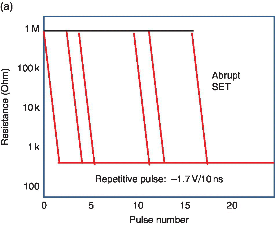
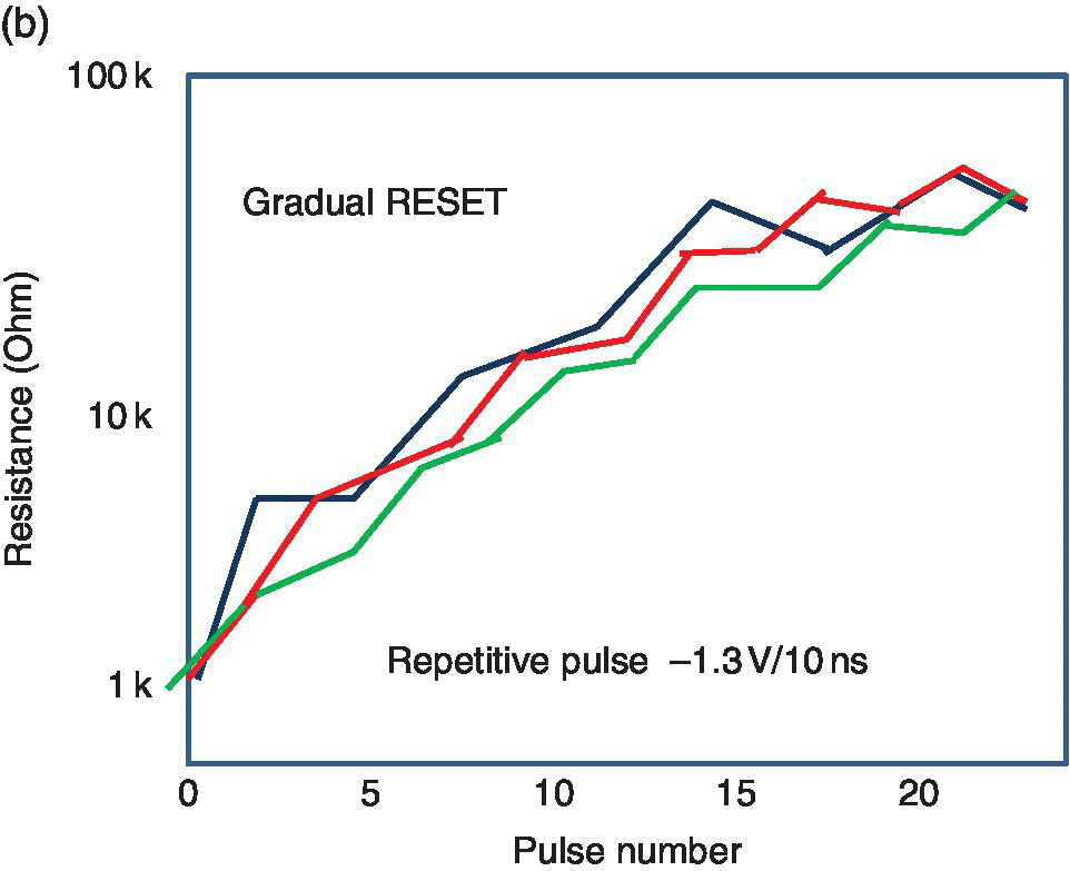
Figure 5.1 Resistance versus pulse number for an MO‐RRAM: (a) an abrupt SET and (b) a gradual RESET operation.
Based on S. Yu (ASU), ISCAS, June 2014 [1].
The RRAM can function as the analog synapse using the gradual RESET and the binary synapse using the stochastic SET for competitive learning. A simulation of a winner‐take‐all network for an orientation classification function was discussed. Comparable system performance was shown between the analog synapse and the binary synapse.
Any resistive memory with multilevel characteristics can be used as a synaptic device in a neuromorphic computing system. In 2016 POSTECH [2] investigated abruptly formed filaments and found this abrupt formation degrades analog switching behavior during potentiation. By using a balanced SET/RESET pulse operation and modulating the switching gap to control the filament growth, the conductance behavior could be gradually changed.
An HfO2‐based RRAM array with multilevel states under a constant pulse was shown to have a controlled filament. The RRAM cell had a TiN/HfO2/Ti/TiN stack made on top of a transistor in an 8 inch wafer process. An I–V curve under 100 μA with 1.2 V was found. A conductive filament (CF) of oxygen vacancies (ions) was formed under positive bias and gradually dissolved with negative bias. This resulted in a switching gap between the CF and the bottom electrode.
Synaptic behavior was evaluated by applying successive identical pulses. The multilevel states of conductance were observed in depression and a binary state was shown during potentiation. Synaptic behavior was demonstrated. A schematic illustration of a plausible mechanism is shown in Figure 5.2. Figure 5.2 (a) shows the initial filament (SET) while Figure 5.2 (b) shows a RESET with a partially ruptured conductive filament. Figure 5.2 (c) represents the second SET showing a thicker conductive filament.

Figure 5.2 Schematic illustration of plausible mechanism of multilevel states of conductance: (a) initial filament (SET), (b) RESET with partially ruptured conductive filament, and (c) second SET with thicker conductive filament.
Based on J. Woo et al. (POSTECH), SNW, June 2016 [2].
In August of 2016, POSTECH discussed improving synaptic behavior of a neuromorphic system using identical pulses on a filamentary AlO x /HfO2 bilayer RRAM array to emulate the synaptic function [3]. It was found that the multilevel states of conductance were attained by varying measurement conditions for the formation and rupture of a conductive filament.
A TiN/HfO2/Ti/TiN stack was used for the RRAM. Multiple current states were found by either varying the RESET voltage from –0.7 to –1.9 V with a step voltage of –0.05 V negatively or varying the gate voltage from 0.6 to 1.2 V with a step voltage of 0.05 V positively.
Abrupt switching was found to lead to an unchanged conductance state causing degradation in the accuracy of pattern recognition. A linear potentiation or depression behavior of conductance was shown by applying identical pulses using the effect of a barrier layer on switching. This was done by making an RRAM on top of an Al electrode. It was found that when the range of conductance was symmetrically controlled at both polarities improved accuracy was achieved for pattern recognition using a neural network.
An optimized programming method for linear potentiation in a filamentary HfO2 RRAM synapse intended for use in a neuromorphic system was discussed by POSTECH in December of 2016 [4]. Various programming methods were used to linearly change the resistance state with either SET voltage/pulse ramping or Gate voltage ramping. The results showed that the multilevel cell (MLC) was related to the size of the conductive filament where the oxygen vacancies moved under the influence of applied pulses. By optimizing the pulse for a given condition, such as identical pulses, it was possible to linearly increase the MLC behavior, which enabled pattern recognition accuracy in neuromorphic systems.
For proper operation of an RRAM synaptic device, a monotonic increase or decrease of the MLC characteristics should be expected. Recent studies have, however, focused on the use of gradually transited MLC in depression with abrupt formation of conductive filament in potentiation. This asymmetric MLC behavior tends to lead to a degradation of pattern recognition accuracy. A possible solution is two identical synaptic devices serving as a single synapse, but this consumes a large amount of power per area.
An alternative solution is linearly increased MLC behavior in potentiation and in depression. This was achieved by using different pulse methods for potentiation and for depression. A CMOS compatible TiN/HfO2/Ti/TiN RRAM structure was used with a 0.35 µm transistor for a 1T1R configuration in a 200 mm wafer process. During potentiation, the gate voltage is ramped at a fixed set voltage. The increased currents are proportional to the large gate voltage due to the thickness of the filament formation. Ramping the gate voltage at a fixed SET voltage results in an MLC operation during potentiation due to thickening of the filament.
For depression, an optimized RESET pulse can lead to dissolving the conductive filament with a particular switching gap, which enables intermediate states as a result of varying partially dissolved conductive filament gaps. As a result, MLC operation with varied programming schemes during potentiation resulted in MLC states during potentiation and depression, which improved the accuracy for pattern recognition applications in neuromorphic systems.
5.2.2 Conductive Bridge RRAM (CB‐RRAM) as Synapses
In the case of conductive bridge RRAMs (CB‐RAM) cells, the CF formation and dissolution is related to metal ions. Both CB‐RAMs and MO‐RRAM cells have low operating voltages, fast programming, nanoseconds of read time, low power consumption, scalability, and endurance that is higher than conventional Flash memory.
Various trade‐offs exist between the memory window and endurance and the memory window and switching time. The low resistance state (LRS) when the CF is fully formed is modulated by the compliance current, which is applied so the higher the programming current the thicker the CF and the lower the resistance state. In 2015, CEA LETI described an example of an MO RRAM and a CB‐RAM for use as synapses [5]. The MO RRAM was formed by two electrodes, in this case, one Ti and one TiN with an HfO2 insulating layer between them. The CB‐RAM was formed with a W/HfO2 electrode and an Ag or Cu electrode with a GeS2 electrolyte between them. In the case of the CB‐RAM, the CF will be formed of Ag or Cu atoms. Schematic cross‐sections of the MO RRAM and a CBRAM are shown in Figure 5.3.

Figure 5.3 Schematic cross‐sections of (a) a metal oxide MO‐RAM in 28 nm CMOS and (b) a CB‐RAM in 130 nm CMOS.
Based on B. DeSalvo et al. (CEA LETI), IMW, May 2015 [5].
The multilevel capability of a solid electrolyte RRAM, a form of conductive bridge RAM (CB‐RAM), was explored for use as a synapse device by several Chinese and Taiwanese Universities in August of 2015 [6]. The device used a Pt/GeSO/TiN structure. The cut‐off voltage was varied during the I–V cycles, resulting in continuous multilevel conductance states. It was also possible to vary the AC pulse programming and voltage amplitudes to obtain multilevel states. It was noted that arithmetic operations based on analog memories may also be an interesting computational paradigm to complement digital von Neumann systems. An electronic synapse device was made with a Pt/GeSO/TiN thin film stack. The 16 nm thick switching layer was RF magnetron sputtered on to a TiN/Ti/SiO2/Si substrate. The multilevel bipolar resistance switching I–V curves of the Pt/GeSO/TiN device are shown in the diagram in Figure 5.4.
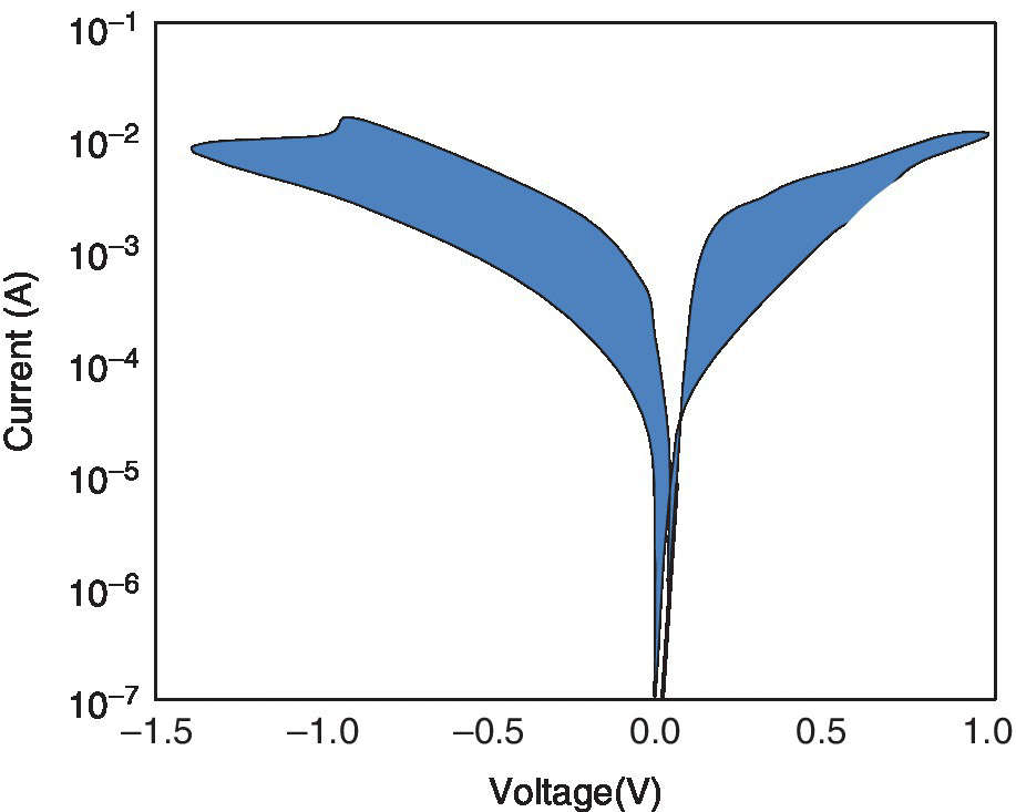
Figure 5.4 I–V curve for electronic synapse CBRAM device using Pt/GeSO/TiN Stack with gradually increasing set pulse voltages and pulse widths resulting in a continuous multilevel effect, Based on W. Zhang (Xidian University, NCKU, National Sun Yet‐sen University, Xiamen University, NCTU), IEEE Electron Device Letters, August 2015 [6].
A series of gradually increasing set pulse voltages and pulse widths were applied to the Pt/GeSO/TiN device and the conductance gradually increased with increasing pulse voltage and pulse width. The multiple levels are shown as nearly continuous. This multilevel effect can be useful in systems emulating biological synapses.
Certain characteristics are important when investigating the capability of the device to emulate adaptive learning in biological synapses. In a biological synapse, when the pre‐spike signal precedes the post‐spike signal, the strength of the synapse undergoes long term potentiation (LTP) or increase; otherwise it undergoes long term depression (LTD) or decrease. Closer timing spikes lead to a larger change of feedback. This is called the spike timing‐dependent plasticity (STDP) learning rule, which has been shown in various brain circuits for many species of creature. STDP learning was confirmed in this CBRAM device.
5.2.3 Phase Change Memory (PCM) as Synapses
Technologies for brain‐type computing intended to overcome implementation issues for neural networks can also use resistive memory such as phase change memory (PCM). These programmable resistive RAMs were used in March of 2014 by CEA‐LETI, CEA‐LIST, and InRIA to obtain low area synapses [7]. PCM are made of chalcogenide glass material, which can be either in an amorphous or a crystalline state depending on the rate of heating and cooling of the material. The crystalline phase has a lower resistivity than the amorphous phase, which results in a resistive RAM with multiple states that can be used as variable state synapses.
Through‐silicon‐vias (TSV) were used with the PCM in this demonstration to improve analog neuron connections, reduce their area, and improve connectivity. The conductance of the PCM is modulated by the heat from the current flowing through the PCM devices. These devices were used to produce arrays of artificial synapses.
A 2‐PCM synapse was discussed that emulated synaptic functions in large scale neural networks. The two PCM devices had opposite contributions to the neuron integration. Partial crystallization of the phase change material of one PCM was used to increase the equivalent weight of the synapse and partial crystallization of the other to decrease it.
5.2.4 PCMO RRAM as Synapses
A Pr0.7Ca0.3MnO3 (PCMO) RRAM‐based synaptic device for neuromorphic computing was developed in 2014 by Pohang University of Science and Technology (POSTECH) and the Gwangju Institute of Science and Technology [8]. Thin film elements of PCMO can be made with thicknesses down to a few tens of nanometers. A wafer scale device was made and showed good switching uniformity and analog memory behavior. Figure 5.5 shows bipolar I–V curves at different sweep voltages, illustrating the possibility of analog memory behavior.
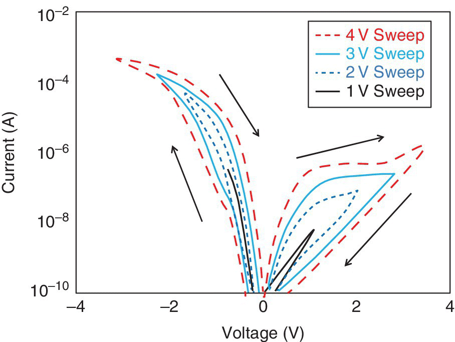
Figure 5.5 Illustration of RRAM I–V curves at different sweep voltages showing potential for analog behavior of a PCMO RRAM.
(Based on J. Jang et al. (Pohang University, Gwangju Institute of Science and Technology), ISCAS, June 2014 [8].
The PCMO‐RRAM was used to implement analog artificial synapse characteristics in neuromorphic systems. A face recognition function was used to show varying potentiation and depression characteristics of the RRAM synapse. Figure 5.6 shows potentiation and depression curves. Potentiation voltage is –3 V and depression voltage is +3 V.

Figure 5.6 Illustration of potentiation and depression curves for PCMO‐RRAM. Potentiation voltage is –3 V and depression voltage is +3 V.
Based on J. Jang et al. (Pohang University, Gwangju Institute of Science and Technology), ISCAS, June 2014 [8].
Simulations were performed for time series prediction and face recognition applications based on a proposed RRAM synaptic device model. A multilayer neuromorphic architecture was designed. The architecture consisted of 408 CMOS neurons and 83 200 RRAM synapses. For negative synaptic weight implementation, two RRAM synaptic devices were used as one synapse.
In May of 2015, POSTECH, Gwangju Institute of S&T, and IBM discussed the optimization of conductance change behavior in analog resistive memory synaptic devices based on PrCaMnO3 (PCMO) [9]. In this study, resistive memory based on PCMO is applied in a neural network application, which is classification of the MNIST handwritten digits using a multilayer perceptron trained with back propagation under a variety of simulated conductance change behaviors. Linear and symmetric conductance changes during increasing and decreasing device conductance are shown to offer the highest classification accuracies. Additional improvements could be obtained using nonidentical training pulses at the cost of requiring measurement of individual conductance during training. Using PCMO‐based synaptic devices, a generalization accuracy on a previously unseen test set was 90.55%.
PCMO RRAM memory arrays of 1‐Kbit were made to evaluate synaptic devices. The device stack had a 50 nm thick Pt bottom electrode, with 30 nm deposited polycrystalline PCMO film patterned with conventional lithography and reactive ion etching (RIE), followed by an 80 nm thick SiN x layer. The switching behavior of an RRAM based on this PCMO stack was determined and neural network simulations were done using its conductance change behavior. Handwriting digit classification accuracies were found to be high for RRAM‐based synaptic devices with symmetric switching behavior. They are maximized when that response is linear.
In August of 2016, POSTECH, Gwangju Institute of S&T, and IMEC discussed an analog synapse PCMO‐based interface switching device with varying electrode materials [10]. It was compared with a filamentary switching device having 1‐bit storage and variability issues. The interface switching devices showed good electrical properties, which included 5‐bit (32 level) multilevel cell characteristics along with wafer scale switching uniformity and scalability of switching energy with device area. An Mo electrode was proposed to improve data retention of the interface switching device. The Mo electrode increased the oxidation barrier height to 0.4 eV, which improved the retention time and pattern classification accuracy of the neural networks.
A 10 nm thick polycrystalline PCMO film was deposited on a Pt/Ti/SiO2/Si wafer using RF sputtering. A 100 nm SiNx vertical side wall was deposited by plasma‐enhanced CVD and then dry etched using RIE with a 150 nm via‐hole structure. Various top electrodes were used including: Al, Ti, Ta, and Mo. The data retention characteristics and switching uniformity of the basic interface RRAM were studied with varying electrode materials for synapse applications. Using neural network simulations it was confirmed that data retention characteristics were critical to guarantee the pattern classification accuracy.
An Mo/PCMO synapse device was reported with good wafer scale switching uniformity, multilevel data storage capability, and good retention characteristics. The improved LRS retention characteristics were explained by the high activation energy of the oxidation process and high electronegativity of the Mo electrode. It was confirmed that an improvement in data retention directly affected the pattern classification accuracy of the neural network.
5.2.5 RRAM with Simultaneous Potentiation and Depression
A homogeneous barrier modulation (HBM) RRAM that was capable of a simultaneous potentiation (P) and depression (D) was described in October of 2015 by National Chiao Tung University [11]. A simulation of pattern learning algorithm was performed based on the winner‐take‐all rule and on experimental synaptic characteristics. A circuit diagram of the simulated neuromorphic system and applied signal waveforms is shown Figure 5.7.

Figure 5.7 Schematic circuit of simulated neuromorphic system with applied signal waveforms.
Based on Chou et al. (NCTU), VLSI‐TSA, April 2015 [11].
The winner‐take‐all learning rule was applied to update the synaptic weight of each synapse through training. This clock‐synchronized system included two phases: (1) training during which one set of training voltage patterns was sent into the synapse array by pre‐neurons (column) while post‐neurons (row) sum up the current through the synaptic cells in every column and (2) fireback during which voltage patterns of pre‐neurons were inverted and only the post‐neuron that sums the largest amount of current during (1) fired a large but shorter pulse back into the same column. The combinational effects are designed to potentiate or depress synaptic weights of the cells on the fired column toward lower or higher resistance according to the 1/0 of the training patterns.
The potentiation plus depression (P + D) method improved the contrast development of pattern learning and immunity to input noise compared with the P‐only method. The recent fast development of RRAMs has inspired several attempts to use them as the high density electronic synapses in artificial neuromorphic systems. This study reported on a homogeneous barrier modulation (HBM) RRAM that was capable of a simultaneous P and D operational scheme. The RRAM stack was SiO2/Ti/TiO2(30 nm)/TaO2(10 nm)/Ta/BE.
5.2.6 Other Nonvolatile Memories with Analog Properties
An example of potentiation and depression in a memory using a measurement of capacitance rather than resistance was illustrated in February of 2015 by Seoul National University and Samsung [12]. A silicon‐based charge trap memory with an Al/HfO2/Al2O3/Si2N4/Si stack was used, which emulated that memory function of a biological synapse. The quantity of the trapped charge in the proposed Al2O3/HfO2/Si3N4 stack was estimated by measuring the capacitance over time with different repeated input pulses, which are similar to the behavior of a biological synapse and were regarded as representing synaptic weight changes. By applying repeated voltage pulses at periodic intervals at different times, reliable short term plasticity and long term potentiation properties were found along with their transition behavior. This architecture was found to be compatible with a CMOS process and had promise of being possible to implement in an electrical neuromorphic system.
The fabricated device consisted of an Al gate electrode and an Al2O3/HfO2/Si3N4 gate stack formed on a p‐type silicon (100) wafer. Initially an n+ region was formed with As+ ions and annealed to supply electrons to the gate stack during programming. Then HfO2 layers and Al2O3 layers were formed by ALD at 350 °C. An Al layer was then deposited and patterned to form the top electrode. The area of the Al electrode is about 100 × 100 µm2. Programming was done at 7 V for 1 ms and erased at –7 V for 1 ms. An energy band diagram of an Si/Si3N4/HfO2/Al2O3/Al cell is shown in the diagram in Figure 5.8. CV measurements were used in an effort to imitate synaptic plasticity. The competing effect of memory loss and memory strengthening was observed in repeated simulations.
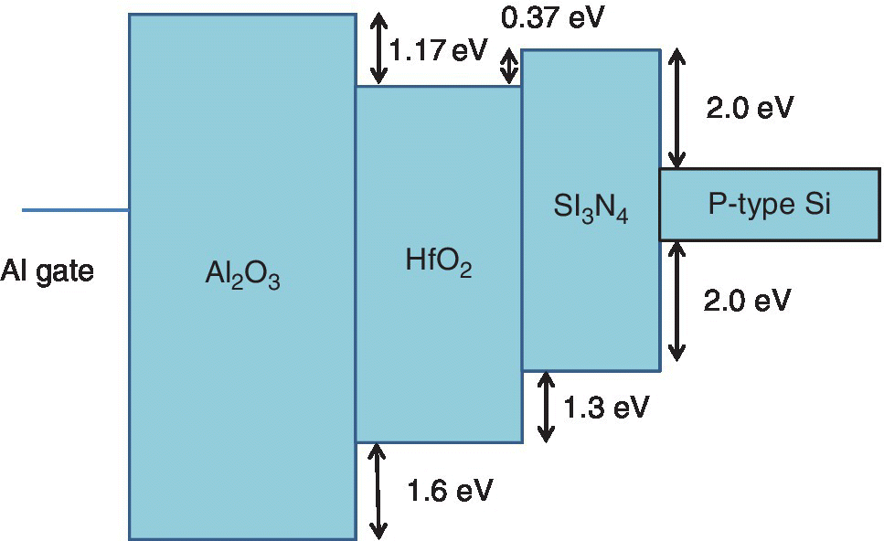
Figure 5.8 Energy band diagram of Si/Si3N4/HfO2/Al2O3/Al cell.
Based on M.‐S. Lee et al., IEEE Trans. on Electron Devices, February 2015 [12].
An amorphous silicon‐based metal–semiconductor–metal (MSM) device can be used as a resistive switching device or a neuron in a neuromorphic computing system. In 2015 Carnegie Mellon University showed that CMOS compatible Pt/a‐Si/Cu stacks show negative differential resistance (NDR) that enables their operation as oscillatory elements and nonlinear threshold switches [13]. To demonstrate oscillations in amorphous silicon (a‐Si), this study showed frequency tunability from 5 kHz to 80 MHz by modulating the series ballast and changing the source voltage. The devices showed <1.2 V and <100 μW operation. As threshold switches, these devices showed an ON/OFF resistance >800 with a peak current density of > 0.3 MA cm2 at 1 V. The change in modes of operation of the device was studied as a threshold switch and an oscillator.
5.3 3D Neuromorphic Memories
5.3.1 Neuromorphic Architectures as Dense TSV 3D Structures
Neuromorphic architectures are 3D structures with massive parallelism. They exhibit a high level of connectivity. Deep computation and cognitive functions reach thousands of neurons and millions of synapses. It is assumed, therefore, that the neural network must be multilayer and densely connected using point‐to‐point connectivity. 3D architectures are therefore expected to reduce routing congestion, reduce critical path length, and save area and power.
The network studied by CEA and associated labs in 2014 was a neural processor with two layers of densely connected networks using through silicon via (TSV) intended to recognize objects appearing in a 1000 frame/s video stream [7]. The target operation was executing complex tasks. Two separate circuits were designed for face‐to‐face connections. Short TSVs could be used to bond the last metal layers of both circuits and longer TSVs could be used that cross all metal layers. In 3D monolithic integration, transistor layers are made one on top of the other on the same die. An example of transistor level monolithic 3D integration is shown in Figure 5.9.
Figure 5.9 Example of 3D transistor level monolithic integration.
Based on F. Clermidy et al. (CEA‐LETI, CEA‐LIST, INRIA), ASP‐DAC, January 2014 [7].
Another dense 3D synaptic architecture using a self‐rectifying bipolar Ta/TaOx /TiO2/Ti RRAM stack was described in December of 2014 by NCTU [14]. This RRAM device showed good analog synaptic features. Ultralow energy consumption was shown, which was comparable to that of a biological synapse at <10 fJ/spike. Several synaptic features were demonstrated using a Ta/TaOx /TiO2/Ti RRAM synaptic element. The analog synaptic characteristics were modeled using physical and compact models. SET controlled and RESET controlled multilevel cell (MLC) operations for the 2D Ta/TaOx /TiO2/Ti RRAM device were shown. By varying V set or V reset, multiple resistance states could be read out at –2 V. A very low current was found at a positive voltage bias.
5.3.2 3D Vertical RRAMs as Synapses Connecting Neurons
A number of vertical 3D RRAM arrays have been described for use in neuromorphic applications. The RRAM element that exhibits analog conductance behavior acts as a synapse connecting parallel input and output neurons. In July of 2014, the University of Michigan discussed a 3D vertical two‐layer RRAM with well characterized analog switching characteristics for use in neuromorphic computing applications [15]. The dual‐layer RRAMs had a WOx switching layer, which was formed at the sidewall of horizontal electrodes. The devices showed well characterized analog switching characteristics and a very small mismatch in electrical characteristics between devices formed in the two layers, as shown in Figure 5.10, which is a schematic of current output versus time for the upper and lower device.
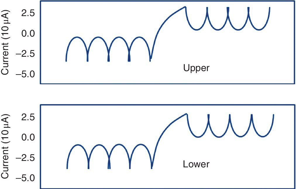
Figure 5.10 Current output versus time for upper and lower devices illustrating good matching between the two.
Based on S. Gaba et al. (University of Michigan), IEEE Trans. on Electron Devices, July 2014 [15].
The 3D vertical device structure allowed higher storage density and bigger connectivity for use in neuromorphic computing. The vertical devices were shown to have potentiation and depression characteristics similar to planar RRAMs. The two layers could be programmed independently with no crosstalk seen between the layers.
The devices could be programmed with <10% mismatch. The architecture was considered scalable and suitable for development of analog memory and neuromorphic systems. During write and erase a V/2 method could be used to avoid disturbing unselected bit‐lines and word‐lines. During READ, grounding methods could be used to avoid sneak path currents. The I–V characteristic was nonlinear, which was expected to improve the read margin as the array size scaled. The conductance change ratio and switching speed may be improved further by optimizing the various process steps.
In December of 2015 various French labs investigated the vertical pillar RRAM (VRRAM) concept for use in neuromorphic applications [16]. In this case, one synapse was emulated by one VRRAM pillar. The basic functionality of the HfO2‐based MO‐VRRAM was given as 20 ns switching time, up to 107 cycles with stable 200 °C data retention. Specific analyses were made of the resistance and switching voltage variability to conveniently address the various potentiation applications. A correlation effect was found to exist between adjacent cycles. This was taken to mean that the conductive filament keeps a memory of its shape in the previous state, which leads to reduced cycle‐to‐cycle variability in a sufficiently short cycle range. A compact model and circuit simulations were used to propose the VRRAM for convolutional neural network applications. Reliability was good and of lesser circuit complexity than planar approaches.
The VRRAM device used a TiN/SiO2 double layer deposited on a vertical W plug. The TiN thickness was 10 nm. The cylinder was formed using a plasma etch to pattern it. An nMOS transistor was used as the selector for the memory. An analog‐like conductance behavior was due to the variability of an oxide‐based RRAM. A model was used to simulate a synapse composed of stacked VRRAMs with from 2 to 24 levels. The VRRAMs were addressed simultaneously and the output signal corresponded to the sum of all the VRRAMs in parallel. A simulated neuromorphic array is shown in Figure 5.11. A synapse is composed of “N” VRRAM cells in a vertical pillar, which are addressed in parallel. The output neuron collects the contributions of all the synapses.

Figure 5.11 Simulated neuromorphic network showing synapse of “N” VRRAM cells.
Based on G. Piccolboni et al. (CEA, LETI, Minatec, IM2NP, IMEP‐LAHC), IEDM, December 2015 [16].
The vertical pillar RRAM used for neuromorphic applications was shown again in 2016 by CEA and various associated labs [17]. An Al2O3/Cu CB‐RAM was used in a vertical configuration for neuromorphic applications. Each cell constituted a vertical synapse. A selector and array configuration was tuned to reduce the variability of voltage seen by each cell. A circuit was designed to implement a neuromorphic system. The neural circuit scheme is shown in Figure 5.12, where vertical‐CBRAM pillars have m levels. All levels share a common transistor. Each pillar has a transistor with an n × wider channel compared to plane select transistors.

Figure 5.12 Neural circuit with V‐CBRAM pillars having m levels sharing a common transistor.
Based on G. Piccolboni et al. (CEA, LETI, Minatec), IMW, May 2016 [17].
The synapses are emulated by 1TnR VRRAM pillars, which share a transistor per level. One transistor per pillar is used to select the pillar itself and no back‐end selector is required. In a worst case, a given CBRAM on a selected pillar has to be SET while all the other CBRAM on the selected pillar are LRS. All other pillars are left floating to cancel any sneak path current on other CBRAMs so their influences can be neglected. The main issue is the voltage difference V te–V be seen by the V‐CBRAM in the LRS state serially connected to the line access transistor on an m‐levels selected pillar. The SET condition can be studied as a function of the number m of VRRAM on a pillar and the oversize factor n of the access transistor.
The actual implementation in silicon of such a vertical pillar structure was shown in 2016 by Stanford University, NNDL, and Narlabs, who discussed a four‐layer 3D vertical RRAM integrated with a FinFET [18]. A schematic cross‐section of the 3D RRAM is shown Figure 5.13.
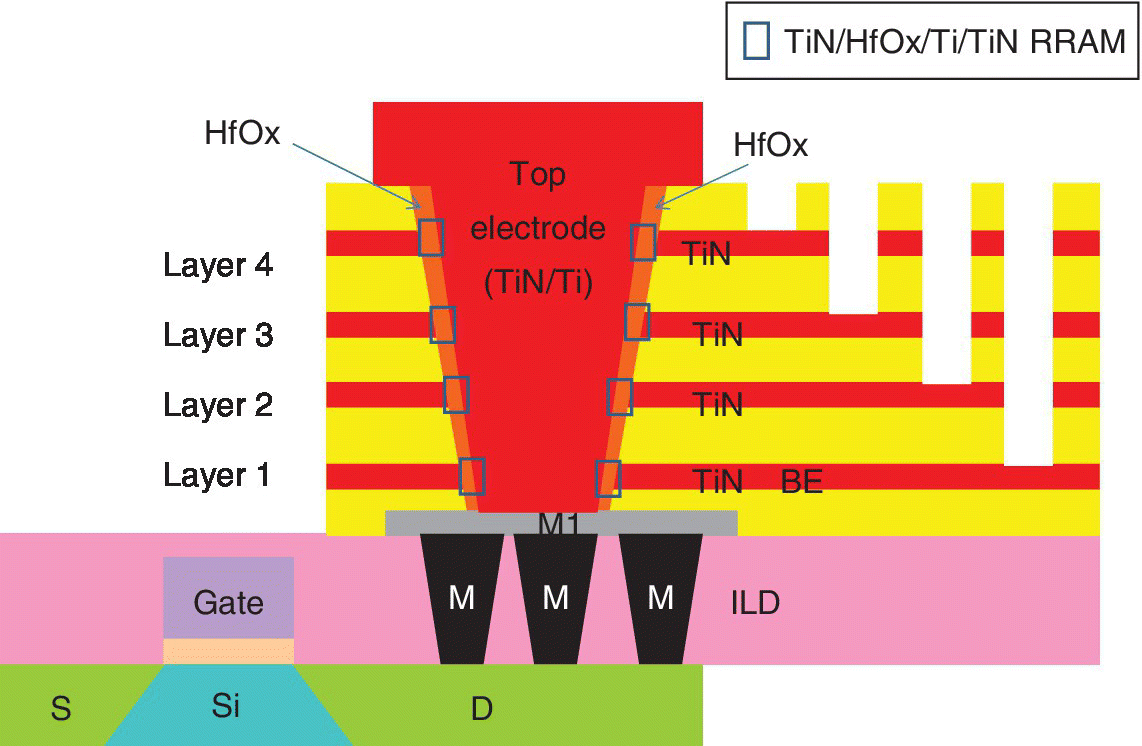
Figure 5.13 Schematic cross‐section of 3D vertical RRAM integrated with FinFET.
Based on H. Li et al. (Stanford University, NNDL Narlabs), VLSI, June 2016 [18].
The 3D architecture was intended for dense neuron‐in‐memory computing and implemented 1011 address and read cycles on 3D RRAM. The RRAM stack was used as a 3D neuromorphic vision system based on a 32 × 32 × 4 3D array. The input and output neurons were connected by the 3D RRAMs acting as 3D variable resistance synapses. A winner‐take‐all network with a stochastic learning rule was simulated for orientation detection. Four‐layer synapses were self‐organized into distinct resistance maps. The balanced array configuration and unique common pillar structure made this vertical 3D RRAM an energy efficient versatile computing unit.
A manufacturable two‐layer 3D implementation of a metal oxide RRAM crossbar array circuit was described in 2016 by the University of California, Santa Barbara, which could be used for both high density nonvolatile memory applications and also for neuromorphic implementations [19]. Analog timing of the memory state combined with high integration density of resistive RAM was required for compact implementation of a synapse. These are the most frequently encountered devices in artificial neural networks and would be essential for low energy implementations of large scale neuromorphic circuits. One method of increasing the effective RRAM density is by vertical monolithic integration of RRAM crossbar circuits. A bilayer stacked metal oxide RRAM crossbar circuit was fabricated and characterized.
These stacked crossbar arrays can be made using 1T1R configurations, but these three terminal devices have low scalability. The alternative is to use RRAMs without a selector device, which have highly nonlinear I–V characteristics to avoid sneak paths and half select issues. Experimental results showed good uniformity for the RRAMs in both crossbar layers. The process flow used was low temperature and CMOS compatible and could be extended to multilayer stacking.
Another issue is thermal crosstalk, which determines the high maximum temperature of switching. This was estimated to be >700 K for MO‐RRAMs. This means the switching in the bottom device could cause disturbances in the devices stacked above. More needs to be understood about device behavior through the entire crossbar system to know if successful analog computing applications are feasible.
The 3D configuration used in this device monolithically integrated two TiOx ‐based passive crossbar arrays. The fabrication method required no high temperature processing, showed no thermal crosstalk, and could be repeated with additional layers. In this process, two fully passive TiO 10 × 10 RRAM crossbars were monolithically integrated using an in‐situ low temperature reactive sputtering deposition followed by a planarization step. The middle electrodes were shared between the bottom and top layers, as shown in the cross‐section of the process in Figure 5.14. The metal layers were deposited as a blanket using reactive sputtering along with highly selective hard masks such as Al2O3. The hard mask was patterned and the metal etched using an Ar ion beam. The metal feature shape was controlled using tilted etching. Chemical mechanical polishing and etch‐back was used. The maximum temperature during fabrication was 175 °C during sacrificial SiO2 deposition, which permits this crossbar array to be made in the back‐end‐of‐the line (BEOL) over a conventional CMOS process.
Figure 5.14 Monolithic integration of RRAM crossbars with shared middle electrodes.
Based on G.C. Adam et al. (UC Santa Barbara), ESSDERC, September 2016 [19].
Electrical characterization showed good uniformity and analog programmability for the 3D crossbar circuits. The devices were formed using a floating biasing configuration and quasi‐DC current ramps without external or internal compliance. The devices were formed one by one and then immediately switched to the low conductive state. The bottom devices were done first followed by the top layer devices. Bottom devices have an average forming voltage of 2.5 V and top devices 2 V. No thermal crosstalk was seen during forming. Good similarity in device behavior between bottom and top devices was observed.
An ON/OFF current ratio of 10 was observed with a RESET voltage of –1.8 V and SET current of 300 μA. At a RESET voltage of –2.4 V the ON/OFF ratio was about 100. A 74% planarization yield was achieved across the wafer. This work was expected to be a key step toward multilayer RRAM crossbars integrated on CMOS for neuromorphic applications.
5.4 Modeling and Characterization of RRAMs as Synaptic Devices
Since different switchable nonvolatile memory devices can be used as variable synaptic devices in neuromorphic computing, it would be useful to have a test to identify such devices. In 2015, the University of Southampton and the Imperial College, London, described an algorithm intended to identify switchable RRAM devices. These are defined as devices that can be programmed in distinct resistive states and change their state predictably and repeatedly in response to input stimuli [20]. Since RRAM devices can be highly nonlinear, they are useful for applications such as neuromorphic computing. Devices were identified that switch between highly distinct resistive states such as a low resistive state and a high resistive state when subjected to a given biasing protocol. No assumption was made about definition of levels of resistance as “1”s and “0”s. This method extrapolates the statistical significance of difference between two distinct resistive states. These states are measured from devices subjected to standardized bias protocols. A typical testing procedure is illustrated in Figure 5.15.

Figure 5.15 A typical testing procedure for RRAM devices that switch between highly distinct resistive states.
Based on I. Gupta et al. (University of Southampton, Imperial College, London), IEEE Trans. on Circulation and Systems, July 2015 [20].
Modeling, characterization, and optimization of an oxide‐based analog RRAM synapse was discussed in 2016 by Tsinghua and Peking Universities and Southern University of Science and Technology [21]. Such RRAM‐based neural networks have the advantages of low energy consumption, fast computing speed, and low fabrication cost in addition to nonvolatile storage characteristics. Multilevel switching behavior, however, is not easy to control in filamentary RRAM, particularly in the SET process where devices tend to show abrupt switching, which blocks the implementation of on‐line training. Nonfilamentary RRAM devices are possible, but analog synapses tend to have reliability issues. A simulated electric potential is shown in Figure 5.16 (a) for a filamentary device and (b) for a nonfilamentary type device. A voltage drop can be observed in the filament gap region.
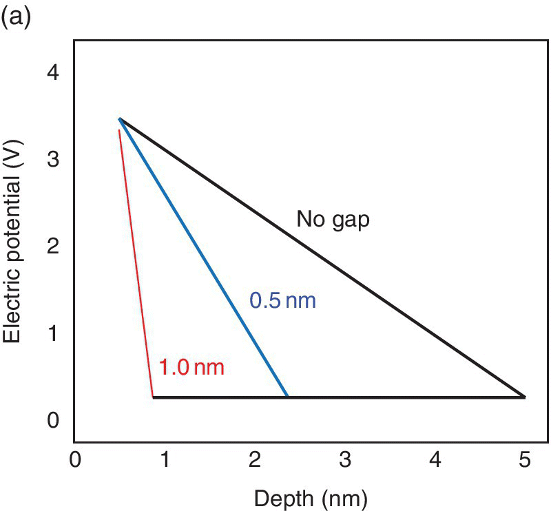
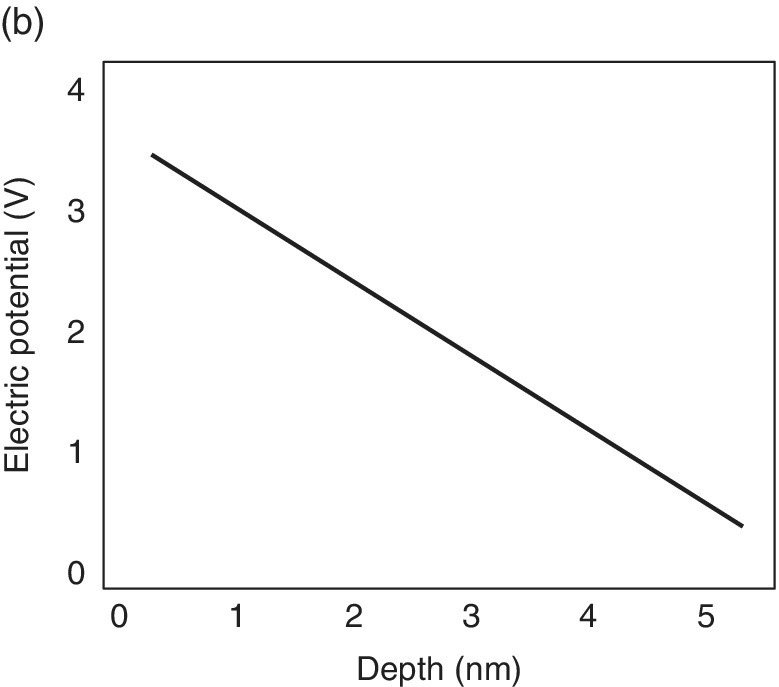
Figure 5.16 Simulated potential for different types of RRAM devices: (a) filamentary showing electric potential drop with increasing gap and (b) nonfilamentary RRAM device.
Based on B. Gao et al. (Tsinghua University, Peking University, Southern University of Science and Technology), IEDM, December 2016 [21].
This experiment develops a physical model based on oxygen vacancy migration to describe the analog switching behavior of nonfilamentary RRAM devices. Simulation analysis results in an optimization method to achieve on‐line training in an oxide‐based analog synapse where a thin oxide switching layer is formed between the electrode or oxygen vacancy (Vo) rich layer and another oxide or semiconductor layer.
During SET, oxygen ions migrate from the switching layer to the Vo reservoir layer, while in RESET, the oxygen ions migrate toward the switching layer. The interface barrier Ei between the reservoir layer and switching layer is modeled from the reaction of oxygen with the Vo layer. A model was based on solid‐state defect theory to describe the migration of Vo. The current was calculated using a Poole‐Frenkel emission model. The resulting physical model describes the analog switching behaviors in the oxide‐based synapse. Analog switching and retention loss were correlated with key material parameters. Optimization guidelines were formed for implementing a high performance neural network system with on‐line training ability.
A new physical model was developed to quantify the analog weight modulation behaviors in the oxide‐based analog synapse. The analog SET, RESET, and retention loss processes were simulated and verified experimentally using an HfOx ‐based synapse.
In the oxide‐based analog synapse, a thin oxide switching layer is formed between the electrode or vacancy (Vo) reservoir layer, and another oxide or semiconductor layer. The device resistance is determined by the concentration of Vo in the switching layer. During SET, oxygen ions migrate from the switching layer to the Vo reservoir layer, while, in the RESET process, the oxygen ions migrated from the Vo reservoir to the switching layer.
It is difficult for the ion drift diffusion model to describe the Vo migration during analog switching due to the nonlinear effect and the large concentration of Vo. A new model was developed based on the basic solid‐state defect theory to quantify the migration of Vo. The current was calculated using a modified Poole‐Frenkel emission model.
An HfO x /SiO y ‐based analog synapse was made. An HfSiO switching layer was shown to form at the HfO2–Si interface with a 4 nm thickness. The resulting I–V curve showed good analog switching in both SET and RESET processes. The resistance was between 107 and 108 ohms, which is higher than filamentary RRAMs. A schematic flowchart for the simulation of analog switching is shown in Figure 5.17.
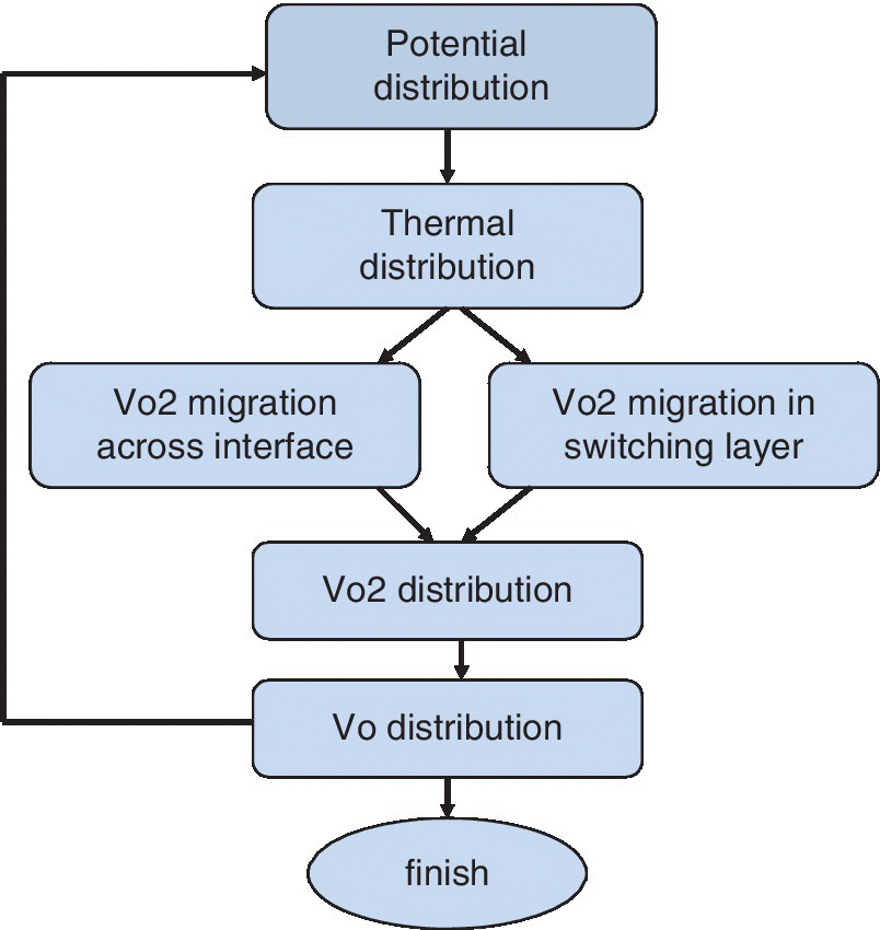
Figure 5.17 Schematic flowchart for simulation of analog switching in an oxide‐based nonfilamentary RRAM.
Based on B. Gao et al. (Tsinghua University, Peking University, Southern University of Science and Technology), IEDM, December 2016 [21].
Analog switching and retention loss were correlated with key material parameters and captured and verified with experiments. Optimization guidelines were provided for boosting the performance and on‐line training ability of the neural network.
5.5 Spiking Neural Nets, STDP, Potentiation, and Depression
5.5.1 Introduction to Spiking Neural Networks
Neuromorphic computing can be achieved using variable resistance memories as synapses in spiking neural networks. Each synapse can have its own conductance profile and these profiles can be altered during evolution of the system. A synaptic array can be configured using self‐rectifying multivalued RRAMs. It can also be configured as a hybrid CMOS/RRAM array using diodes or transistors to eliminate sneak current with multivalued RRAM.
5.5.2 Hybrid RRAM/CMOS STDP Neuromorphic Systems
Resistive memory devices can be used as synapses in neuromorphic cognitive systems. Hybrid MO‐RRAM/CMOS synapses can be based on resistive RAM and transistor circuit design and operation. Real time spike‐based learning and recognition of visual patterns was demonstrated in 2016 by the Politecnico di Milano and IU.NET [22]. The learning accuracy and power consumption of the synapse blocks was discussed. Resistive memories have high speed and small cell size due to the two‐terminal structure and they have high endurance. Hybrid RRAM/CMOS synapses for neuromorphic circuits were shown capable of on‐line pattern learning and recognition. Synaptic schemes can be based on 2T1R and 1T1R structures. The spike‐timing dependent plasticity (STDP) characteristics of the 1T1R synapse with bipolar RRAM was shown along with unsupervised learning with a fully connected neuromorphic network using simulations. Learning efficiency and power consumption of the synaptic blocks was shown.
Hybrid RRAM/CMOS synapses were used in the circuit design, operation, and demonstration of real time spike‐based learning and recognition of visual patterns. The learning accuracy and power consumption of the synapse blocks was discussed. A main requirement of synaptic circuits is being able to tune their resistance in response to incoming neuron spikes according to the STDP protocol, which has been observed in biological systems. Circuit diagrams of a 2T1R synapse and a 1T1R synapse are shown in Figure 5.18.

Figure 5.18 Circuit schematics of (a) a 2T1R synapse and (b) a 1T1R synapse.
Based on D. Ielmini et al. (Politecnico di Milano, IU NET), ISCAS, May 2016 [22].
In both of these circuits, the connections with the PRE and POST permit overlaps between spikes, which enable STDP. The resistive element (circle) can be any two‐terminal memory including a unipolar or bipolar RRAM or phase change memory (PCM).
In the 1T1R design, the BE terminal is connected to the POST to sustain both communication and STDP functionalities. A PRE synapse–POST circuit for a 1T1R synapse is shown in Figure 5.19. The PRE spike applied to V g together with a constant bias sustained by the POST at V te excites a transient current in the 1T1R synapse. Figure 5.19 shows this as the negative constant V te, which induces a negative spiking current corresponding to the PRE spike applied to V g. The spiking current enters the POST using the BE and is integrated, causing a staircase‐type increase in the internal potential V int in the POST. As V int exceeds a threshold, the POST delivers a forward spike to the next neuron layer and a backward spike to the V te. The backward spike acts as the STDP function and may have various shapes depending on the various specific RRAM used.

Figure 5.19 Circuit of 1T1R synapse connecting PRE and POST in a spike‐timing dependent plasticity (STDP) integrate and fire network.
Based on D. Ielmini et al. (Politecnico di Milano, IU NET), ISCAS, May 2016 [22] (permission of IEEE).
Waveforms of V g and V te for delta t > 0 and delta t < 0 are shown in Figure 5.20 (a) and (b) respectively. The PRE circuit drives V g, which induces a current spike in the 1T1R, which is integrated by the POST circuit. The membrane potential V int increases by integration, eventually causing a fire event as it exceeds a threshold. At the fire event, a backward POST spike is applied to V te to induce potentiation (depression) in case of overlap with the PRE spike with Δt > 0 (Δt < 0).
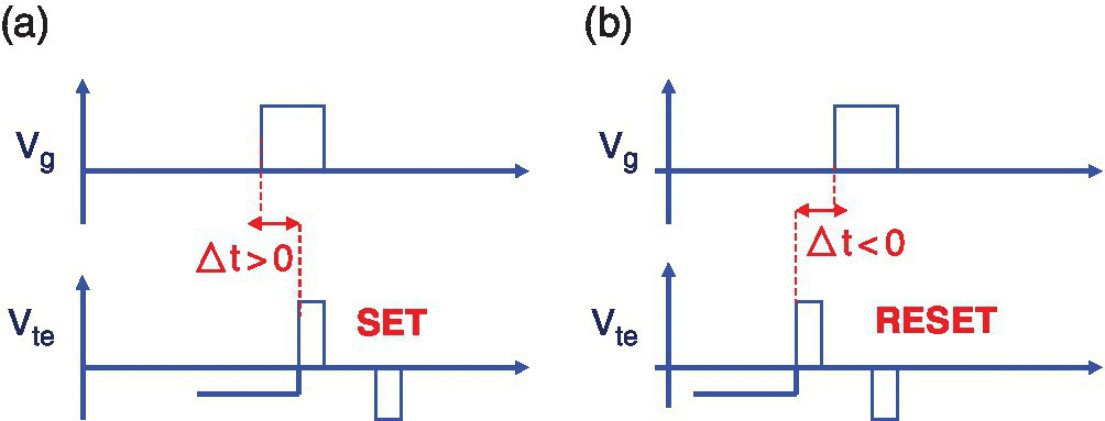
Figure 5.20 Waveforms of V g and V te for (a) potentiation (Δt > 0) and (b) depression (Δt < 0).
Based on D. Ielmini et al. (Politecnico di Milano, IU NET), ISCAS, May 2016 [22] (permission of IEEE).
The results of the analysis supported on‐line pattern learning and recognition by STDP in RRAM‐based synapses. A critical parameter for on‐line learning and recognition is power consumption. It was found that, by reducing the compliance current with filament size, downscaling was possible and that STDP energy could be decreased by reducing the pulse width for potentiation and depression. The compliance current is set to control the resistance value of the low resistance state (LRS) during the SET operation. It was estimated that the energy per synapse during a fire event could be as small as 1 pJ. The communication energy also needed to be reduced, which involved the spike duration. It was found energy could be reduced below the fJ range.
A 1T1R (RRAM) synapse capable of spike‐timing dependent plasticity was discussed in 2016 by the Politecnico di Milano, IU.NET, and Micron. It had an area improvement over the previous 2T1R structure [23,24]. This synapse circuit used a one transistor one RRAM (1T1R) structure as a tunable connection between a presynaptic neuron (PRE) and a postsynaptic neuron (POST). The RRAM synapse passively transmitted spikes and also updated its weight according to a spike‐timing‐dependent plasticity (STDP) protocol. The STDP characteristics were characterized and modeled. A two‐layer neuromorphic network was shown with pattern learning and recognition with deterministic and stochastic switching.
The RRAM device was a silicon‐doped HfO2 layer with a TiN bottom electrode and Ti top electrode. 1T1R devices were used for pulsed demonstration of driving the top electrode and gate nodes using a waveform generator. The RRAM device had a typical bipolar IV curve. It was demonstrated as a 1T1R synapse connected to PRE and POST as Figure 5.21 (a). Typical spike signals at V g and V te are shown in Figure 5.21 (b).

Figure 5.21 1T1R synapse: (a) circuit connected to PRE and POST and (b) typical spike signals.
Based on S. Ambrogio et al. (Politecnico di Milano, Micron Tech.), IEEE Trans. on Electron Devices, April 2016, VLSI, June 2016 [23, 24].
A V g spike from PRE induces a current, which is integrated by POST and eventually leads the synapse to fire. At fire, V te induces potentiation for Δt > 0 or depression for Δt < 0, resulting in STDP.
The STDP characteristics, in this case the change of conductance as a function of Δt, are illustrated in Figure 5.22 and were found from both experiments and calculations. The range of conductances are shown from 25 to 500 kohm. The change of conductance was found for increasing initial resistance R 0.
![Graph of Ro/R vs. delta t [ms] displaying seven curves, with top and bottom curves labeled 500 kOhm and 25 kOhm, respectively.](http://images-20200215.ebookreading.net/2/1/1/9781119296355/9781119296355__memories-for-the__9781119296355__images__c05f022.gif)
Figure 5.22 STDP characteristics: change of conductance versus Δt.
Based on S. Ambrogio et al. (Politecnico di Milano, Micron Tech.), IEEE Trans. on Electron Devices, April 2016, VLSI, June 2016 [23, 24].
A two‐layer neuromorphic network was demonstrated being used with a visual input pattern disturbed by a typical random noise pattern with a typical output pattern and noise sequence appearing at POST. Learning was shown after a given number of cycles.
The 1T1R RRAM synapse capable of spike‐timing‐dependent plasticity was shown to be an area improvement over the earlier 2T1R structure. STDP functionality was shown along with robust learning by deterministic and stochastic synapses. A 103 reduction in power consumption was shown as a result of using a burst operation. The RRAM was based on a silicon‐doped HfO2 layer with a TiN bottom electrode and Ti top electrode.
Learning and classification of handwritten digits from the MNIST database was simulated. A fully connected two‐layer perceptron network for simultaneous multipattern learning of 10 digits was used with a second layer consisting of 10 neurons interconnected by an inhibitory synapse permitting differentiating learning of multiple digits. The first layer had 784 neurons and the second had 10. The MNIST handwriting digit classification showed 86% efficiency.
An RRAM‐based neuromorphic computing device with a 1T1R crosspoint array was described in 2015 by Tsinghua University [25]. The 1T1R array is shown in Figure 5.23. The 1T1R crossbar array minimized the sneak paths of the 1R and 1R1S array and was shown to have lower power dissipation than a 1R RRAM neuromorphic computing device.
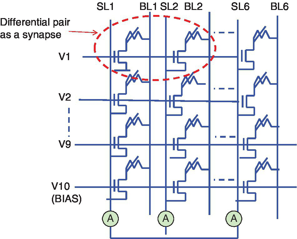
Figure 5.23 Circuit diagram using RRAM 1T1R crossbar array, which eliminates sneak paths. A differential pair is used as a synapse as illustrated.
(Based on P. Yao et al. (Tsinghua University, Tsinghua National Laboratory), NVMTS, October 2015 [25].
Both the two‐terminal 1R and 1S1R crossbar arrays when implemented in a synapse network have good performance but suffer from both sneak path current and program disturb. These limit the computing accuracy of the neural network and also limit the size of the array. In this study, a 1T1R cell is used as the element for an optimized synapse array for neuromorphic computing. A differential pair formed a synapse. Pattern classification was done by simulation using this architecture and the impact of RRAM cell variation on the system was analyzed.
In a column the top electrode of the RRAM is connected to the BL and the source of the transistor is connected to the SL. In a single row, all cells have their transistor gate connected to the same word‐line. This organization decreases the sneak current significantly both suppressing disturbance and decreasing power consumption.
In the proposed neural network, a single layer was used based on a 10 × 6 1T1R synapse array. An RRAM model with asymmetric bipolar switching performance was used. Six columns were divided into three classes in accordance with three output neurons. Every two columns in sequence together connect to a post‐neuron. The difference current is the current that flows to the first output neuron. The schematic of the single‐layer bipolar neuron network is shown in Figure 5.24.
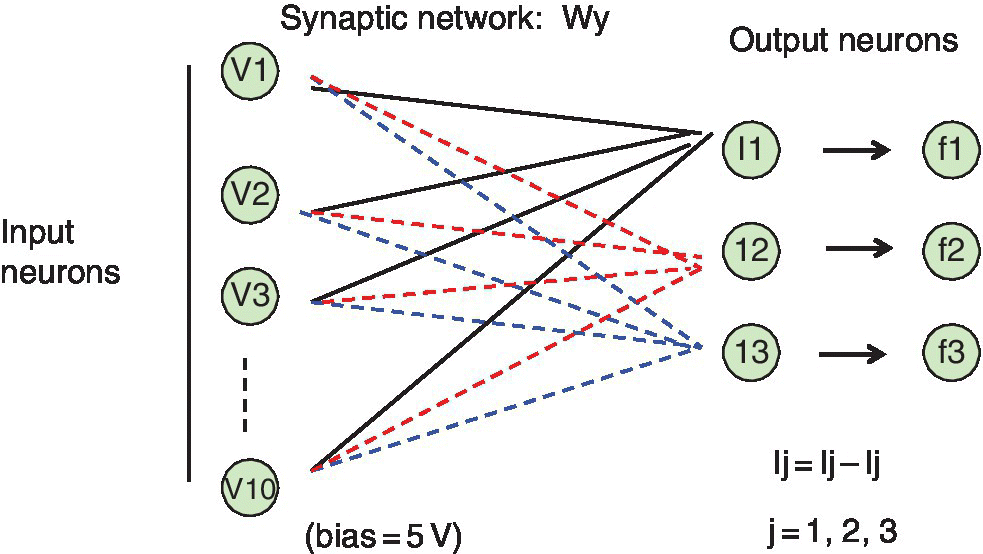
Figure 5.24 Schematic of single‐layer bipolar neuron network.
Based on P. Yao et al. (Tsinghua University, Tsinghua National Laboratory), NVMTS, October 2015 [25] (permission of IEEE).
A total of 30 synaptic weights is realized as two synapse cells representing a synaptic connection. The 10 × 6 1T1R synaptic array connects with three post‐neurons and 10 inputs, which include a constant bias input. Ten training patterns are input as a 3 × 3 pixel black and white image and the input signal is represented by a gate voltage of 5 or 0 V, corresponding to a black or white pixel. All the 1T1R are HRS initially (dark block). After the pattern is applied, the whole array is at read mode simultaneously. To adjust each cell’s weight a parallel programming operation strategy is used column by column where the SET and RESET process are separated. After 15 interations, the final distribution in each column, shown in Figure 5.25, is the input letters “z”, “v” and “n”.
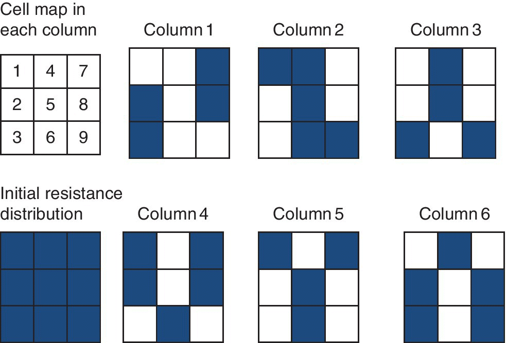
Figure 5.25 The final resistance distribution of each column.
Based on P. Yao et al. (Tsinghua University, Tsinghua National Laboratory), NVMTS, October 2015 [25].
Compared with the same function done with a 1R‐based RRAM crossbar array, the new 1T1R synapse architecture operates more easily and converges more rapidly. The 1T1R structure has low power consumption and the parallel operating mode decreases power dissipation further. The resulting power dissipation was about half that of a 1R RRAM array.
5.5.3 Memory Synapse and Neuron Systems
An oxide‐based analog synapse device and an insulator–metal transition (IMT) oscillator neuron device were described for a neuromorphic system in 2016 by POSTECH [26]. The redox reaction was controlled at the metal/PrCaMnO3 (PCMO) interface of the synapse device in order to control synapse characteristics such as switching uniformity, disturbance, retention, and multilevel data storage under identical pulse conditions. For the neuron device, an Mo electrode was shown to have the best data retention characteristics. Using the IMT characteristics of NbO2 film, an IMT oscillator was developed for the neuron. Accurate pattern recognition was found using the Mo/PCMO synapse array and the NbO2 oscillator neuron.
The required parameters of the synapse device defined by the ITRS roadmap for semiconductors of 2013 included: energy consumption of <10 fJ, operating speed of > 10 Hz, endurance of 109, 32 states (5‐bits), and data retention of 10 years. Also required were: analog conductance change, constant rate of change in conductance, symmetric conductance increase and decrease, and a high density 3D fabricated array.
For the Mo/PCMO device, it was found that the conductance is proportional to the device area so scaling could reduce the switching power. The potentiation and depression characteristics of the Mo/PCMO devices under identical pulse with varying voltage amplitude of pulse were shown to exhibit a gradual conductance change. The change of conductance with increasing voltage amplitude is illustrated in Figure 5.26.
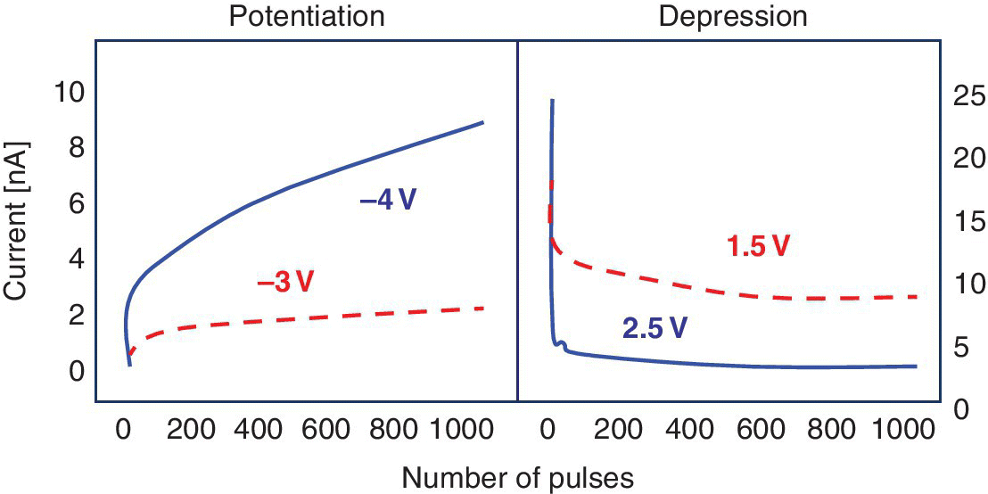
Figure 5.26 Illustration of potentiation and depression characteristics of Mo/PCMO.
Based on K. Moon (POSTECH), VLSI‐TSA, April 2016 [26].
The IMT oscillator neuron using NbO2 had threshold shifting I–V characteristics as shown in the I–V curve in Figure 5.27.
![Graph of current [mA] vs. voltage [V] displaying an ascending curve with circle marker and down arrow for Ron (–1.9 kOhm) and two perpendicular lines with circle marker at the vertex and upward arrow for Roff- 15kOhm.](http://images-20200215.ebookreading.net/2/1/1/9781119296355/9781119296355__memories-for-the__9781119296355__images__c05f027.gif)
Figure 5.27 NbO2 IMT oscillator neuron threshold shifting I–V characteristics.
Based on K. Moon (POSTECH), VLSI‐TSA, April 2016 [26].
When the IMT oscillator neuron was observed above the critical threshold voltage of about 1.3 V the oscillator characteristics were as shown in Figure 5.28. The pattern recognition capability of the Mo/PCMO synapse device with an NbO2 IMT oscillator neuron was tested with a slightly noisy input pattern and the original pattern could be recovered.
![Oscillator characteristics of IMT neuron with square wave for Synapse linked to Neuron (top) and a graph of time (μs) for current [mA] and [uA] depicted by 2 curves with triangular waveform at the middle (bottom).](http://images-20200215.ebookreading.net/2/1/1/9781119296355/9781119296355__memories-for-the__9781119296355__images__c05f028.gif)
Figure 5.28 Oscillator characteristics of IMT neuron with varying bias conditions. Oscillations above the 1.3 V critical threshold voltage are shown.
Based on K. Moon (POSTECH), VLSI‐TSA, April 2016 [26].
Spike‐timing dependent plasticity (STDP) in conductive bridge RAM (CBRAM) devices with silicon neurons was discussed in 2016 by Arizona State University [27]. STDP is a neural process that lets biological neural networks learn by strengthening or weakening synaptic connections between neurons. This research showed the potential for using the on‐state resistance of a CBRAM according to the biological STDP rule for neuromorphic applications. The CBRAM devices were integrated with CMOS spiking neuron circuitry using back end of the line (BEOL) post‐processing. Different initial resistance values and spike durations were used.
To reduce the large power consumption and low density of traditional CMOS‐based implementations, a hybrid neuromorphic architecture was used, which consisted of analog CMOS spike‐generating circuits communicating in a massively parallel architecture using nonvolatile resistive memory devices that can mimic biological synapses. Synaptic plasticity is the ability of biological synaptic connections to be strengthened or weakened as a response to spiking activities of neurons. STDP is a neuronal learning mechanism that involves the dependence of change in synaptic connection strength based on the relative timing difference in arrival of voltage spikes generated by the neurons at the synapses.
Before CBRAMs could be used as electronic synapses, it was necessary to show that the conductance of the CBRAMs could be tuned for use with the STDP rule. On‐chip STDP behavior was shown in CBRAM devices made in the back end of the line (BEOL) on top of a chip containing a CMOS “integrate and fire” neuron circuit. Experimental evidence of true analog STDP behavior in CBRAM was shown that is similar to the biological STDP learning rule. A CBRAM compact model was used to show STDP behavior and how this behavior could be used for applications such as associative memory.
The CBRAM devices were made as a vertical stack of Ag/GeSe on top of metal pads on the chip containing the CMOS neuron circuits. Two CMOS neurons on the chip were connected using a BEOL CBRAM device. Spikes generated at the nodes of the two neurons were applied across the CBRAM device. To demonstrate STDP learning, a relative timing difference was created between the pre‐ and post‐neuron spikes. The test setup to demonstrate STDP with CMOS neurons connected using a single CBRAM synapse fabricated on chip is shown in Figure 5.29.
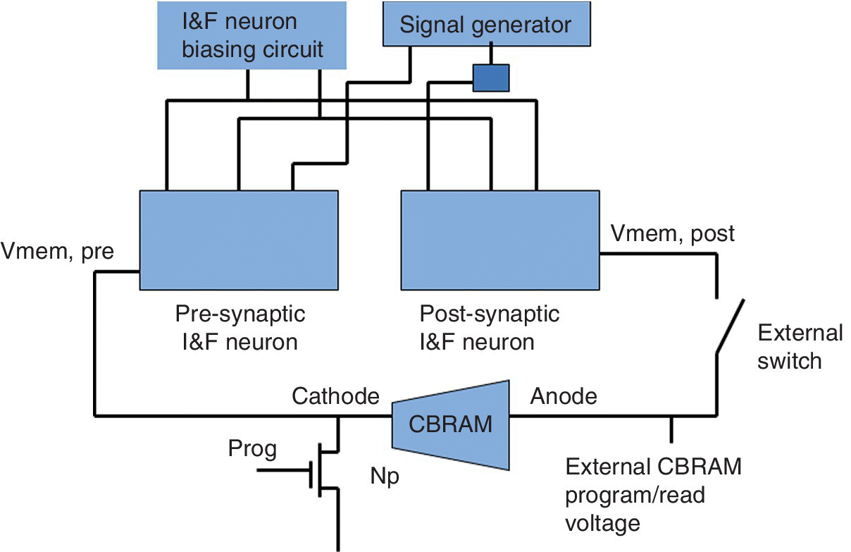
Figure 5.29 STDP demonstration with CMOS neurons connected using a single CBRAM synapse.
Based on D. Mahalanabic et al. (Arizona State University), ISCAS, May 2016 [27].
The chart in Figure 5.30 illustrates the experimentally measured STDP behavior with an on‐chip CBRAM device showing the change in the CBRAM conductance versus spike timing difference for different initial LRS values and a neuron spike width of 7 µs. Experimental results from the die showed an STDP‐based analog resistance change behavior in CBRAM devices that follows the biologic STDP learning function.
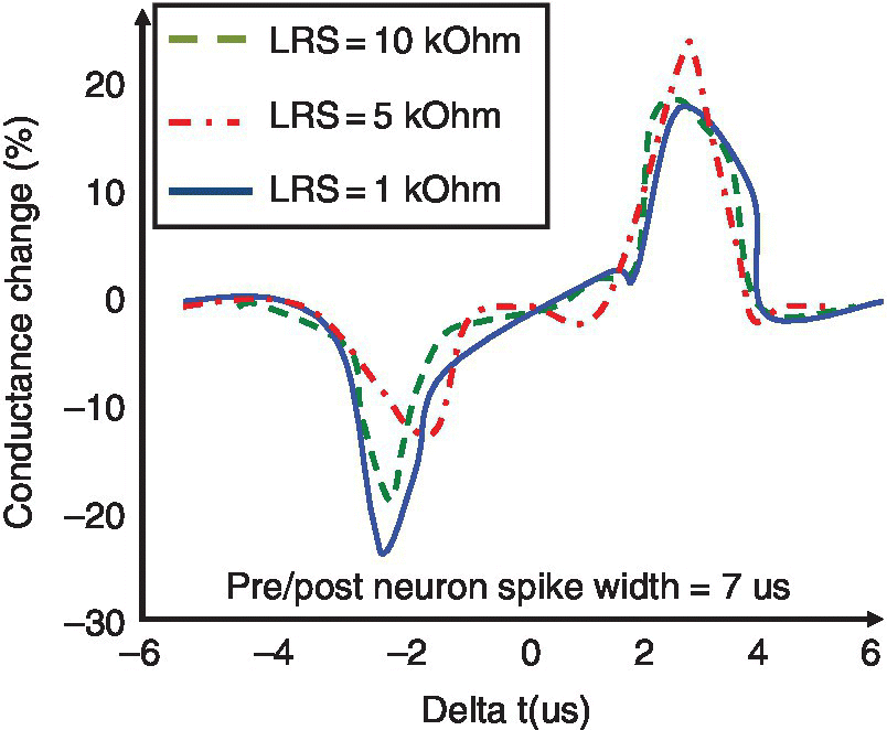
Figure 5.30 Change in CBRAM conductance versus spike timing difference with on‐chip CBRAM.
Based on D. Mahalanabic et al. (Arizona State University), ISCAS, May 2016 [27].
5.5.4 Novel RRAM Synapse Applications
The use of RRAMs in neuromorphic systems was discussed in 2014 by CEA‐LETI [5]. They showed large‐scale energy efficient neuromorphic systems based on RRAM used as stochastic binary synapses. Prototype applications were examined, such as a complex of RRAM memories in neuromorphic circuits for saving energy and increasing performance. They examined visual and auditory pattern extraction using feedforward spiking neural networks. In attempting to imitate the brain, they noted that there are 100 billion neurons in our brain and each of these neurons can have as many as 10 thousand connections to other neurons.
Various neuromorphic systems were studied. An unsupervised neuromorphic system was developed based on GeS2/Ag CBRAM devices, which were programmed as binary synapses with a stochastic STDP learning rule optimized by a genetic evolution algorithm. Two applications were shown including: read time auditory pattern extraction and visual pattern extractions. Highly accurate audio pattern sensitivity was shown. Figure 5.31 shows the architecture for handwritten digits recognition.
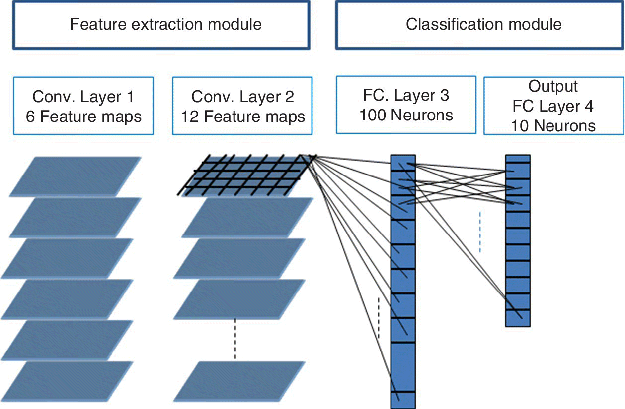
Figure 5.31 Architecture for handwritten digits recognition.
Based on B. DeSalvo et al. (CEA LETI), IMW, May 2015 [5].
A video detection rate greater than 95% and low synaptic power dissipation in the learning mode were shown. In another implementation, a spike‐based hardware convolutional neural network using HfO2 type OxRAM was developed. Multiple binary OxRAM devices in parallel configurations were used to obtain multilevel synapses. A visual pattern recognition application, the identification of handwritten patterns as digits, was described. The architecture was inspired from the mammalian visual cortex, which is composed of two cascaded convolutional layers to associate the extracted feature maps to the 10 digit categories.
A TiO x ‐based RRAM for neuromorphic synapse applications with 64 levels of conductance states due to an optimized interface between the metal electrodes and the TiO x film was discussed in 2016 by POSTECH [28]. To compensate for the change in switching power with increasing pulse number, the use of fixed voltage pulses in potentiation and of fixed current pulses during depression was tried. By adopting a hybrid pulse scheme, the symmetry of conductance change was shown to be significantly improved under both potentiation and depression conditions.
The improved conductance levels and the symmetry of conductance change were directly related to enhance pattern recognition accuracy, which was confirmed by a neural network simulation. A comparison of the voltage and current pulse modes during depression and evolution of the current pulse programming power with pulse number is shown in Figure 5.32. The power increases gradually.
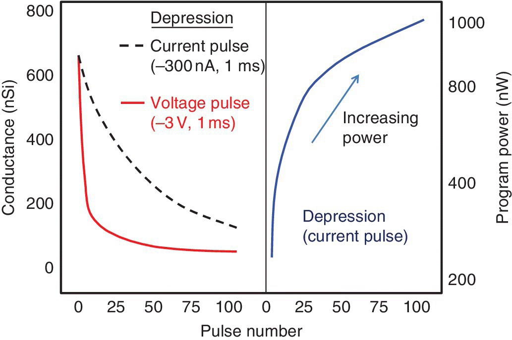
Figure 5.32 Comparison of voltage and current pulse modes for current pulse program power showing conductance in siemens.
Based on J. Park et al. (Pohang University), IEEE Electron Device Letters, December 2016 [28].
An Mo/TiO x ‐based interface RRAM was developed using a hybrid pulse mode for synaptic applications. An interface switching device with 64 conductance levels was obtained by optimizing the redox reaction at the Mo/TiO x stack. The hybrid voltage and current pulse method significantly improved the symmetry of the conductance change in both potentiation and depression, resulting in an improved pattern recognition accuracy.
Short and long term synaptic plasticity using OxRAM with noisy input data was discussed in 2016 by various French laboratories [29]. A new circuit architecture and a read/program strategy to emulate short and long term plasticity rules using OxRAM cells were discussed. The intrinsic OxRAM device switching probability at ultralow power is used to implement short term plasticity (STP) and long term plasticity (LTP) learning rules. The computational power showed that STP provided for reliable signal detection with noisy input data.
Biological synapses show both short term plasticity (STP) and long term plasticity (LTP). LTP results in stable changes of the synapses according to the timing of pre‐ and post‐synaptic spike events. STP can induce dramatic changes in synaptic weights, which enhances the discrimination ability of single neurons even though LTP characteristics have been the primary research objective of neuromorphic research. The co‐implementation of both LTP and STP with the same OxRAM technology is shown.
The emulation of LTP using Ti/HfO2 OxRAMs cells was demonstrated. In this study, the same technology is used for emulating STP. The programming strategy is to reproduce STP using an OxRAM‐based synapse. The method involves having a synaptic weight decreased at each presynaptic spike, which periodically increased with every time interval in the absence of spikes.
The principal circuit that is used to reproduce both STP and LTP rules using nonvolatile OxRAM cells is shown in Figure 5.33. The conductance multiplication during the read operation is done using a buffer, Y(t), which modulates the read voltage for the LTP synapse Sij between the pre‐synaptic neuron (i) and the post‐synaptic neuron (j).

Figure 5.33 Principal circuit used to reproduce STP and LTP rules for an OxRAM cell. The circuit imitates the synapse between neuron (i) and neuron (j). Buffer Y(t) modifies the synapse for either STP or LTP rules.
Based on T. Werner et al. (CEA, LETI, MINATEC, CEA, LIST, INSERM), IEDM, December 2016 [29].
Long and short term plasticity learning rules are derived for reliable unsupervised learning in spiking neural networks with highly noisy input data. It was shown that the STP permits decreasing the false positives by 40% while maintaining a detection rate of 89% for a neural detection application and a low signal‐to‐noise ratio of 3.7.
5.6 Neural Network Systems Using Ferroelectric RAM Technology
5.6.1 Neural Network Circuits Using Ferroelectric Memory (FeMEM) Synapses
In June of 2013 Panasonic discussed on‐chip pattern recognition in a neural network circuit using an NVM [30]. The synapse chip of the neural network consisted of a stack of CMOS circuits and three terminal ferroelectric memristors. The analog and nonvolatile conductance range of the 3 T‐FeMEM was used as a synaptic weight to learn the matrix patterns. The original pattern can be recognized from even an incomplete pattern. A schematic cross‐section of the CMOS circuit and 3 T FeMEM is shown Figure 5.34.
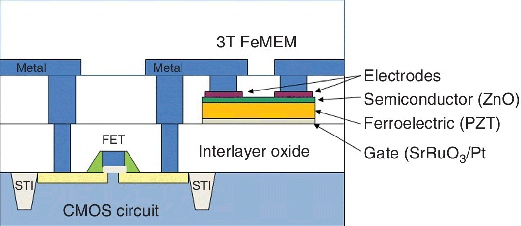
Figure 5.34 Schematic cross‐section of CMOS circuit and 3T FeMEM.
Based on Y. Kaneko et al. (Panasonic), VLSI Technology Symposium, June 2013 [30].
Neural network circuits can effectively provide low power parallel flexible systems for learning and cognitive recognition. A synapse in which the connection weight is modified by learning controls the electrical signals between neurons. This means that continuous conductance modification is required for a biological synapse. In this case, multiple three‐terminal ferroelectric memristors are used as synapses for learning since a gate electrode can control the conductance between the other two electrodes for concurrent learning. The synaptic weight change of a 3 T‐FeMEM is shown in Figure 5.35 as a function of the relative timing of the pre‐ and post‐spikes. The spike width of V post was 5 µs. It is similar to the synaptic weight change of a biological synapse.

Figure 5.35 Synaptic weight change of 3T‐FeMEM versus relative timing of pre/post‐spikes with spike width of V post at 5 µs.
Based on Y. Kaneko et al. (Panasonic), VLSI Technology Symposium, June 2013 [30].
5.6.2 Using the FeMEM in Neural Network Circuits
A neural network circuit was developed that included 9 neurons and 144 synapses using the CMOS circuits and 3 T‐FeMEMs. Learning and pattern recall were demonstrated on this neural network chip.
Fabrication of the 3 T‐FeMEMs was described in 2014 by Panasonic along with the procedure for integrating the 3 T‐FeMEMS into a conventional CMOS circuit [31]. The 3 T‐FeMEM circuit had a back‐gate thin film transistor structure with a stack of ZnO/Pb(Zr,Ti)O3 (PZT)/SrRuO3 oxide on a Pt (111) layer. The Pt layer permitted an oriented ferroelectric PZT film. PZT film polarization control was done using the gate voltage, which modulated the channel conductance nonvolatility.
The synapse function, which consisted of continuous control of the analog conductance of the memory, was done by applying pulse gate voltages. In the “integrate and fire” neuron network, the neurons communicate with each other using voltage pulses. An input voltage pulse from another neuron generates a current pulse with amplitude that is proportional to the synapse conductance. These current pulses are then integrated in a leaky integrator. When the integrated voltage reaches a threshold, the pulses are output to other neurons through their synapses and are fed back to the former synapses. All neurons operate simultaneously, resulting in parallel computation.
The two‐neuron circuit connected by a synapse composed of the 3 T‐FeMEM and a selector is shown in Figure 5.36. A neuron outputs a single rectangle pulse and a triple rectangle pulse to the following synapse. The single rectangle pulse is also fed back to the initial synapse.
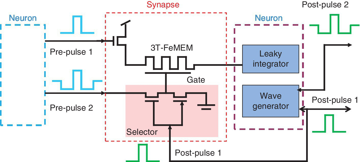
Figure 5.36 Two neuron circuit connected by a synapse containing a 3T‐FeMEM and a selector. The first neuron outputs to the synapse a single rectangle pulse to the 3T‐FeMEM and a triple rectangle pulse to the selector. The single rectangle pulse is fed back to the synapse as post‐pulse 1.
Based on Y. Nishitani et al. (Panasonic), DRC, June 2014 [31] (permission of IEEE).
Recall was demonstrated by inputting a gray pattern. The recalled pattern approached the learned pattern as the recall proceeded. It was concluded that the synapse chip with 3 T‐FeMEM is suitable for use as an artificial electronic synapse.
In August of 2014, Panasonic discussed ferroelectric artificial synapses, which were used in a spiking neural network for recognition of a multishaded image [32]. This pattern recognition is based on a spiking neural network model using 3 T‐FeMEMs as synapses. This synapse chip is formed by stacking CMOS circuits and 3 T‐FeMEMs. The conductance of the 3 T‐FeMEM is gradually changed by varying the amplitude of the applied voltage pulse. The analog and nonvolatile conductance change of the 3 T‐FeMEM is used as a synaptic weight. When an incomplete multishaded pattern is input to the neural network circuit, it automatically completes and recalls a previously learned pattern.
The 3 T‐FeRAM is used as a synapse to demonstrate on‐chip pattern recognition in a neural network circuit with multiple neurons based on a spiking neural network model. The three‐terminal structure offers the advantage of a simple learning scheme. The three‐terminal device is capable of realizing signal transmission and synapse learning concurrently in synapse connected neuron pairs.
5.6.3 Ferroelectric Tunnel Junctions in Neuromorphic Circuits
In February of 2014, a ferroelectric tunnel junction (FTJ) was used to simulate a spike‐timing dependent plasticity circuit for use in neuromorphic circuits [33]. Memristive behavior has been observed in ferroelectric tunnel junctions. In a conventional FTJ with an ultrathin ferroelectric barrier of <5 nm, tunnel resistance can be changed between ON and OFF states by switching the ferroelectric polarization. It has been shown that the change of resistance can occur continuously rather than abruptly, which defines a ferroelectric tunnel memristor (FTM). An FTM shows large OFF/ON resistance ratios and high operation speed, which is promising for use in multilevel memories and synapsis‐like circuits.
The ferroelectric tunnel memristor has resistance that can be continuously tuned by controlling the growth of domain in the ferroelectric tunnel barrier. It has an OFF/ON resistance ratio >100, high operating speed of 10 ns, multilevel storage, and neuromorphic circuits. A compact model was developed for a voltage controlled FTM based on experimental results and ferroelectric switching dynamics. Resistance measurements were taken as a function of the amplitude and duration of programming voltage pulses. Good agreement was found between simulation results and experimental measurement. An FTM‐based spike timing dependent plasticity circuit was simulated to show its use in neuromorphic circuits. If a programming voltage was applied to the ferroelectric film with a fully up‐polarized domain, the down‐polarized domains nucleate and propagate and the tunnel resistance can be calculated by the parallel resistance model.
A typical neuromorphic network for an STDP application is shown in Figure 5.37, based on a 2 × 2 crossbar. The spikes produced by neurons can tune the memristor conductance, which is the synaptic weight. The change of the weight is approximately an exponential function of the time difference between the pre‐spike and post‐spike.
Figure 5.37 Typical neuromorphic network for an STDP application using ferroelectric tunnel memories for synapsis.
Based on Z. Wang et al. (University of Paris‐Sud, Beihang University), Applied Physics Letters, February 2014 [33].
For LTP, a positive voltage pulse whose width decays with the time frame is generated when the pre‐neuron spikes and a negative pulse of constant width is triggered between the top electrode and the bottom electrode when the post‐neuron spikes. For LTD, a positive voltage pulse of decaying width is produced between the top electron and the bottom electrode when the post‐neuron spikes. Meanwhile, a positive pulse of constant width occurs at the MOS gate when the pre‐neuron spikes.
A compact model of the ferroelectric tunnel memristor was based on ferroelectric switching dynamics and experimental results. The model was programmed in Verilog A language for the Cadence platform and Spectre simulator.
Synaptic plasticity can be mimicked by electronic synaptic devices. In January of 2016, ETRI discussed synaptic plasticity in ferroelectric thin film transistors where the channel conductance was gradually modulated by varying the amounts of aligned ferroelectric dipoles [34]. By using ferroelectric thin films as the gate insulator for thin film transistors (TFT), channel conductance can be defined as the synaptic plasticity, and is gradually modulated by variations in the amounts of aligned ferroelectric dipoles. Poly(vinylidene fluoride‐trifluoroethylene) [P(VDF‐TrFE)]‐poly (methyl methacrylate) (PMMA) blended films were chosen and their switching kinetics were investigated. The switching time for ferroelectric polarization was influenced by the amplitude of the applied electric field and the ratio of ferroelectric beta‐phases in P(VDF‐TrFE)‐PMMA films. The switching time of the P(VDF‐TrFE) increases when decreasing the pulse amplitude or the ratio of ferroelectric beta‐phases by including PMMA. The activation electric field was also found to increase with the blended amount of PMMA.
Synapse TFTs were made using the P(VDF‐TrFE)‐PMMA as gate insulator and In‐Ga‐Zn‐O for active channels. The drain currents of the synapse TFTs gradually increased when voltage pulse signals of a given duration were applied repeatedly. This suggested that the synaptic weights could be modulated by the number of external pulse signals and that the proposed synapse TFT could be used to mimic the operation of biosynapses.
5.7 Early Neuromorphic Computers Using Phase Change Memory
A 2‐PCM synapse for use in a large scale neuromorphic STDP system was discussed in 2012 by CEA‐LETI and CEA‐LIST [35]. The neural network architecture used the gradual crystallization behavior of a PCM device to emulate both synaptic potentiation and synaptic depression. They used a simplified biological learning rule where long term potentiation and long term depression can be produced with a single invariant crystallizing pulse.
The architecture was simulated on an event‐based simulator using a behavioral model for the PCM devices, which was validated with electrical characterization. The system was comprised of about 2 million synapses and directly learns from event‐based dynamic vision sensors. It was tested with real data and was able to extract complex and overlapping temporally correlated features such as car trajectories on a freeway. Complete trajectories could be learned with a detection rate above 90%. The synaptic programming power consumption during learning was found to be as low as 100 nW for scaled PCM technology.
An energy efficient 2‐PCM synapse using PCM elements as the synapses in large scale neuromorphic systems was discussed in August of 2012 by CEA‐LIST, CEA‐LETI, and MINATEC [36]. The spiking neural network architecture used the gradual crystallization behavior of the PCM to emulate synaptic potentiation and synaptic depression. A simplified rule was used where long term potentiation and depression can both be products with a single invariant crystallizing pulse. Simulations were run using a behavior model for the PCM devices.
The system of 2 M synapses learned from event‐based dynamic vision sensors and was able to extract complex features such as car trajectories on a roadway. Power consumption was estimated to be as low as 100 nW. Robustness to variability was noted. Previously similar implementations have been published with memristor‐type devices. PCM is, however, considered a promising embedded memory technology for large scale integration in CMOS.
A hardware implementation of brain‐inspired architecture consisting of 2‐D crossbar arrays of phase change synaptic devices was discussed in December of 2013 by Stanford University, the University of Pennsylvania, and IBM [37]. These devices were shown to achieve associative learning and perform pattern recognition. Device and array‐level studies were done using a 10 × 10 array of phase change synaptic devices. These devices exhibited pattern recognition that was robust against synaptic resistance variations. Large variations can be tolerated by increasing the number of training iterations. Measurements showed that an increase in initial variation from 9 to 60% causes required training iterations to increase from 1 to 11.
It was demonstrated that brain‐like pattern recognition could be implemented using 2‐D crossbar arrays of phase change synaptic devices. Individual synaptic device characteristics were presented first for phase change devices in a 10 × 10 array. An example of a single PCM cell DC switching is shown Figure 5.38.
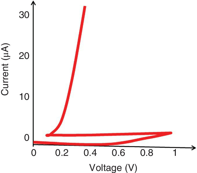
Figure 5.38 Single PCM cell DC switching.
Based on S.B. Eryilmaz et al. (Stanford University, University of Pennsylvania, IBM), IEEE IEDM, December 2013 [37].
The array level operation and programming method and algorithms used for learning were explained. Finally, analysis on resistance variation and its effect on array level learning and pattern completion were discussed. Gradual programming to achieve analog storage was done by applying multiple pulses to the same PCM cell, as illustrated in Figure 5.39. By adjusting pulse amplitudes and widths, it is possible to do more gradual switching.

Figure 5.39 Illustration of gradual SET characteristics of a single cell.
Based on S.B. Eryilmaz et al. (Stanford University, University of Pennsylvania, IBM), IEEE IEDM, December 2013 [37].
The 10 × 10 crossbar array had 100 synaptic devices and 10 recurrently connected neurons. The computer supplied integrated and fire neurons and PCM cells were used as synaptic devices between neurons. The input terminal of each neuron was connected to a bit‐line (BL) node and the output terminal of each neuron was connected to a word‐line (WL) node. In learning, synaptic weights are updated so that synapses between coactive neurons that fire in the same 100 µs time window get stronger; otherwise the synaptic weight does not change.
It was shown that the synaptic networks could implement a robust pattern recognition through brain‐like learning. Test patterns were shown capable of being stored and recalled associatively. Initial resistance variations could be tolerated by adding more training, which consumed more energy.
A 64 K‐bit cell phase change memory (PCM) synaptic array with on‐chip neuron circuits for continuous learning was discussed in 2015 by IBM [38]. The neuromorphic core with a 64 k cell PCM synaptic array had a learning capability. The 256 configurable on‐chip neuron circuits performed leaky integrate‐and‐fire (LIF) and a synaptic weight update based on spike‐timing dependent plasticity (STDP). A 2 T‐1R PCM unit cell separates LIF and synaptic learning paths, minimizing the neuron circuit size. The circuit for the STDP learning algorithm along with a 2 T‐1R structure enables both LID and STDP learning to operate asynchronously and simultaneously within the array. This avoids power consumption associated with timing methods as well as other complications. A hardware demonstration of learning with large capacity due to a large array size and analog synaptic weights was shown.
In the LIF mode circuit, shown in Figure 5.40 (a), when the pre‐synaptic neuron fires, the axon driver enters its LIF mode. The axon driver generates a short LIF pulse on the LIF WE to turn on LIF TR. This discharges the neuron circuit capacitor through the LIF transistor and PCM cell. The neuron circuit fires if the voltage on the capacitor drops below a threshold voltage and then after a short delay triggers the STDP bit line. The leak resistor continuously restore V cap to the resting potential.
In the STDP mode, shown in Figure 5.40 (b), after the AD turns off the LIF transistor, it continues to enable the STDP transistor with a slowly varying STDP pulse on the STDP word‐line. If the neuron circuit generates an STDP bit line pulse while the STDP transistor is on, the PCM cell is programmed. The size of resistance change is determined by the STDP word‐line voltage governed by the relative timing between the STDP WL pulse and the BL pulse.
Figure 5.41 illustrates the RESET current in μA versus SET resistance in ohms for a PCM. The area of applicability to storage class memory and for synaptic memory is indicated on the chart. For a synaptic memory device with power <0.8 pJ, the RESET current must be lower than 40 μA and the SET resistance around 106 ohms.

Figure 5.40 Illustration of neuromorphic circuits in (a) LIF mode and (b) STDP mode.
Based on S. Kim et al. (IBM), IEDM, December 2015 [38] (permission of IEEE).

Figure 5.41 Illustration of the RESET current versus SET resistance for a PCM.
Based on S. Kim et al. (IBM), IEDM, December 2015 [38].
In September of 2015, IBM and the Universities of Oxford and Exeter discussed using PCM with FET access devices [39]. A detailed study of accumulation‐based computation was done and efficient factorization using PCM cells was shown with the intent of this leading to massively parallelized computations. It was shown that CMOS‐integrated PCM cells can be used to perform arithmetic operations using an accumulator‐based computational method. Advanced arithmetic capabilities were shown. Intermediate states between pulses were shown to be accessible for up to an hour, which demonstrates that a phase‐change accumulator can realize a form of non‐von Neumann computing in which the intermediate states of a calculation may be stored simultaneously by the same cell that carries out the computation. Scaling would reduce the power consumption without affecting the computational properties.
The progress in phase change memory in terms of brain‐inspired neuromorphic systems implemented with PCM was discussed in 2016 by IBM and Macronix [40]. The PCM field was surveyed over the previous five years. Two paths towards higher density were discussed. One was through 3D integration using PCM and 3D capable access devices. The other was through using multiple bits per cell while managing resistance drive caused by structural relaxation of the amorphous phase. Brain‐inspired neuromorphic systems using PCM were also described.
5.8 Resistive RAMs in Neuromorphic System Design and Application
5.8.1 Design for Synaptic Devices for Neuromorphic Computing
In June of 2014, ASU, Stanford, and the University of Pennsylvania discussed design considerations for synaptic devices for neuromorphic computing [41]. Two terminal RRAMs with electrically triggered resistance modulation were proposed as synaptic devices for neuromorphic computing. These included phase change memory (PCM), resistive RAM, and CB‐RAM. This study considered design considerations of synaptic devices for plasticity and learning. An ideal synaptic device should have characteristics like: dimension, energy consumption, operation frequency, and dynamic range that are scalable to biological systems with comparable complexity.
The HfOx RRAM is considered a good candidate for large scale integration of a neural network since synaptic devices with scalability to sub‐10 nm are preferred and an HfO x RRAM cell has been demonstrated as 10 nm × 10 nm. The energy consumption per synaptic event is around 1–10 fJ and some HfO x RRAM have already shown sub‐pJ energy consumption. Brain‐like systems can operate as slow as 1–10 Hz, which gives the 10 ns operating RRAM a lot of flexibility to design trade‐offs for energy consumption.
Synaptic plasticity characteristics in biological synapses show analog‐like behavior with many synaptic weight states. In general, multilevel states bring advantages to networking. The RRAM has level programmable RESET. A 10 year data retention is required along with about 109 endurance cycles. A disadvantage of the RRAM and the CB‐RAM is variability in the resistance modulation, which will require further material and device engineering.
Using a RRAM crosspoint array for dictionary learning was discussed in 2014 by Arizona State University [42]. The array had a neurophysics‐inspired parallel architecture, which performed matrix product and dictionary update in a fully parallel fashion at a speed that is independent of the matrix dimension. The system was implemented in 65 nm CMOS technology using an RRAM memory cell for high speed unsupervised dictionary learning. It performed more than 3000 times faster than state‐of‐the‐art software, which enabled real‐time feature extraction on a single chip.
The resistive crosspoint array structure was used since the crosspoint mimics the structural map of a neural system. At each crosspoint, the conductance of a memory cell represents the synapse weight, as shown the graph in Figure 5.42 of conductance change versus voltage pulse width. RRAM is used due to its nonvolatility, high integration density, and low power consumption. Analogous to a synapse device, the conductance of an RRAM cell is increased (decreased) by a positive (negative) voltage pulse.
Figure 5.42 Conductance change as a function of voltage pulse width “t”.
Based on D. Kadetotad et al. (Arizona State University), Biomedical Circuits and Systems Conference, October 2014 [42].
Suppressing intrinsic variations during the synaptic training process in metal‐oxide synaptic RRAMs was discussed in October of 2014 by Peking University [43]. These variations can affect the accuracy of the neuromorphic computations. The influence was investigated of resistance variations on metal‐oxide RRAM‐based neuromorphic computation systems. Atomic DMC (Dynamic Monte‐Carlo) simulations were performed to study the random migration of oxygen vacancies that are responsible for the origin of the variations. A new methodology was suggested to improve the robustness of the metal‐oxide RRAM‐based neuromorphic computation system.
Neuromorphic computing, which has features of parallelism, adaptivity to complex input information, and error tolerance, was discussed by Stanford University in 2015 [44]. The synapse in a neuromorphic system requires high integration density and low energy consumption, which are properties of oxide‐based RRAM. An optimized oxide‐based RRAM synaptic device was designed and applied to the performance of a neuromorphic visual system. The intrinsic variation of the RRAM synaptic devices was suppressed to achieve the high recognition accuracy and efficiency required in a neuromorphic visual system.
5.8.2 Using RRAMs in Various Neuromorphic Computing Applications
Neuromorphic computation is used more effectively than von Neumann systems in applications such as image and auditory processing. In December of 2015, Peking University and Sandisk discussed an optimized learning method for grayscale image recognition in an RRAM‐based analog neuromorphic system [45]. An analog neuromorphic visual system is developed using a fabricated RRAM array as a synapse network. A new training method is used to optimize the performance of the system by using segmented synaptic behavior. This segmented behavior is due to the dynamics of the conductive filament. Initially the CF thins near the top electrode and resistance increases slowly. When the CF is just ruptured the electric field intensity increases due to the small tunneling gap, which results in faster resistance change. As the gap enlarges, the resistance slowly increases with the resistance increase slowing and then finally saturating.
The experimental results using the segmented method indicated that learning accuracy was improved from 77.83 to 91.32% over a nonsegmented system, energy consumption was decreased by more than two orders of magnitude, and learning efficiency improved over traditional learning schemes.
Figure 5.43 shows a neuromorphic system consisting of CMOS neurons and RRAM synapses. In this system the RRAM devices serving as synapses connect the CMOS neurons at the different layers. The conductance of the RRAM synapse represents the strength of the connection between two neurons. This can be modified during the training process by using SET and RESET pulses to change the conductivity of the RRAM.
Figure 5.43 Illustration of neuromorphic system of CMOS neurons and RRAM synapses.
Based on Z. Chen et al. (Peking University, Sandisk), IEDM, December 2015 [45].
In December of 2016, Arizona State University and Tsinghua University discussed using a binary neural network with RRAM synaptic devices for classification and on‐line training [46]. A large scale neural network was made for use in image recognition. The goal was to find a methodology to binarize the neural network parameters with the intent to reduce the precision of weights and neurons to 1‐bit for classification and less than 8‐bit for on‐line training. An experimental binary neural network was demonstrated on Tsinghua’s 16 Mb RRAM macro chip made in 130 nm CMOS. The system performance on the MNIST handwritten digital dataset achieved 96.5% accuracy for both classification and on‐line training and nearly 97% accuracy by ideal software implementation.
5.8.3 Large RRAM Array Design for Neuromorphic Computing
Various issues with designing large RRAM arrays in neuromorphic computing applications were discussed in 2016 by IBM, POSTECH, and EPFL [47]. In these neuromorphic schemes, device conductance serves as a synaptic weight allowing the multiply‐accumulated operation in these algorithms to be performed using the weight data. An illustration of neuromorphic non‐Von Neumann computing is shown in Figure 5.44. Here neurons activate each other through networks of programmable synaptic weights, which can be implemented using dense crossbar arrays of resistive RAMS with variable resistance as 1T1R cells that emulate synapses coupling “neuron”‐controlled selector device pairs.
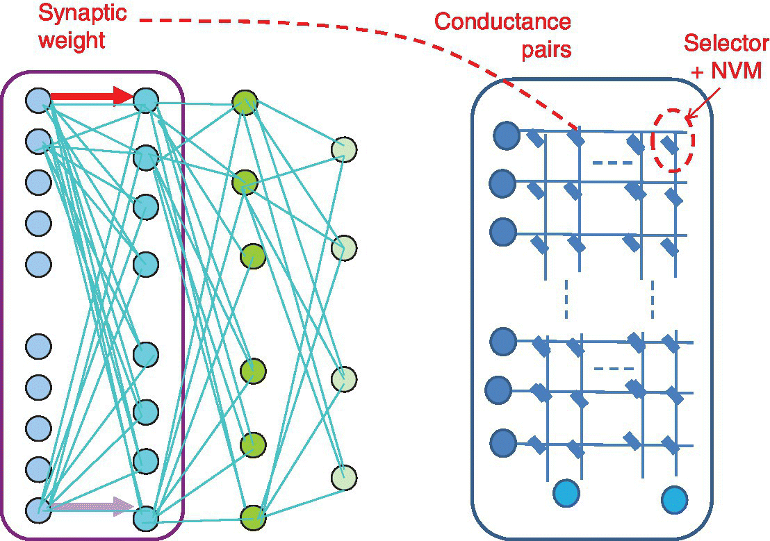
Figure 5.44 An illustration of neuromorphic non‐von Neumann computing.
Based on A. Fumarola et al. (IBM, Pohang University, EPFL‐Lausanne), ICRC, October 2016 [47].
This paper explored the use of NVM and other analog‐type devices for artificial neural networks trained with a back‐propagation algorithm. The advantage of phase change memory synapses over the speed and power of GPU‐based training had been previously shown and this work assessed the impact of undesirable time‐varying conductance change and the trade‐offs in designing peripheral circuitry for artificial neural networks.
The benefit of performing computations at the location of the data is in both power and speed.
Another benefit is in the security of data when it does not need to be stored in the cloud but is processed locally. The computations of training using NVM‐based synapses must be competitive with that using CPUs or GPUs.
Any on‐chip accelerator should be applicable toward networks of different types, such as fully connected deep neural nets or convolutional NN or for networks of different shapes. It was shown that for speed and power of on‐chip machine learning, nonvolatile memory‐based synapses can potentially offer lower power and faster training than GPU‐based training for both large and small networks. A critical factor is the design of area‐efficient read/write circuitry so that many copies of this circuitry are able to operate in parallel.
Using 2 PCM devices per synapse, a three‐layer perceptron with 164 885 synapses was trained with back‐propagation on a subset of the MNIST database of handwritten digits using a modified weight update rule compatible with NVM + selector crossbar arrays. It was shown that this weight update modification does not degrade the high accuracies that a three‐layer network inherently delivers when trained in software. Nonlinearity and asymmetry in the PCM conductance response limited both training and test accuracy. The asymmetry between the gentle conductance increases of PCM partial SET and the abruptness of PCM RESET was lessened by an occasional RESET strategy, which could be both infrequent and inaccurate. Tolerance results showed that all NVM‐type ANN could be expected to be highly resilient to random effects such as variability, yield, and stochasticity, but very sensitive to gradient effects that act to steer all synaptic weights. These observations were extended to assess the impact of undesigned, time‐varying conductance change including drift and leakage of analog CMOS capacitors. A feature of PCM is resistance drift, which is continued relaxation of the material in the amorphous state. The drift is toward an increase in resistance. A potential solution for this issue is a periodic RESET.
PCMO is a nonfilamentary resistance change material in which conductive response was also studied. Resistive switching in PCMO devices is caused by the slow and gradual drift of oxygen ions and vacancies in the polycrystalline PCMO layer. PCMO NVMs show gradual SET and RESET characteristics, but, unlike PCM, there is no need to stop training and perform an occasional RESET operation. RRAM devices based on PCMO can be considered as potentially, providing both a gradual conductance increase and conductance decrease.
5.8.4 Advantages of RRAM over SRAM Crossbar Arrays in Matrix Multiplication
In October of 2015, Sandia National Labs discussed using RRAM crossbar arrays to process large amounts of data for brain‐type computing [48]. Analog computation on a crossbar provides fundamental energy scaling advantages over digital memories. The two key computational kernels that are more efficient on a crossbar include: performing a parallel read or a vector matrix multiply and performing a parallel write where every weight is programmed based on the outer product of the row and column inputs. These two computational kernels comprise the basis of neuromorphic algorithms.
For a parallel analog matrix multiply each column of the crossbar performs a vector dot product for a column. Inputs are represented by a voltage or length of a voltage pulse. Weights are represented by the RRAM conductances. The multiplication is done by summing currents. The minimum energy to read the crossbar is determined by the thermal noise of each RRAM.
For a larger crossbar or a higher voltage due to access devices, the energy will be capacitance limited. Even for a capacitance limited read energy, however, the device will still be more energy efficient than a matrix stored in an SRAM array since SRAMs need to be read out one row or word‐line at a time and the associated circuitry will need to be charged N times for N rows. In an analog RRAM crossbar, everything can be done in parallel so that the circuitry needs only to be charged once. The conclusion was that the energy to perform a parallel read or parallel write on an analog N × N RRAM crossbar array scales as O(N2) while a digital implementation scales as O(N3).
5.9 Neuromorphic Memories Using Polymer and Flexible Memories
Synaptic behavior in flexible IZO transistors on plastic substrates was discussed in November of 2013 by Nanjing University and the Chinese Academy of Science [49]. Flexible IZO transistors were used for synapses in neural computers. Synapses are the connections between neurons and give neurons computational abilities. In this study, indium–zinc oxide (IZO) was used for flexible synaptic EDL transistors made on a plastic substrate using a self‐assembly method at room temperature. The gate dielectric was made of proton conducting phosphorus‐doped nanocrystal SiO2 electrolyte. Excitatory post‐synaptic current, paired pulse facilitation, and long term memory are implemented in the flexible artificial synapses. These IZO flexible electronic synapses have potential for building neuromorphic systems. A schematic diagram of the self‐assembled flexible IZO‐based transistors is shown in Figure 5.45.

Figure 5.45 Schematic diagram of self‐assembled flexible IZO transistors.
Based on J. Zhou et al. (Nanjing University, CAS), IEEE Electron Device Letters, November 2013 [49].
These flexible EDL transistors show an excitatory synaptic current, which is analogous to that found in biological synapses. Pre‐synaptic spike duration time‐dependent excitory post‐synaptic currents are observed in such synaptic transistors because of the slow response of protons in the electrolyte film. Long term plasticity is also represented in the flexible IZO‐based synaptic transistor. Flexible artificial synapses such as these are precursors in building neuromorphic systems. These flexible electronic synapses have potential applications for building neuromorphic circuits.
Organic copolymer RRAM used as a synapse in a neuromorphic system was discussed in December of 2013 by CNR‐IMEM [50]. An organic RRAM/memristor was used to represent a synapse in a neuromorphic system. The analogy with synapses was demonstrated by showing the artificial circuit to mimic part of the nervous system of a low level animal (a pond snail). A stochastic network made of block copolymers, polyaniline, and gold nanoparticles was described. Similarities of the network and the primitive nervous system were observed and various training algorithms were applied; features similar to imprinting/learning were observed.
The working principle of the device was based on the difference in conductivity of polyaniline in the oxidized and reduced states. A thin polyaniline layer was used in the organic RRAM device with a line of solid electrolyte composed of Li+ salt‐doped polyethylene oxide where all redox reactions occur. The variation of the conductivity is accompanied by the migration of Li+ ions between the polyaniline and the polyethylene oxide layers. The device must increase its conductivity with the frequency of its involvement in the formation of signal transfer pathways for learning to occur.
To construct a structure similar to the human brain, a 3D organization of neurons is needed rather than a planar structure. Structuring and supporting random 3D architectures is difficult and the approach used was a bottom‐up self‐organization method using block‐copolymers with phase separation in the formed layers. The main component of the network was a synthesized copolymer with alternating parts of solid electrolyte (polyethylene oxide) and an insulator that acted as a doping agent to polyaniline. The copolymer was mixed with polyaniline and gold nanoparticles, which acted as threshold elements forming Schottky barriers due to the difference in work function between gold and polyaniline. Future work is planned to combine networks of organic devices with living biological objects such as microentities of slime mold.
Polymer RRAM used for neuromorphic applications was discussed in June of 2014 by East China University of Science and Technology, the Chinese Academy of Sciences, and Fudan University [51]. Polymer materials are attractive for implementing RRAM devices due to their low cost, easy processing, mechanical flexibility, and tunable electronic performance and compatibility with CMOS technology. The polymer RRAM is nonvolatile, fast, has low power consumption, a large ON/OFF ratio, high endurance, and long retention. The analog RRAM has the ability to emulate the fundamental synaptic functions of plasticity, which are spike timing‐dependent plasticity (STDP), spike‐rate dependent plasticity (SRDP), and learning behaviors.
Organic memristors in neuromorphic networks used as analogs of synapses were discussed in November of 2015 by the University of Parma [52]. Organic memristive device‐based circuits were explored for biology inspired processing of information. The memristive devices were used in neuromorphic networks and mimicked some of the properties of the human nervous system. The memristive devices were used as electronic analogs of biological synapses.
The synaptic behavior of RRAM made with Ag nanoparticles on flexible substrate was discussed in July of 2016 by Fudan University [53]. The switching behavior of TaN/Al2O3:Ag:AnO//ITO RRAMS made on flexible substrates was considered. A schematic cross‐section of the proposed device is shown in Figure 5.46.

Figure 5.46 Schematic cross‐section of TaN/Al2O3:Ag:AnO/ITO RRAM on flexible substrate.
Based on D.T. Wang et al. (Fudan University), IEEE Electron Device Letters, July 2016 [53].
Intended applications were flexible nonvolatile memory for wearable electronics applications and neuromorphic computers. Embedded Ag nanoparticles give improved device yield and reduce variability in resistance from over 160 to 30%. They also give reduced variability in SET voltage from 35 to 18% and for RESET voltages from 40 to 11% respectively.
Synaptic behavior was shown in this flexible device, which gave it potential for use in neuromorphic circuit applications. Its low power requirements make it closer to emulating biological systems. An effective method was developed to improve flexible RRAM characteristics by coating Ag nanoparticles. The fabricated flexible RRAM showed a high ON/OFF ratio, low resistance fluctuations, high speed, low SET/RESET voltage, low power, and good retention compared to previously reported flexible RRAM devices. Synaptic behavior was shown, which can be used to emulate synapses.
The pulse response of the devices with Ag nanoparticles is plotted in Figure 5.47. Figure 5.47 (a) shows 50 potentiation sweeps of 0.5 V for 150 ms and (b) shows 200 depression sweeps of –0.5 V for 150 ms. After each pulse, the device was measured at 100 mV read pulse and the read current was plotted. It was concluded that embedded Ag nanoparticles in RRAM could be used to mimic the synapse when integrated in a flexible system.


Figure 5.47 RRAM pulse response with Ag nanoparticle: (a) potentiation sweep and (b) depression sweep.
Based on D.T. Wang et al. (Fudan University), IEEE Electron Device Letters, July 2016 [53].
Organic neuromorphic chips for an efficient human–machine interface were discussed in September of 2016 by the University of Minnesota and the Gwangju Institute of S&T [54]. Their results were expected to incorporate organic electronics into large area neuromorphic systems with complex logic circuits and transparent multifunctional interfaces for direct optical and cellular stimulation. Even though these circuits do not compete with inorganic electronics in performance, the ability of the organic neuromorphic technology to mimic functions of biocompatibility were considered promising for large area applications and for direct biointerfacing hybrid systems. An organic synapse concept is proposed where organic‐based neuromorphic devices based on widely available materials can be a route to advance memory circuits and functional neuro‐inspired electronics. The organic FET‐based synaptic devices were constructed on top of a flexible transparent polyelthlene terephthalate substrate with a stack of ITO/PEDOT PMMA. An ultrathin metallic film with a tunneling layer is formed using ambient oxidation and used for the transistor structure for short‐term charge retention. The device had a self‐formed floating gate that was used as a memory.
Organic NVM devices with more than 500 distinct conductance states were discussed in February of 2017 by Stanford University, the University of Groningen, Sandia National Labs, and the University de Sao Paulo [55]. The use of a nonvolatile organic electrochemical device was considered as a low voltage artificial synapse for neuromorphic computing. The electrochemical neuromorphic organic device (ENODe) operates with a fundamentally different mechanism from existing RRAMs. ENODe switches at low voltage and low energy of <10 pJ for 103 µm2 area devices. Over 500 distinct, nonvolatile conductance states are exhibited within a 1 V range. High classification accuracy was achieved when implemented in neural network simulations. The plastic ENODes were made on flexible substrates enabling the integration of neuromorphic functions on stretchable electronics substrates.
References
- 1 Yu, S. (2014) Orientation classification by a winner‐take‐all network with oxide RRAM based synaptic devices (ASU), ISCAS, pp.1058, June 2014.
- 2 Woo, J. et al. (2016) Multilevel conductance switching of a HfO2 RRAM array induced by controlled filament for neuromorphic applications (POSTECH), SNW, June 2016.
- 3 Woo, J. et al. (2016) Improved synaptic behavior under identical pulses using AlOx/HfO2 bilayer RRAM array for neuromorphic systems (Pohang University). IEEE Electron Device Letters, 37 (8), August 2016.
- 4 Woo, J. et al. (2016) Optimized programming scheme enabling linear potentiation in filamentary HfO2 RRAM synapse for neuromorphic systems (Pohang University), IEEE Trans. Electron Devices, 63 (12), December 2016.
- 5 DeSalvo, B. et al. (2015) From memory in our brain to emerging resistive memories in neuromorphic systems (CEA LETI), International Memory Workshop, May 2015.
- 6 Zhang, W. (2015) An electronic synapse device based on solid electrolyte resistive random access memory (Xidian University, NCKU, National Sun Yet‐sen University, Xiamen University, NCTU), IEEE Electron Device Letters, 36 (8), August 2015.
- 7 Clermidy, F. et al. (2014) Advanced technologies for brain‐inspired computing (CEA‐LETI, CEA‐LIST, INRIA), ASP‐DAC, January 2014.
- 8 Jang, J., Park, S., Jeong, Y. and Hwang, H. (2014) ReRAM‐based synaptic device for neuromorphic computing (Pohang University, Gwangju Institute of Science and Technology), ISCAS, pp. 1054, June 2014.
- 9 Jang, J.W. et al. (2015) Optimization of conductance change in Pr1‐xCaxMnO3‐based synaptic devices for neuromorphic systems (Pohang University of Science and Technology, Gwangju Institute of Science and Technology, IBM). IEEE Electron Device Letters, 36 (5), May 2015.
- 10 Moon, K. et al. (2016) Analog synapse device with 5‐b MLC and improved Data Retention for neuromorphic system (Pohang University of Science and Technology, Gwangju Institute of Science and Technology, IMEC‐Leuven). IEEE Electron Device Letters, 37 (8), August 2016.
- 11 Chou, T. et al. (2015) Neuromorphic pattern learning using HBM electronic synapse with excitatory and inhibitory plasticity (National Chiao Tung University), VLSI‐TSA, April 2015.
- 12 Lee, M.‐S. et al. Implementation of short‐term plasticity and long‐term potentiation in a synapse using Si‐based type of charge‐trap memory. IEEE Trans. on Electron Devices, 62 (2), February 2015.
- 13 Sharma, A. et al. (2015) Novel CMOS‐compatible a‐Si based oscillator and threshold switch (Carnegie Mellon University), ESS‐DERC, September 2015.
- 14 Wang, T. et al. (2014) 3D synaptic architecture with ultralow sub‐10 fJ energy per spike for neuromorphic computation (National Chiao Tung University), IEDM, December 2014.
- 15 Gaba, S., Sheridan, P., Du, C. and Lu, W. (2014) 3‐D vertical dual‐layer oxide memristive devices (University of Michigan). IEEE Trans. on Electron Devices, 61 (7), 2581, July 2014.
- 16 Piccolboni, G. et al. Investigation of the potentialities of vertical resistive RAM (VRRAM) for neuromorphic applications (CEA, LETI, Minatec, IM2NP, IMEP‐LAHC), IEDM, December 2015.
- 17 Piccolboni, G. et al. Vertical CBRAM (V‐CBRAM): from experimental data to design perspectives (CEA, LETI, Minatec), IMW, May 2016.
- 18 Li, H. et al. (2016) Four‐layer 3D vertical RRAM integrated with FinFET as a versatile computing unit for brain‐inspired cognitive information processing (Stanford University, NNDL Narlabs), VLSI, June 2016.
- 19 Adam, G.C. et al. (2016) Highly‐uniform multi‐layer ReRAM crossbar circuits (University of California Santa Barbara), ESSDERC, September 2016.
- 20 Gupta, I. et al. (2015) A cell classifier for RRAM process development (University of Southampton, Imperial College, London). IEEE Trans. on Circuits and Systems – II Express Briefs, 62 (7), July 2015.
- 21 Gao, B. et al. (2016) Oxide‐based analog synapse: physical modeling, experimental characterization, and optimization (Tsinghua University, Peking University, Southern University of S&T), IEDM, December 2016.
- 22 Ielmini, D. et al. (2016) Neuromorphic computing with hybrid memristive/CMOS synapses for real‐time learning (Politecnico di Milano, IU NET), ISCAS, May 2016.
- 23 Ambrogio, S. et al. (2016) Neuromorphic learning and recognition with one‐transistor–one‐resistor synapses and bistable metal oxide RRAM (Politecnico di Milano, Micron Technology). IEEE Trans. on Electron Devices, 63 (4), April 2016.
- 24 SAmbrogio, S. et al. (2016) Novel RRAM‐enabled 1T1R synapse capable of low‐power STDP via burst‐mode communication and real‐time unsupervised machine learning (Politecnico di Milano, Micron Technology), VLSI, June 2016.
- 25 Yao, P. et al. (2015) The effect of variation on neuromorphic network based on 1T1R memristor array (Tsinghua University, Tshinghua National Laboratory), NVMTS, October 2015.
- 26 Moon, K. (2016) ReRAM‐based analog synapse and IMT neuron device for neuromorphic system (POSTECH), VLSI‐TSA, April, 2016.
- 27 Mahalanabic, D. et al. (2016) Demonstration of spike timing dependent plasticity in CBRAM devices with silicon neurons (Arizona State University), ISCAS, May 2016.
- 28 Park, J. et al. (2016) TiOx‐based RRAM synapse with 64‐levels of conductance and symmetric conductance change by adopting a hybrid pulse scheme for neuromorphic computing (Pohang University). IEEE Electron Device Letters, 37 (12), December 2016.
- 29 Werner, T. et al. (2016) Experimental demonstration of short and long term synaptic plasticity using OxRAM multi k‐bit arrays for reliable detection in highly noisy input data (CEA, LETI, MINATEC, CEA, LIST, INSERM), IEDM, December 2016.
- 30 Kaneko, Y., Nishitani, Y., Ueda, M. and Tsujimura, A. (2013) Neural network based on a three‐terminal ferroelectric memristor to enable on‐chip pattern recognition (Panasonic), VLSI Technology Symposium, June 2013.
- 31 Nishitani, Y., Kaneko, Y. and Ueda, M. (2014) Artificial synapses using ferroelectric memristors embedded with CMOS circuit for image recognition (Panasonic), Device Research Conference, pp. 297, June 22, 2014.
- 32 Kaneko, Y., Nishitani, Y. and Ueda, M. (2014) Ferroelectric artificial synapses for recognition of a multishaded image (ATRL Panasonic). IEEE Trans. on Electron Devices, 61 (8), August 2014.
- 33 Wang, Z. et al. (2014) Compact modeling of ferroelectric tunnel memristor and its use for neuromorphic simulation (University of Paris‐Sud, Beihang University). Applied Physics Letters, 104, 053505, February 2014.
- 34 Kim, E., Kim, K. and Yoon, S. (2016) Investigation of the ferroelectric switching behavior of P(VDF‐TrFE)‐PMMA blended films for synaptic device applications. Journal of Physics D: Applied Physics, January 2016.
- 35 Suri, M. et al. (2012) Interface engineering of PCM for improved synaptic performance in neuromorphic systems (CEA‐LETI, CEA‐LIST, IEMN), IMW, May 20, 2012.
- 36 Bichler, O., Suri, M., Querlioz, D. et al. (2012) Visual pattern extraction using energy‐efficient “2‐PCM Synapse” neuromorphic architecture (CEA‐LIST, CEA‐LETI, MINATEC). IEEE Trans. on Electron Devices, 59 (8), 2206, August 2012.
- 37 Eryilmaz, S.B. et al. (2013) Experimental demonstration of array‐level learning with phase change synaptic devices (Stanford University, University of Pennsylvania, IBM), IEEE IEDM, December 2013.
- 38 Kim, S. et al. (2015) NVM neuromorphic core with 64 k‐cell (256‐by‐256) phase change memory synaptic array with on‐chip neuron circuits for continuous in‐situ learning (IBM), IEDM, December 2015.
- 39 Hosseini, P. et al. (2015) Accumulation‐based computing using phase‐change memories with FET access devices (University of Oxford, IBM, University of Exeter), IEEE Electron Device Letters, 36 (9), September 2015.
- 40 Burr, G.W. et al. (2016) Recent progress in phase‐change memory technology (IBM, Macronix). IEEE Journal of Emerging and Selected Topics in Circuits and Systems, 6 (2), June 2016.
- 41 Yu, S., Kuzum, D. and Wong, H. (2014) Design considerations of synaptic device for neuromorphic computing (ASU, Stanford, University of Pennsylvania), ISCAS, pp.1062, June 2014.
- 42 Kadetotad, D. et al. (2014) Neurophysics‐inspired parallel architecture with resistive crosspoint array for dictionary learning (Arizona State University), Biomedical Circuits and Systems Conference, October 22, 2014.
- 43 Gao, B. et al. (2014) Origin and suppressing methodology of intrinsic variations in metal‐oxide RRAM based synaptic devices (Peking University), ICSICT, October 28, 2014.
- 44 Kang, J.F. et al. (2015) RRAM based synaptic devices for neuromorphic visual systems (Stanford University), IEEE International Conference on Digital Signal Processing (DSP), July 21, 2015.
- 45 Chen, Z. et al. (2015) Optimized learning scheme for grayscale image recognition in a RRAM based analog neuromorphic system (Peking University, Sandisk), IEDM, December 2015.
- 46 Yu, S. et al. (2016) Binary neural network with 16 Mb RRAM macro chip for classification and online training (Arizona State University, Tsinghua University), IEDM, December 2016.
- 47 Fumarola, A. et al. (2016) Accelerating machine learning with non‐volatile memory: exploring device and circuit tradeoffs (IBM, Pohang University, EPFL‐Lausanne), ICRC, October 2016.
- 48 Agerwal, S. (2015) The energy scaling advantages of RRAM crossbars (Sandia Labs), European Sensory Science Society (E3S), October 2015.
- 49 Zhou, J., Wan, C., Zhu, L. and Wan, Q. (2013) Synaptic behaviors mimicked in flexible oxide‐based transistors on plastic substrates (Nanjing University, CAS). IEEE Electron Device Letters, 34 (11), 1433, November 2013.
- 50 Erokhin, V. (2013) Organic memristive devices: architecture, properties and applications in neuromorphic networks (CNR‐IMEM), ICECS, December 8, 2013.
- 51 Chen, Y. et al. (2014) Polymer memristor for information storage and neuromorphic applications (Chinese Academy of Science, Fudan University, East China University of Science and Technology), Materials Horizons, June 2014.
- 52 Erikhin, V. (2015) Organic memristive devices based circuits for bio‐inspired memorizing and processing of the information (University of Parma), MEMRISYS, November 8, 2015.
- 53 Wang, D.T. et al. (2016) Resistive switching and synaptic behaviors of TaN/Al2O3/ZnO/ITO flexible devices with embedded Ag nanoparticles (Fudan University). IEEE Electron Device Letters, 37 (7), July 2016.
- 54 Kim, C.H., Sung, S. and Yoon, M.H. (2016) Synaptic organic transistors with a vacuum‐deposited charge‐trapping nanosheet (Gwangju Institute of Science and Technology), Science Reports, September 2016.
- 55 van de Burgt, Y. et al. (2017) A non‐volatile organic electrochemical device as a low‐voltage artificial synapse for neuromorphic computing (Eindhoven University of Technology, Stanford, University of Groningen, Sandia National Laboratory, University of Sao Paulo), Nature Materials, February 2017.