
2
Memory Applications for the Intelligent Internet of Things
2.1 Introduction
The Intelligent Internet of Things (IoT) is a term used here for smart networks of processing systems communicating with each other, analyzing the data generated, and responding to the conclusions of this analysis. These networks are expected to improve smart automation in many fields. Examples of such smart networks of systems communicating with each other are: wearable medical devices that take data and transmit it regularly to the network to aid in medical monitoring and evaluation of patients; networks in smart houses that detect motion, fire, smoke, state of door locks; and control cameras or audio devices and turn on/off household equipment under the guidance of a smart network controller. Communicating tags are used everywhere on IoT sensors and they need to be very low cost and work with very low levels of intermittently harvested energy. Energy harvesting is a requirement for the many sensors required in such ubiquitous networks since replacing batteries would be prohibitive. Where batteries are used, ultralow power is required. The many devices used in an IoT network must be very low cost.
Data storage is needed in smart networks. Memories are required to collect the information and process it. Many microcontroller units (MCUs) for IoT have the required memory embedded in the processor. In addition, the processors themselves must have near zero power consumption in standby since most of their time will be spent there. They may need in some cases to power up in the state required without taking time and power to boot‐up. This can be done using nonvolatile nodes in the processors, which can be implemented in some cases using high endurance memory devices such as ferroelectric RAMs (FeRAMs) or magnetic RAMs (MRAMs) on these nodes for power gating. For faster program speed for code and data storage and lower program voltage than Flash memory, resistive RAM (RRAM) could be used. For moderate performance at very low cost, phase change memory (PCM) might be used.
A few of the applications that have been studied for memories for IoT are detailed in this section. These include: ultralow power MCUs with energy harvesting sensors or compact batteries, smart communication tags, networks of wearable medical devices, smart motors, automotive networks, smart meters, and big data search engines.
Annual shipments of MCU with embedded nonvolatile memory were discussed by Renesas in January of 2014 [1]. These are illustrated in Figure 2.1 from 1980 to 2000 along with an indication of the primary embedded nonvolatile memory in each time period: first generation mask ROM, second generation embedded one‐time‐programmable (OTP) memory and third generation embedded Flash. Logic‐based eNVMs are added and a forecast is made to 2020 by extending the data trends. It was estimated by Renesas that MCUs with embedded Flash memories accounted for about 70% of all MCU shipments in 2011.
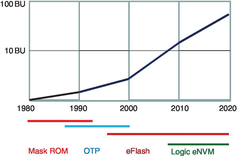
Figure 2.1 Estimate of shipments of MCU chips with embedded nonvolatile memory (BU annually).
Based on T. Kono et al. (Renesas). IEEE Journal of Solid‐State Circuits, January 2014 [1].
2.2 Comparisons of the Various Nonvolatile Embedded Memories Characteristics
2.2.1 Embedded EEPROM, Flash, and Fuse Devices
An early rewriteble embedded nonvolatile memory was the floating gate electrically erasable programmable read only memory (EEPROM) followed soon after by the dual polysilicon Flash memory. Both of these devices were made in the double polysilicon technology still used for standalone devices. Since conventional CMOS logic technology, in which MCUs tend to be made, does not use double polysilicon, the double polysilicon EEPROM and Flash memories added cost to the process when embedded in a processor technology.
Embedded EEPROM and Flash devices that used single polysilicon and were compatible with the conventional CMOS logic technology, were developed in the 1980s. The cost of the technology was lower than for devices made from double polysilicon but the cell size was larger. For very small amounts of embedded memory, a larger cell size was not a significant cost issue. For larger memory capacity or for off‐chip memory, the double polysilicon technology continued to be used.
A comparison between the characteristics of different types of embedded Flash memories can illustrate the trade‐offs between performance and array size. A comparison of various embedded Flash and EEPROMs as a function of array bit count and write cycles was done in October of 2015 by the University of Brescia [2]. Devices considered were: double polysilicon floating gate embedded Flash, single polysilicon EEPROM, transistor‐based antifuse devices, and polysilicon fuse devices. An illustration of the bit‐count versus write cycle characteristics of these embedded Flash memory technologies is shown in Figure 2.2.
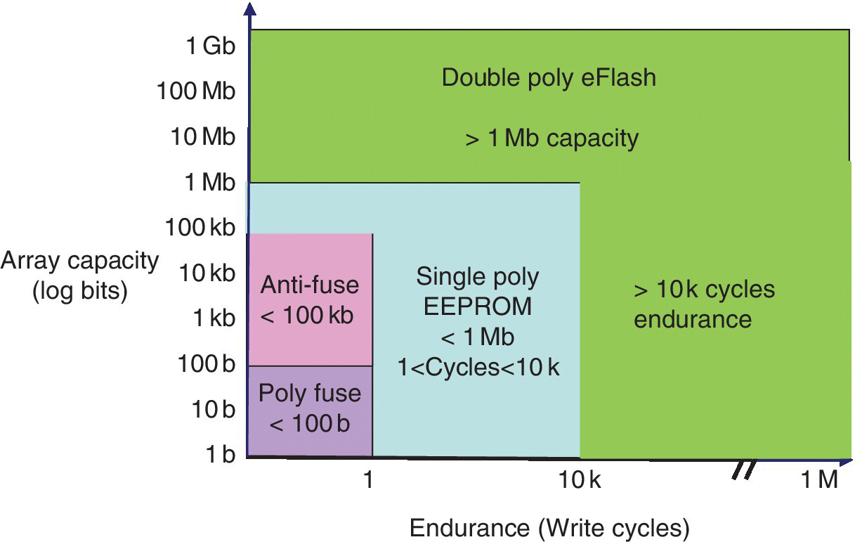
Figure 2.2 Array capacity versus endurance for various types of embedded Flash memory cells.
Based on L. Milani et al. (University of Brescia), IEEE Trans. on Electron Devices, October 2015 [2].
The polyfuse and antifuse solutions for NVM are suitable for one‐time programmable (OTP), small density (<100b) and medium density (<100Kb) applications, but multiple time programmable applications require double poly embedded Flash or single poly EEPROM. The double polysilicon eFlash is suitable for applications of more than 1 M‐bit capacity where the additional cost due to the extra masks and process steps is acceptable. The single poly EEPROM is the best choice for low and medium density applications requiring up to 1 Mb of memory
2.2.2 Embedded Emerging Memory Devices in MCU
Various new memory devices have been investigated to solve the shortcomings of conventional SRAM and Flash storage. These include: magnetic RAM (MRAM), resistive RAM (RRAM), phase change memory (PCM), ferroelectric RAM (FeRAM), and charge trapping Flash memories, such as SONOS, MONOS, and nanoparticle. Many applications discussed here, particularly for IoT, will use the memory embedded in an MCU. The Flash MCU requirements for the various applications differ significantly and affect the type of embedded nonvolatile memory and RAM that can be used in the MCU for that application.
Among the differentiating characteristics of various embedded nonvolatile memories are the endurance to repeated write cycling and the write cycle time. A representation of an analysis done by Qualcomm in June of 2014 of the endurance and write cycle time of various emerging embedded nonvolatile memories is illustrated in Figure 2.3 [3]. This analysis included not only conventional embedded floating gate Flash but also the various emerging memories that are in development and production including: STT‐MRAM, FeRAM, PCM, and RRAM. STT‐MRAM and FeRAM tend to have the longest write cycle endurance, between 1012 and 1015 cycles, and a shorter write cycle time. The 1T1C FeRAM, however, has a destructive read, which means that every read or write cycle affects the endurance. It is, therefore, better suited for applications with limited numbers of read cycles such as datalogging. The 1 T FeRAM does not have a destructive read but is early in its development cycle. PCM and ReRAM have lower endurances at 104 to 106 write cycles with about the same write cycle time as the FeRAM.
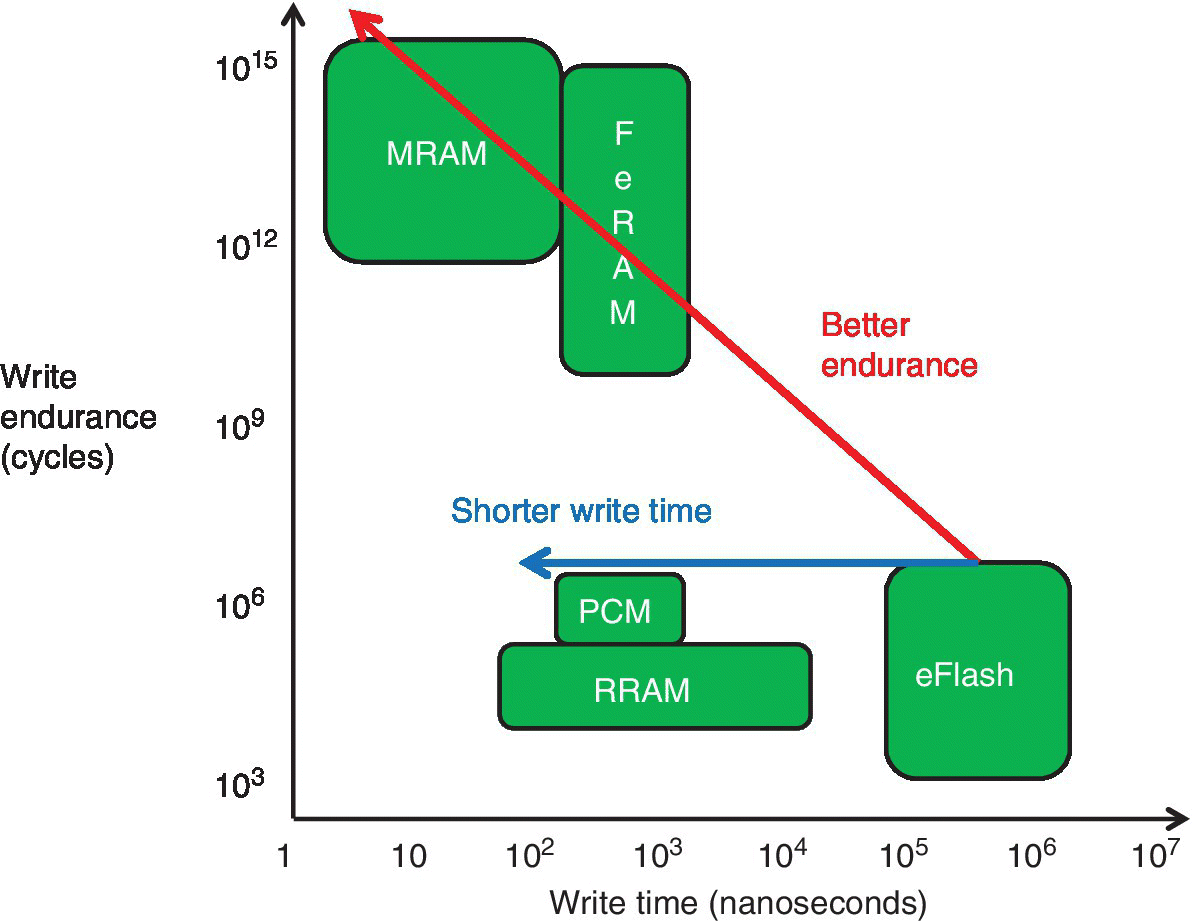
Figure 2.3 Write endurance (cycles) versus write time (ns) for different memory cell types including: SST‐MRAM, FeRAM, PCM, RRAM, and embedded Flash memory.
Based on S.H. Kang (Qualcomm), VLSI Technology Symposium, June 2014 [3].
All of the emerging memories have superior characteristics to the conventional embedded Flash. The STT‐MRAM and the FeRAM have better write endurance and shorter write times than the eFlash. The PCM and RRAM have a shorter write time but about the same endurance. The characteristics determine to a large extent the application for which the particular memory is better suited.
The growth of the Internet enabled devices has created many applications that rely on communication between multiple devices and data storage in these devices. This includes: wearable systems, systems for IoT, and search and storage for big data processing. Nonvolatile embedded memories have become a focus of attention due to the large amount of standby power required for embedded SRAM and the limitations of battery technology. Also of concern is the high program/erase voltages, slow read/write speed, and limited endurance of mainstream Flash memory.
A large number of IoT devices are expected. Gartner has forecast that 6.4 billion connected things (IoT) will be in use worldwide in 2016, up 30% from 2015 [4]. They further forecast that this will reach 20.8 billion by 2020. In January of 2013, Cisco ISBG estimated that 50 billion IoT products would be in existence by 2020 at a value in US$ of 14.4 trillion [5].
2.2.3 Required Properties of Embedded Nonvolatile Memories in Various Applications
While standalone nonvolatile memories have standardized requirements agreed on throughout the industry and defined in industry standards committees among users and vendors, embedded nonvolatile memories have reliability dependent on the specific circuit in which they are embedded and the applications for which the circuit is intended. Typical reliability requirements for embedded nonvolatile memories in general MCU applications were indicated by Samsung in May of 2014 and are shown in Figure 2.4 [6]. The special reliability requirements for smart card and automotive MCU applications were also indicated and are shown in Figure 2.5.
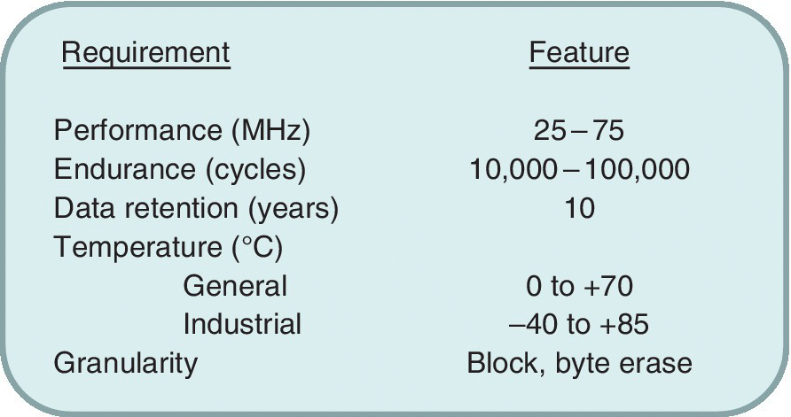
Figure 2.4 Typical reliability requirements for NV memory embedded in MCU.
Based on Y.K. Lee et al. (Samsung), IMW, May 2014 [6].
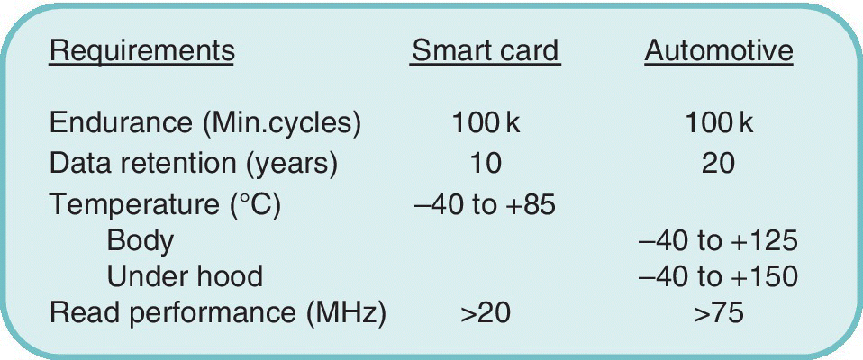
Figure 2.5 Special reliability requirements for nonvolatile embedded memory in MCU for smart card and automotive applications.
Based on Y.K. Lee et al. (Samsung), IMW, May 2014 [6].
Further nonvolatile memory characteristics for various systems intended for IoT applications were discussed by Renesas in April of 2015 [7]. For automotive power train, auto body, and airbag applications, the embedded Flash memory was seen to be adequate for automotive system and performance requirements. As the number of connected systems and the functionality of those systems rose in 2015 for automotive systems, the performance increased for power train, body, and airbag applications. The embedded nonvolatile memory type preferred in Automotive Systems remained the eFlash macro, as shown in Figure 2.6, which indicates the automotive system and performance requirements in 2015.

Figure 2.6 Automotive system and performance requirements in 2015.
Based on T. Yamauchi (Renesas), VLSI‐TSA, April 27, 2015 [7].
These requirements are changing rapidly as the smart connected applications evolve and numbers given here are only indications at a point in time. Automotive electronics remains one of the largest of the Flash MCU sectors. New automotive applications include body and engine processors, infotainment, and driving aids up to completely autonomous cars. Automotive requirements are stringent and include a wide operational temperature range along with high performance and long endurance. This is an application that does not require ultralow power.
Smart card and medical sensors had specification requirements that could be satisfied by embedded Flash memory. For normally off sensor systems it was projected that embedded RRAM or embedded MRAM might also need to be used [7]. Smart cards are another application requiring ultralow power. This includes the rapidly growing bank card application and requires high reliability and secure communications for the card and banking network. Medical devices also required high reliability and secure communications. Smart card and medical device requirements are very different from those of the automotive applications. Power and performance requirements for these systems currently are shown in Figure 2.7. Medical sensors require lower power than smart cards, but do not require the performance at this time, as indicated in the figure.
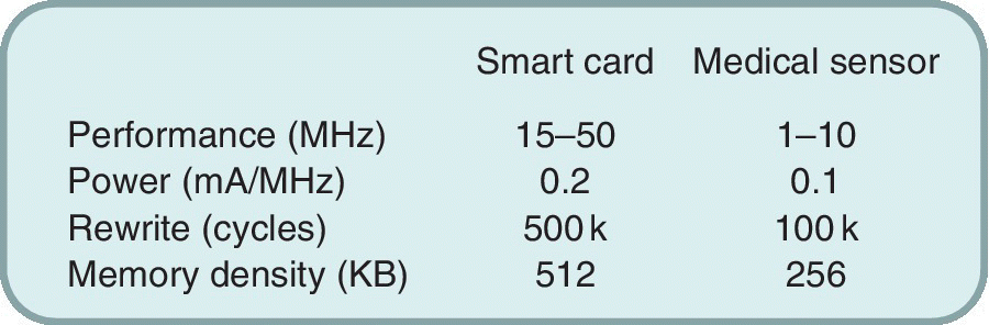
Figure 2.7 Smart card and medical sensor requirements.
Based on T. Yamauchi (Renesas), VLSI‐TSA, April 27, 2015 [7].
Other IoT applications include: networks of digital utility meters, secure home networks, and networks of portable and wearable medical devices. The multiple sensors required in these connected applications require either ultralow power for infrequent changes of batteries or energy harvesting. These criteria are changing constantly and many other applications with differing requirements exist for Flash MCU. The smart electric grid needs network controllers for digital utility meters. Home networks require security and reliable functionality. Secure wireless network chips need smart crypto‐processors while high performance SSD requires integrated storage class memories.
The requirement for the handling of massive data generated by the billions of IoT devices requires large search engines made of nonvolatile memory Ternary CAMs (TCAMs) for high volume data storage in the cloud and at the edge of the Internet perhaps smart computers for processing local data for efficient use. The development of neuromorphic computers with learning capability can perhaps serve this application primarily in vision and hearing analysis. Neuromorphic computers in development are using the analog characteristics of emerging memory chips such as FeRAM, PCM, RRAM, and MRAM.
The predominant types of memory embedded in MCU today are SRAM and Flash NVM with some emerging memories such as FeRAM and RRAM beginning to be used for ultralow power applications. General capabilities of embedded Flash in MCU were discussed by Freescale (now NXP) in May of 2015 and ranged from low end 8‐bit MCU in a 350 nm process, which may have 256 to 512 bytes of Flash, to a high end 32‐bit automotive MCU in a 55 nm process with up to 8.5 MB of Flash memory [8]. Flash memory is used to store boot and application codes, device configuration parameters or personalization information. Requirements are application dependent.
The silicon costs associated with large amounts of embedded Flash in advanced logic processes have to compete with system‐in‐package processes. These systems interconnect discrete memories with an MCU often in stacked chip solution using copper pillar interconnects and through silicon vias (TSV). These packaging costs will come down with time and compete with true embedded Flash. IoT connectivity is causing situations where it is not possible to embed sufficient Flash in the MCU to satisfy the storage requirements for the required amount of data for the application. In this case, integrated MCU and nonvolatile memory system‐in‐package processes might be used. Wafer level integration of high performance memory and processor chips on flexible substrates is also an advancing technology.
Circuits used in IoT applications can be very specialized and require other specifications for the processor and embedded memory. Examples are ultralow power MCU, high speed MCU, and flexible high and low performance devices. In the next section the characteristics of MCU being introduced for some of these specialty applications that occur in the Internet of Things area are discussed.
2.3 Circuits Using Ultralow Power MCU with Embedded Memory for Energy Harvesting
2.3.1 Introduction to Ultralow Power MCU Using Energy Harvesting
Ultralow power MCUs are used today in systems powered by coin batteries or energy harvesters where electrical system energy is not feasible. These MCU serve a variety of IoT applications like wireless home automation, security systems, and wearable medical electronics. In future IoT networks, these applications are more likely to be powered by energy harvesting or coin cell batteries and, as a result, require electronics that consumes very low energy.
The Internet of Things (IoT) uses sensors and MCUs on various devices that are connected through the Internet. With IoT, trillions of sensors are used on devices for collecting information such as temperature, humidity, motion, strain, magnetic field strength, etc. In some cases it is feasible to harvest solar, electromagnetic, or mechanical energy and store it in batteries or capacitors to power these devices.
2.3.2 Ultralow Power MCU with Embedded Flash Memory for Energy Harvesting
Many wireless sensor applications make use of energy harvesting. Ultralow power sensor nodes in wireless sensor networks are being developed for applications such as wearable devices.
A Flash MCU intended for energy harvesting applications was discussed by ST Microelectronics in January of 2014 [9]. This MCU was intended for cost‐sensitive applications and used a low end RISC processor core. Target applications included IoT and smart energy devices. This Flash MCU had 16KBytes to 128KBytes of embedded Flash memory and was expected to bridge the 8‐bit and 16‐bit MCU world. The MCU had crystal‐less USB2.0 and CAN interfaces with a self‐calibrated clock system. It also had a battery charger detection system, controlled power management, and separate power for analog and digital I/Os to support low voltage digital and high voltage analog operation.
2.3.3 Ultralow Power MCU with Embedded FeRAM Memory for Energy Harvesting
It was expected that the energy harvesting applications would require the use of emerging memories with microampere operating and nanoampere standby capabilities. A Texas Instrument’s MCU with an embedded two transistor and two ferroelectric capacitor (2T2C) FeRAM cell was used as an ultralow power processor for this application [10]. This MCU ran up to 25 MIPS. Clock frequencies could be relatively slow ranging, in this case up to 16 MHz. The power supply was specified for battery operation from 1.8 to 3.6 V. The device was optimized for ultralow power mode operation including a 1.7 μA standby current and a 15 nA shutdown current. Active power was typically 126 μA/MHz. The embedded FeRAM memory offered 1015 cycle read and write endurance. The electrical characteristics of the MCU with embedded FeRAM for energy harvesting are summarized in Figure 2.8.

Figure 2.8 Characteristics of an embedded FeRAM MCU for energy harvesting sensor applications.
Based on Texas Instruments Press Release, March 24, 2015 [10].
For computing devices that are transiently powered, such as in energy harvesting systems, the logic state needs to be retained on power down. Such a computing device depends on an intermittent power supply that has bursts of energy that are very short, often less than 100 ms. Purdue University in January of 2014 discussed such transiently powered computers (TPCs) [11]. The primary concern when using conventional embedded Flash memory with higher power processors is that frequent system reboots can result. An SRAM or Flash memory could be used with a battery, but the battery would tend to run down due to the long erase/write time of the Flash memory. A method was followed called Quick Recall, which used ferroelectric memory to enable long running computations in TPCs. This method saved and restored a checkpoint in only 12.6 μs, which is a significantly shorter time than would be required with Flash memory. A Texas Instruments MCU with embedded FeRAM was used. The system showed a significant improvement in program execution time over using an MCU with embedded Flash memory.
Checkpointing performed at previously determined points in the program stored a snapshot of system state in the FeRAM. In case of a fault, the system went back to the most recent check point. To avoid interfering with the normal computations, checkpointing with FeRAM is done only when a drop in the supply voltage occurs. The checkpointing was completed before the power was lost by choosing an appropriate trigger voltage for the FeRAM to begin the checkpointing operation. The program state retained was that of the global variables in use by the program. This study showed that transiently powered computers could do computations even when they receive power for periods as short as 5 ms.
An energy harvesting device can also be made using a low power single ferroelectric transistor (FeFET) memory. An example of an energy harvesting device using an FeFET was given by Panasonic in June of 2014 [12]. The advantage of the FeFET over the 1T1C FeRAM is that the endurance is not affected by a read cycle since the device does not require rewrite after read.
The FeFET energy scavenger used a low cost cantilever‐type 28 μm piezoelectric polyvinylidene fluoride (PVDF) film with a screen printed silver (Ag) ink electrode laminated on to a 0.125 mm polyester substrate. The PVDF cantilever converted energy from mechanical vibration into electric power. A reusable battery‐less impact logging device using a vibration energy scavenger and an FeFET was shown to be functional and suitable for portable use. Figure 2.9 shows the PVDF cantilever in the circuit with the FeFET memory.
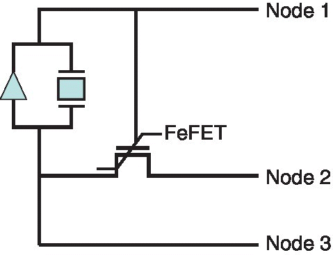
Figure 2.9 Circuit schematic of PVDF piezoelectric vibration energy scavenger cantilever in circuit with FeFET memory.
Based on Y. Kaneko et al. (Panasonic), DRC, June 22, 2014 [12] (permission of IEEE).
The FeFET used a ferroelectric material as a dielectric layer in a MOS FET structure, as shown in Figure 2.10. The FeFET consisted of a stack of ferroelectric Pb(Zr, Ti)O2 (PZT) perovskite oxide film on a 30 nm thick SrRuO2 bottom gate deposited on a sliced stacked trench oxide (STO) substrate by pulsed laser deposition. This combination enabled oriented growth of ZnO on top of the PZT layer with a sharp ZnO/PZT interface.
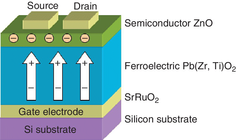
Figure 2.10 Schematic illustration of an FeFET with stacked ZnO/PZT/SrRuO2 structure.
Based on Y. Kaneko et al. (Panasonic), DRC, June 22, 2014 [12] (permission of IEEE).
2.3.4 Ultralow Power MCU with Embedded RRAM Memory for Energy Harvesting
When solar energy is harvested to power an IoT application, a boost converter can be used to increase the solar battery voltage so a nonvolatile memory can be programmed and the sensor data stored. In November of 2015, Chuo University discussed a boost converter for RRAM programming in low power IoT applications [13]. An embedded RRAM was used for the code and data storage since it has faster program speed and smaller program voltage at 3 V than NAND Flash, which uses about 20 V for programming. A RRAM cell was assumed to use 3.0 V SET voltage and 25 μA program current. A representation of the 1T1C structure of the RRAM cell array is shown in Figure 2.11.
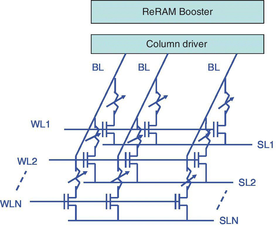
Figure 2.11 Schematic circuit diagram of the 1T1C resistive RAM (RRAM) cell array structure.
Based on T. Ishii et al. (Chuo University), IEEE A‐SSCC, November 2015 [13].
2.3.5 Ultralow Power MCU for Energy Harvesting Power Management
Another circuit using solar energy harvesting was discussed in August of 2015 by Cypress Semiconductor [14]. This family of energy harvesting power management integrated circuits (PMIC) consisted of single chip solar cells as small as 1 cm2 in area. These devices were fully integrated circuits making them a potential for use in smart homes, commercial buildings, and factories. The circuits were able to monitor physical and environmental conditions for these smart buildings.
The solar cells were naturally dependent on placement and available light for energy harvesting applications. Startup power was 1.2 μW and current consumption was as low as 250 mA, which optimized the power available for sensing, processing, and communications depending on the application. A complete, battery‐free energy harvesting system could pair the PMIC with a Bluetooth module for low energy connectivity.
Another energy harvesting device was introduced by TI in 2016 [15]. It was designed to efficiently extract microwatts to milliwatts of power generated from a variety of high output impedance DC sources, such as solar generators or thermal electric generators, without collapsing these sources. Battery management features were used to ensure that the associated rechargeable battery was not overcharged by the extracted power or depleted beyond safe limits by a system load. The cold start voltage was 330 mV. The device allowed continuous energy harvesting from a source as low as 100 mV. Full operating quiescent current was typically 488 nA and the maximum charge current was 100 mA.
2.4 Ultralow Power Battery Operated Flash MCU
2.4.1 Introduction to Ultralow Power Battery Operated Flash MCU
Ultralow power MCUs serve a variety of IoT applications like energy metering, home automation, security systems, industrial control, and portable medical electronics, as indicated in Figure 2.12. These applications are likely to be either powered by energy harvesting or by low current batteries and require very low energy operation along with zero power standby and rapid wakeup from standby.

Figure 2.12 Ultra‐low power IoT battery operated applications used with emerging memory technologies.
Some emerging memory devices, such as RRAM and FeRAM, switch faster than Flash memory, operate at lower voltages, and have a lower operating current. Like Flash memory, they are nonvolatile. MCU with these emerging memories embedded in the processor chip could provide extended battery operating life for portable devices if they are also capable of being manufactured in conventional CMOS processes at low cost.
Ultralow power battery operated Flash MCU require low current consumption to prolong battery life. This low current can be obtained by various current detection and power management control circuits. Separating power for analog and digital circuits can help. Using lower current EEPROMs can also reduce current consumption. Operational modes such as fast wake‐up from standby and longer times in low power states combined with fast switching can also reduce power. Various of these power lowering options that have been used are shown in Figure 2.13. These include: current detection circuits, power management control circuits, separate power for analog and digital circuits, low current EEPROM macros, fast wake‐up from standby and longer times in low power states with fast switching.
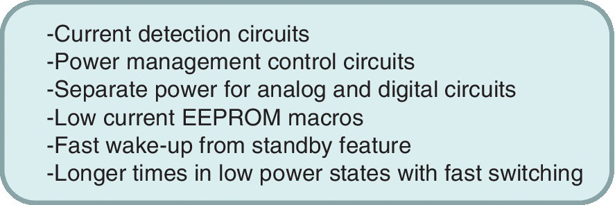
Figure 2.13 Power lowering techniques for ultralow power battery operated Flash MCU systems.
2.4.2 Ultralow Power Battery Operated Flash MCU with Embedded Flash Memory
An MCU with embedded Flash memory, targeted at cost‐sensitive battery powered applications, was announced in January of 2014 by ST Microelectronics [16]. This MCU used 16 KB to 128 KB of embedded Flash memory and a low end RISC processor core. Target applications included IoT and smart energy devices. This series was expected to bridge the 8‐bit and 16‐bit world. The MCU had crystal‐less USB 2.0 and CAN communication interfaces with a self‐calibrated clock system. To help control power consumption, it had battery charger detection and system controlled power management. Separate power for analog and digital I/Os helped to support low voltage digital and high voltage analog operation.
In order to target applications operating on smaller batteries such as wearable devices and industrial sensor networks, lower power consumption was required. In February of 2014, STMicroelectronics announced an ultralow power Flash MCU featuring a 32 MHz RISC processor core, a 100 k sps ADC consuming 40 μA, and crystal‐less USB FS2.0 [17]. Up to 64 KB of Flash memory could be integrated along with 2 KB of embedded EEPROM in the CMOS logic technology. Target applications included fitting smaller coin batteries on portable medical equipment such as fitness trackers and glucose meters. The analog‐to‐digital converter (ADC) consumed 40 μA at 100 k sps and up to 200 μA at 1.14 M sps, so a coin battery could operate a fitness tracker for two years. The CMOS technology had low variation over the –25 to 125 °C temperature range.
An energy efficient MCU with RISC core and embedded Flash memory intended for use in ultralow power IoT applications was introduced by Cypress in November of 2015 [18]. The device was optimized for advanced wearables along with a range of ultralow power battery‐powered products. The MCUs offered up to 560 KB of Flash memory and 64 KB of SRAM. The devices had fast wake‐up time from standby, which minimized power consumption by being able to remain in low power states for longer times before switching briefly to active mode. Active current was 40 μA. The device offered the ability to move data between peripherals and RAM without CPU intervention. Communication interfaces offered advanced encryption standard (AES) hardware encryption. AES is a symmetric block cipher used to protect classified information and to encrypt sensitive data. The communication interfaces included: multifunction serial interfaces, USB, a smart card interface, and I2C for digital audio. Some analog peripherals were included.
2.4.3 Ultralow Power Battery Operated MCU with Embedded RRAM
Ultralow power MCUs that are operated on battery optimize the current available by storing data at a low current level during the write operation so the optimum data storage is obtained. An RRAM discussed by Panasonic in July of 2013 was embedded in an 8‐bit MCU and was intended to replace Flash memory [19]. It had stable low current operation as a result of the electric current being kept constant during the RRAM forming process so that the resulting filaments were uniform. A metal oxide RAM (OxRAM) technology was used for the RRAM. This RRAM used Ta2O5 to control oxide density and defects during the deposition of a tantalum layer. The intended battery‐backed applications require low power operation and include devices such as sensors, security systems, and portable healthcare devices. Electrical and reliability characteristics of 8‐bit MCU with embedded RRAM intended for use in battery powered circuits are shown in Figure 2.14.

Figure 2.14 Electrical and reliability characteristics of 8‐bit MCU with embedded RRAM for use in battery powered circuits. An oxide RAM (OxRAM) technology was used for the RRAM.
Based on Panasonic Press Release, July 30, 2013 [19].
The MCU with the embedded RRAM operated at voltages as low as 0.9 V, which permitted low power consumption. Standby current was 60 nA with a 3 V power supply and an operating current of 200 nA during real time clock operation. Compared to a comparable MCU with embedded Flash (eFlash), the power consumption was about half. In a comparable eFlash MCU, the write voltage was given as 2.7 V and the write speed as 30 μs/byte, while in the MCU with eRRAM, the write voltage was 1.8 V and the write speed was 3 μs/byte.
With the embedded RRAM, the device is turned on for a much shorter time and at lower voltage so less current is consumed. The ‘ewrite cycle endurance for the eRRAM was 100 000 cycles, which is comparable to the eFlash. The RRAM still needed to be installed in the back‐end process, after which it was expected to be usable at various process nodes. The initial production was in Panasonic's 180 nm process. In February of 2017 Panasonic and UMC in Taiwan began joint development of a 40 nm RRAM platform [20].
2.4.4 Ultralow Power Battery Operated MCU with Embedded FeRAM
An embedded FeRAM in a low power MCU was discussed by Texas Instruments in June of 2013 [21]. Standby current consumption was reduced to 350 nA by using critical blocks and other architectural tailoring. Fast wake‐up within 6.5 μs from standby mode or sleep mode was achieved using analog precharge current sources. For the lowest system energy, power management was divided into blocks.
A power management block diagram of the MCU is shown in Figure 2.15. This block diagram illustrates the details of the dedicated power subsystem. The system is partitioned into different power domains in order to power‐off circuitry that is currently unused. A low dropout (LDO) linear regulator is used as a low cost, accurate power supply. The real time clock (RTC) domain is separated so only 350 nA of current is consumed while the RTC is running. The memory FeRAM LDO is also separated. The core domains are power gated. The precharge current sources directly source the power gated domains from the 3 V VCC supply for fast startup of the power gated domains.
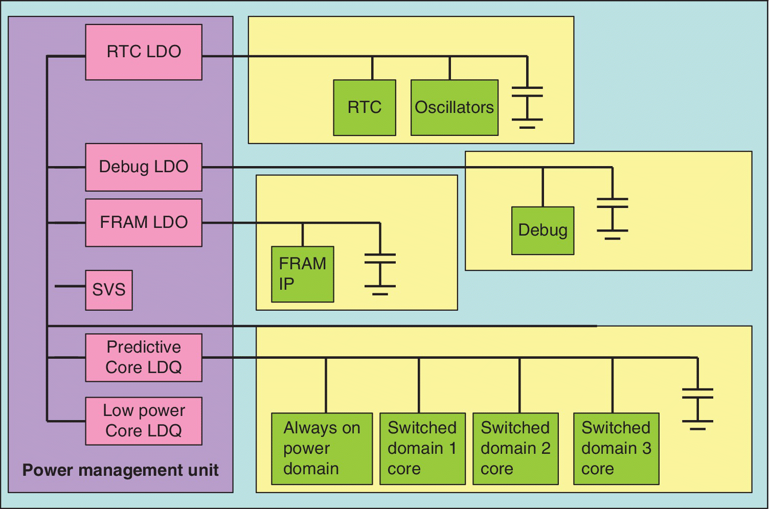
Figure 2.15 Power management block diagram of the low power FeRAM MCU.
Based on A. Baumann et al. (Texas Instruments), VLSI Circuits Symposium, June 12, 2013 [21].
The major blocks consist of the 16‐bit MCU core and digital logic with dedicated power domains for debug and the real time clock (RTC), power management module (PMM), and analog and memories including FeRAM, RAM, and ROM. Features and target applications of the 16‐bit MCU with embedded FeRAM intended for use in battery powered circuits are shown in Figure 2.16.
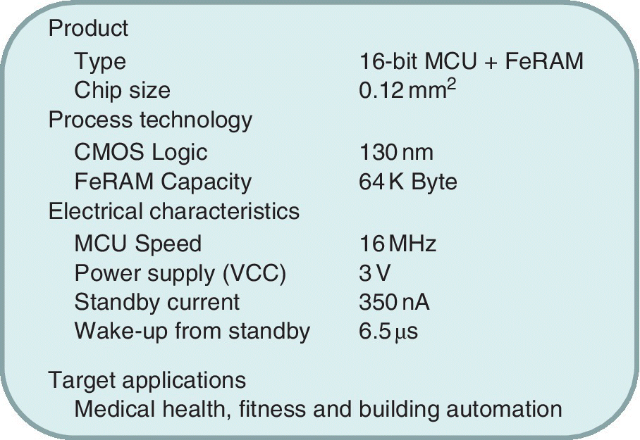
Figure 2.16 Features and target applications of 16‐bit MCU with embedded FeRAM intended for use in battery powered circuits.
Based on A. Baumann et al. (Texas Instruments), VLSI Circuits Symposium, June 12, 2013 [21])
The 130 nm CMOS technology used 5‐layer copper (Cu) metal interconnects. Chip size was 0.12 mm2. The MCU ran at 16 MHz and the FeRAM capacity was 64 KB. A block diagram of the MCU with eFeRAM is shown in Figure 2.17. Blocks shown are: the clock, nonvolatile FeRAM, RAM, and 16b RISC processor.

Figure 2.17 Block diagram of the MCU with eFeRAM.
Based on A. Baumann et al. (Texas Instruments), VLSI Circuits Symposium, June 12, 2013 [21].
Many IoT sensing applications require extended battery life for sensing and measurement applications. In March of 2016, TI announced an MCU with embedded FeRAM that offered a configurable low leakage transimpedance amplifier with 20 times lower leakage than previous solutions and therefore potentially offered an extended battery life [22]. The MCU included a configurable analog, which reduced printed circuit board (PCB) space. The analog integration permitted connecting to a wide range of sensors. It integrated a ferroelectric RAM nonvolatile memory. The fast read and write of the FeRAM permitted configuring the amount of memory allocated for application code or data by eliminating the boundaries between Flash and RAM. The FeRAM MCU offered a higher performance than the previous generation MCU, which used Flash. Applications targeted included: medical health and fitness and building automation. TI proposed adding an energy harvesting IC to extend the battery life even further.
2.5 Nonvolatile MCUs Using Emerging Memory for Nonvolatile Logic
For MCUs in battery powered or energy harvesting applications, it is essential that standby power be ultralow. This can be accomplished in the logic by power gating, which is turning off the power in a block of circuits. If a nonvolatile memory cell is associated with a logic node then the logic state of that node is stored in the event of power‐down and can be restored on startup. This latter technique essentially eliminates standby power. In this case, the MCU does not need to be supplied with power during standby and comes up in the previously stored state when the power is restored.
2.5.1 Nonvolatile Logic Arrays Using FeRAM
The state of a nonvolatile data Flip‐Flop (nvDFF) can be stored in an embedded FeRAM capacitor. In February of 2013, MIT and TI discussed the design of an nvDFF with embedded ferroelectric capacitors that sense data [23]. The nvDFF was integrated into the ASIC design flow with a power management unit and a simple interface to the brown‐out detection circuitry. This design managed power by operating normally “off”. The process technology included embedded ferroelectric (FE) capacitors that store data. Prior to sensing, the FE capacitors are programmed to opposite data states. Identical charging currents integrate the difference in remnant charge between the two FE capacitors, as shown in the circuit schematic in Figure 2.18. The first node to cross the diode voltage drop plus a PMOS threshold pulls the internal node of the sense latch high.
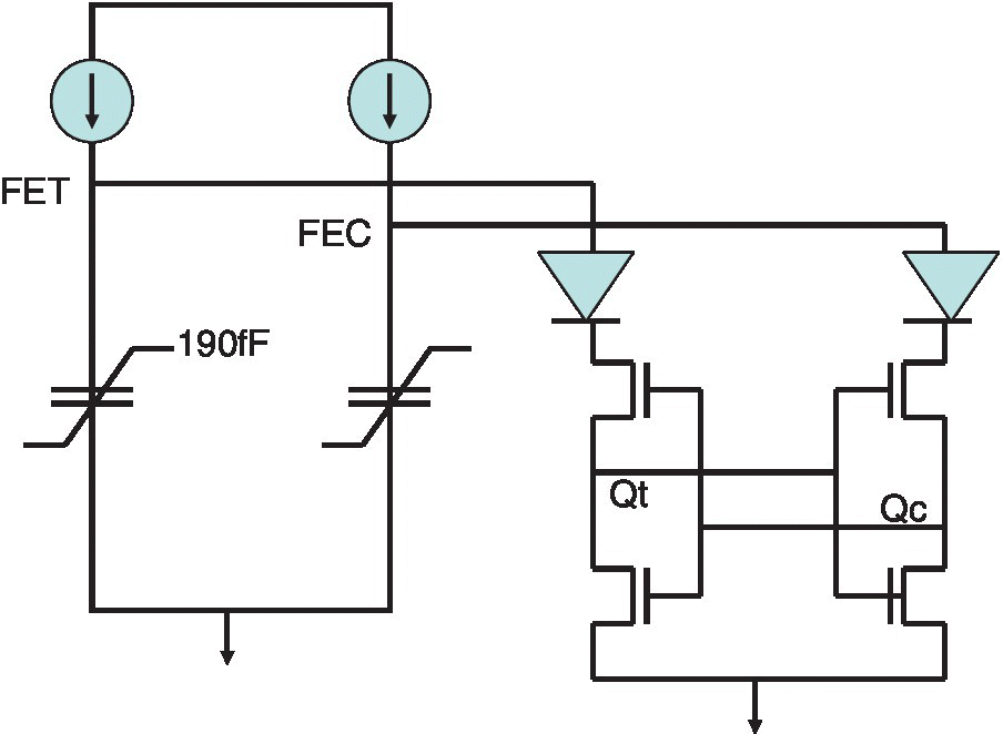
Figure 2.18 Illustration of ferroelectric (FE) capacitors connected to a nonvolatile data flip‐flop (nvDFF).
Based on M. Qazi et al. (MIT, TI), ISSCC, February 2013 [23].
The FIR filter was designed with 96 nvDFFs and about 500 gates. For the target application, which was an MCU, about 5000 nvDFFs were retained. The nvDFF has a split supply rail so sensing current ramps can be perturbed. With zero skew, all nvDFFs in the five measured chips, a total of about 21 000 nvDFFs, operated without failure and the distribution of skew indicated a below 1 ppm failure for an unskewed nvDFF. The additional energy cost from nodes glitching in the FIR filter, cycle overhead, and programmable memory unit (PMU) energy is about 1.780 pJ out of 3.439 pJ.
Commercial ultralow power (ULP) MCUs need to balance different requirements by providing high performance and very low standby power along with fast wake‐up time for various real time applications. In November of 2013, TI and TSMC discussed a full high voltage threshold (HVT) 8 MHz 75 μA/MHz nonvolatile logic (NVL)‐based MCU with zero standby power and fast 384 ns wake‐up time [24]. In this processor, nonvolatile miniarrays are distributed though the logic domain of the MCU, which take a snapshot of the state of all sequential elements before the MCU goes into a power‐gated standby mode. Upon wake‐up, no boot‐up is required.
These miniarrays use ferroelectric capacitors for fast low power nonvolatile state retention. The ferroelectric capacitors are programmable capacitors that retain their programmed state without a power source. The read plus write endurance of the FeRAM is >1015.
A high bandwidth parallel connection between the flip‐flops and miniarrays helped achieve a fast MCU wake‐up. Nonvolatile logic (NVL) had no impact on MCU active mode performance and power. It added only 3.6% to the chip area. Since the NVL eliminates leakage in standby mode, it permits use of high performance leaky processes in MCU design.
The system architecture of the MCU is shown for a second generation full standard voltage threshold (SVT) 32 MHz nonvolatile logic MCU in the block diagram in Figure 2.19. The SVT SoC has four times higher active mode performance or 30% lower active energy than the HVT SoC, but can still achieve zero leakage using the nonvolatile logic. This created a zero leakage fast wake‐up standby mode and also provided benefits in active power and performance. In particular, it is expected to be useful for energy harvesting applications.
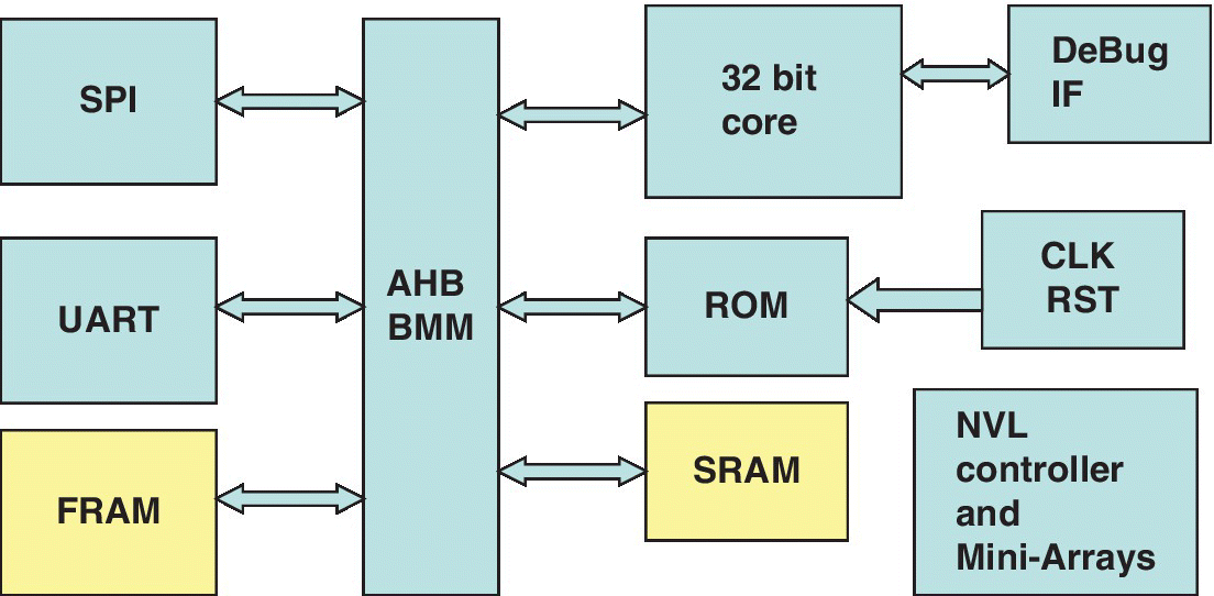
Figure 2.19 System architecture of the MCU showing 32b core and nonvolatile logic (NVL) controller.
Based on S. Khanna et al. (TI, TSMC), A‐SSCC, November 11, 2013 [24].
This 130 nm nonvolatile logic (NVL) based 32b MCU SoC backs up its working state, which includes all flip‐flops, upon receiving a power interrupt. TI reported in January of 2014 that this MCU has zero leakage in sleep mode and requires less than 400 ns to restore the system state on power‐up [25]. A low power technology is used with a 1.5 V power supply. Nonvolatile ferroelectric capacitor‐based miniarrays back up the machine state and permit the chip to wake up instantly after a power cycle. Without the NVL, a chip would either need to keep all flip‐flops powered, which would result in high standby power, or the system would need to spend energy and time rebooting after each power‐up.
NVL permits systems to use leakier processes to achieve higher performance and lower dynamic power while retaining zero leakage in sleep mode. In this case, the addition of the NVL only adds 3.6% to the SoC area. Process cost adders are minimized since only two additional masks are required for the ferroelectric NVL implementation. A functional diagram of the NVL SoC is shown in Figure 2.20.

Figure 2.20 Functional diagram of NVL 32‐bit SoC with FeRAM program and data memory.
Based on S. Khanna et al. (Texas Instruments), IEEE JSSC, January 2014 [25].
The voltage regulation, supply detection and PM state machines are off‐chip. The MCU SoC discussed has zero sleep mode leakage with a 400 ns wake‐up time. The chip has 100% digital state retention. System wake‐up time is reduced from 100 s of microseconds to a few microseconds since no boot‐up is required after a power cycle. Before entering the sleep mode, data from all flip‐flops and latches in the system are transferred to the ferroelectric capacitor‐based NVL arrays.
The NVL can be used in any digital system with two system requirements: the system must be edge triggered synchronous and the clocks for all flip‐flops must be stopped in the inactive state while going into the sleep mode. The SoC has conventional FeRAM memory. The NV elements added to the SoC are tested and the reliability ascertained. NVL bit‐cell read signal margins are measured and there is a test and debug capability.
2.5.2 Nonvolatile Logic Arrays Using MTJ MRAM
Another processor using power gating and a nonvolatile array was described in November of 2013 by Tohoku University and NEC [26]. This power‐gated MPU uses a nonvolatile flip‐flop (nvFF) with a magnetic tunnel junction (MTJ) MRAM type of memory. The nvFF was used to store the MPU’s internal state. The power‐gating operation for this MPU had a 3 μs entry/exit delay penalty during power on and power off. This was one order of magnitude faster than a conventional MPU in deep power‐down mode. An nvFF circuit was developed to obtain this small entry/exit delay with stable fast store and recall. The power‐gated mode was easy to control. This processor core was based on a 32‐bit pipeline architecture.
In the power‐gated MPU, all necessary processor internal states are stored in NV memory. This includes executing programs in the instruction memory and some temporary calculation results in the register file. This means the MPU can immediately return from the suspended state and restart program execution. This move into and from the power‐off mode does not require obtaining or storing data from external memories, which makes the entry/exit delay short. A nonvolatile latch circuit diagram using MTJ MRAM elements in CMOS technology is shown in Figure 2.21.
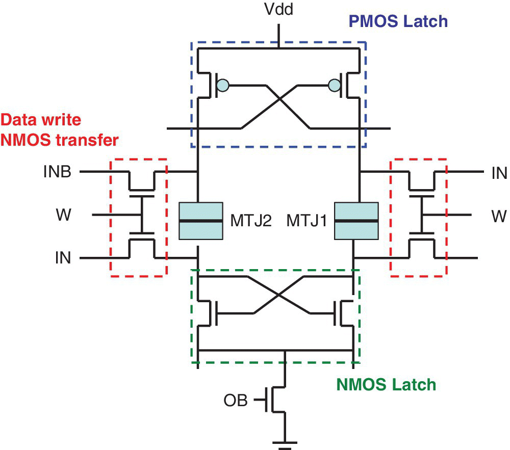
Figure 2.21 Basic NV latch circuit diagram using magnetic tunnel junction (MTJ) nonvolatile memory elements in CMOS technology.
Based on H. Koike et al. (Tohoku University, NEC), A‐SSCC, November 11, 2013 [26]. (Permission of IEEE).
A detailed SPICE simulation analysis of a CMOS/MTJ hybrid circuit was executed and the design and fabrication of a prototype MPU chip was done. Results showed that power gating had a 3 μs penalty for entry/exit delay. This was an order of magnitude faster than for a conventional MPU deep power‐down.
Processors with MTJ‐MRAM nonvolatile arrays can also be used for intermittent operations.
A fully nonvolatile MCU with an embedded emerging NV‐RAM memory was discussed by NEC and Tohoku University in February of 2014 [27]. This 90 nm CMOS 16‐bit MCU used a three transistor SpinRAM memory consisting of two transistors and one MTJ MRAM (2 T + 1MTJ) and was intended for use in applications such as battery‐powered sensor nodes. The MCU operated at 20 MHz with 145 μW operation with a 1 V power supply in the active state and 4.5 μW intermittent operation with a 120 ns wake‐up time and 0.1% active ratio without needing to forward reboot code from memory. Power consumption was sufficiently low that battery powered sensor nodes were effectively free of maintenance. A block diagram of the MCU with embedded SpinRAM memory is shown in Figure 2.22.

Figure 2.22 Block diagram of nonvolatile 65 KB RAM/ROM unified (2T+1MTJ) SpinRAM MCU.
Based on N. Sakimura et al. (NEC, Tohoku University), IEEE ISSCC, February 2014 [27].
The MCU had a 16b RISC CPU core, a 64 KB RAM/ROM unified SpinRAM macro and other logic circuits including timers, a 32‐bit multiplier, a power management module (PMM), universal serial interfaces (USCI), and a direct memory access (DMA) module. It had some redundant words and columns to replace defective cells and an error correction code (ECC) circuit for write failures.
To eliminate backup and restore overhead through the memory bus, 4096 nonvolatile magnetic flip‐flops (MFF) were used to capture the context of the CPU. Two instructions permitted software to flexibly back up and restore data to the MFFs. V cc was 1.8 V to 3.3 V with a 1 V internal power supply provided by a DC/DC converter. The MCU supported three low power modes: standby mode, power‐gating mode and sleep mode. In standby mode, all cores remained on and the main clock was gated, resulting in a 117 μW leakage current. In power‐gating mode, 1.6 μW was consumed with all cores turned off. In sleep mode the DC/DC converter was turned off and static power was zero.
A similar digital system where there is no distinction between ON and OFF and where the computational state is stored in NV Logic elements was discussed in January of 2014 by Cypress, TI, and MIT [28]. This system was intended to operate from harvested energy without requiring reboot. A nonvolatile D‐Flip‐Flop (nvDFF) was designed in 130 nm CMOS technology. The nvDFF was integrated into an ASIC design flow.
A test case nonvolatile FIR filter is discussed with a power management unit that automatically saved and restored the state of a one‐bit indicator of energy availability. Correct operation was verified over power cycle intervals from 4.8 μs to 1 day. The round trip save–restore energy is 3.4 pJ per nvDFF. Measurements were made to validate the capability to make a 10 parts per minute (ppm) failure rate for embedded system applications.
An illustration of the designed operation of nonvolatile processing is shown in the graph in Figure 2.23, which shows VDD plotted against time. The system performs useful computations in between unpredictable interruptions in the availability of harvested energy. During an interruption the data are retained.
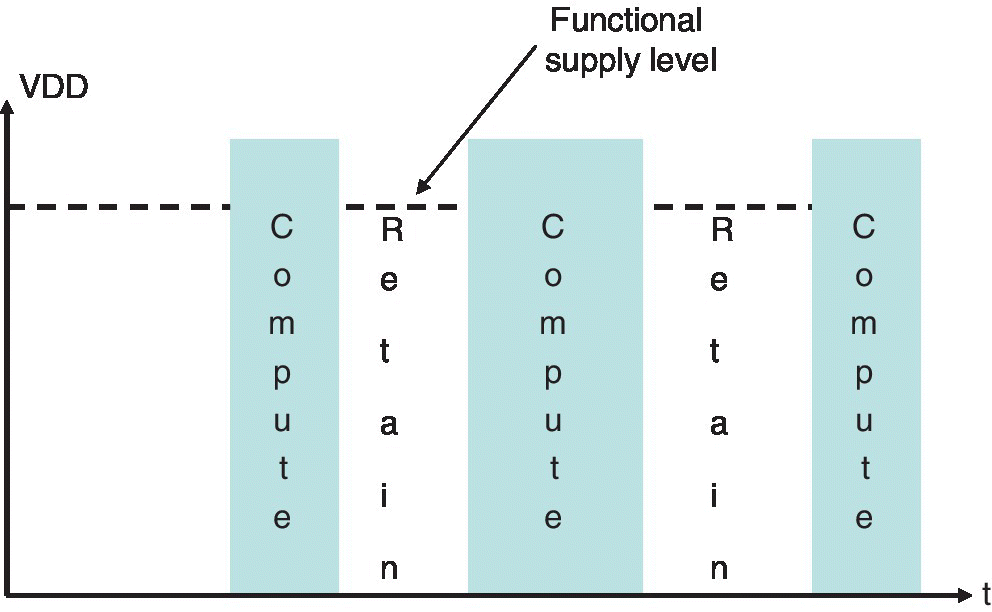
Figure 2.23 VDD versus time of computations in energy harvesting type system with NVDFF showing computations interspersed with times of retained data.
Based on M. Qazi et al. (Cypress, MIT, TI), IEEE Journal of Solid‐State Circuits, January 2014 [28].
2.5.3 Processors with RRAM for Nonvolatile Logic Arrays
The power of many SoCs tends to be dominated by the leakage power of the embedded memories and the status registers. Leakage current and active power can be reduced by power supply scaling to the near threshold range or even into the subthreshold range. Low power memories can also help reduce the leakage. RRAMs are nonvolatile and therefore have low standby power dissipation and can be operated at low voltages. In November of 2014, EPFL, the Swiss Federal Institute of Technology, discussed energy and reliability trade‐offs in a low voltage RRAM‐based nonvolatile flip‐flop (nvFF) design [29]. In this study, RRAM nvFF are optimized for operation in the low voltage and subthreshold ranges. A 180 nm CMOS process was used with a compatible voltage of 2 V and a low current compliance of 10 μA.
Three low voltage nvFF circuits were evaluated for power dissipation and reliability. Topologies are used that have two complementary programmed RRAM devices. Monte Carlo simulations are used to determine parametric variations and confirm data restore operations from the RRAM devices in subthreshold ranges as low as 400 mV. Minimal energy is found for a near voltage threshold (V t) read operation with a total read plus write energy of 735 fJ. A block diagram of a nonvolatile flip‐flop is shown in Figure 2.24. This is a conventional master–slave flip‐flop with write and read registers indicated.

Figure 2.24 Conventional master–slave nonvolatile flip‐flop.
Based on I. Kazi et al. (EPFL), IEEE Trans. on Circuits and Systems, November 2014 [29].
RRAMS can be used in field programmable gate arrays (FPGA) as well as nvFF. In December of 2014, CEA and LETI Minatec discussed RRAMS for both FPGA and for nvFF [30]. In FPGAs, replacing the SRAM with RRAM saves area since the cell size of the RRAM is smaller than that of the SRAM and the nonvolatility suppresses standby power consumption. The leakage current through the RRAM during operation depends on the high resistance state (HRS) value. For this reason, a specific type of RRAM, a conductive bridge RAM (CBRAM) with a dual layer electrolyte stack and resistance ratio (high resistance state divided by low resistance state) greater than 10, was suggested to minimize operating leakage current. The resistance ratio is also called the ON/OFF current ratio. The CBRAM was made of a dual layer of solid electrolyte, HfO2 and GeS2, embedded between an Ag electrode and a W plug.
The use of RRAM in fixed logic circuits such as nvFFs permits zero standby leakage and fast power ON/OFF operation. The requirements for an RRAM in an nvFF are: endurance, low operating voltage, and fast ON/OFF operation. An HfO2/Ti metal oxide RRAM cell, an OxRAM, with less than 10 ns switching time at 1 V and endurance up to 108 cycles was also suggested for this application. This OxRAM’s active layer was HfO2 between TiN and Ti/TiN electrodes. A schematic cross‐section is shown in Figure 2.25. Figure 2.25(a) shows the OxRAM stack and Figure 2.25(b) shows the CBRAM stack with GeS2 and with the HfO2/GeS2 electrolyte with an Ag top electrode and a W bottom electrode. Devices with a large memory window such as the HfO2/GeS2 CBRAM enable high density, low leakage cells for FPGA. Cells with low voltage, time switching, and high endurance such as the HfO2/Ti OxRAM permit a fast switching fixed logic design.
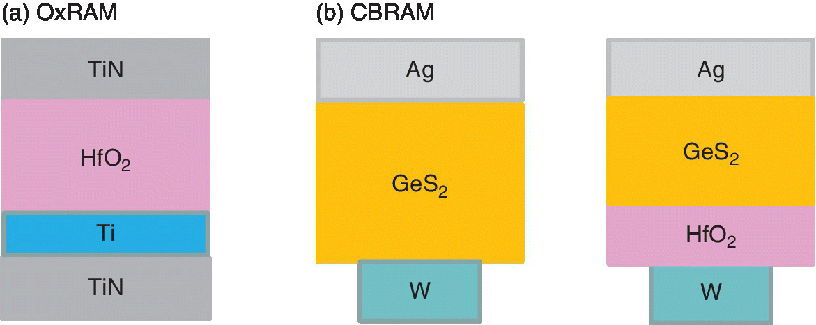
Figure 2.25 Schematic of (a) OxRAM RRAM stack and (b) CBRAM with HfO2/GeS2 electrolyte.
Based on E. Vianello et al. (CEA LETI), IEDM, December 2014 [30].
Nonvolatile SRAMs (nvSRAM) are conventionally constructed using two nonvolatile memory devices and a 6 T SRAM. In June of 2015, several Taiwanese labs and universities discussed an RRAM‐based 7T1R nonvolatile SRAM [31]. The nvSRAM had a two times reduction in stored energy and 94 times reduction in restore energy for frequent‐off and instant‐on applications. The store energy is reduced by using only a single RRAM device rather than the two normally used. Also the DC short current is suppressed during the restore operation by using a pulsed overwrite method. A circuit schematic of the 7T1R nvSRAM cell is shown in Figure 2.26.
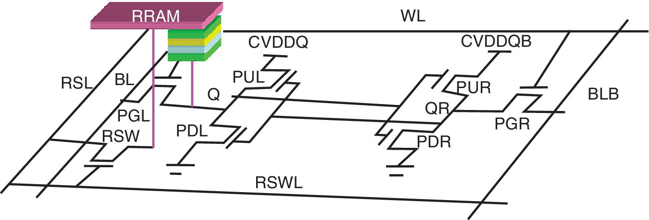
Figure 2.26 3D circuit schematic illustration of 7T1R nvSRAM.
Based on A. Lee (NTHU, NDL, NCHU, EOL ITRI), Symposium on VLSI Technology, June 2015 [31].
A high restore yield was attained by using a differentially supplied initialization method. This initialization and overwrite 7T1R nvSRAM improved breakeven time by 6 times compared to previous nvSRAMS. A 16 K‐bit 7T1R nvSRAM was made using an HfOx RRAM in a 90 nm CMOS process. In SRAM mode the read operation was the same as for the 6 T SRAM. The separation of CVDD lines permitted applying different voltages to VDDQ and VDDQB to improve the write margin.
In February of 2016, Tsinghua University, NTHU, and the University of California, Los Angeles, discussed a 65 nm RRAM enabled nonvolatile processor that had a 6 times reduction in restore time and a 4 times higher clock frequency when using Adaptive Data Retention and Self‐Write termination [32]. The processor used an adaptive nvFlipFlop with RRAM, a code storage RRAM macro, and an adaptive nvSRAM using RRAM. The system architecture of the RRAM enabled nvProcessor is shown in Figure 2.27.
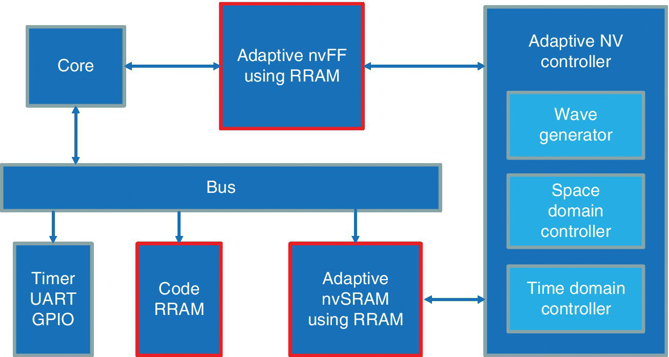
Figure 2.27 System architecture of the RRAM enabled NV‐processor.
Based on Y. Liu et al. (Tsinghua University, National Tsing Hua University, University of California, Los Angeles), ISSCC, February 2016 [32].
A 65 nm fully logic compatible RRAM based nonvolatile processor (NVP) achieved time and space adaptive data retention. A one macro nvSRAM with self‐write termination (SWT) was integrated to increase the clock frequency and reduce stored energy. The adaptive retention made the RRAM write endurance, which was 106–1012 cycles, sufficient for most applications. The NVP operated at 100 MHz with 20 ns per 0.45 J restore time/energy. It had a 6 times reduction in restore time, more than 6000 times reduction in restore energy, and 4 times higher clock frequency than previous designs.
In October 2014, an OxRAM‐based pulsed latch was described by the University of Grenoble Alpes [33]. A schematic diagram of the nonvolatile scan flip‐flop is shown in Figure 2.28. The operating modes included store and restore. This device was made in 28 nm CMOS fully depleted SOI (FDSOI) technology. It used a nonvolatile flip‐flop (nvFF), thereby providing an ultralow standby power design for emerging connected devices for the Internet of Things (IoT), which operated on battery or harvested energy sources. The inclusion of nonvolatility in the flip‐flop eliminated power consumption in the sleep mode while maintaining the system state. The nvFF was designed as an OxRAM based pulsed latch tied to a regular flip‐flop to provide an ultrawide voltage range. The addition of nonvolatility cut off the flip‐flop leakage but used a 63 pJ data store and restore. This added less than a 15% delay penalty.

Figure 2.28 Schematic diagram of nonvolatile scan flip‐flop.
Based on A. Levisse et al. (University of Grenoble Alpes), IEEE SOI‐3D‐Subthreshold Microelectronics Technology, October 2014 [33].
2.6 Communication Protocols for Memory Sensor Tags
2.6.1 Radio Frequency Identification (RFID) Tags
Radio frequency identification (RFID) tags are used to identify and track everything from warehouse inventory to automobiles on freeways [34]. To increase usage, RFID tags must be very low power and low cost. For smart RFID tags containing SoC with embedded memory to be used, the application must require both fast access and nonvolatile reprogrammability. For example, RFID tags can reduce costs in automated manufacturing while maintaining control by recording stages of automated manufacturing. They can be used in retail tracking of expensive inventory and large shipping containers. RFID is also used in access control, payment systems, automatic meter reading systems, and many others.
RFID tags in retail are an upgrade from the ubiquitous Universal Product Code (UPC) bar code, which is on most retail products and could potentially replace them as the cost falls. While UPC is a read only memory (ROM), the RFID chip has the potential to be a read and/or write memory, that is, a ROM, a PROM (programmable read only memory), or an EEPROM (an electrically erasable programable read only memory). RFID tags can be inductively coupled consisting of metal coils and antenna powered by a magnetic field generated by the RFID reader, which induces a current in the tag. It can also be capacitively coupled using conductive ink instead of metal coils to transmit data.
RFID tags can be passive, semipassive or active. They all consist of a microchip and an antenna. Passive RFID tags rely on the reader for power and can be read up to 20 feet away.
Active and semipassive tags contain a battery. Data are stored in the RFID tag chip. When the chip’s antenna receives a signal from the RFID reader’s antenna, the tag uses its antenna to send a radio wave signal back to the reader. The power used by the chip to send its signal can either come from an internal battery or from energy harvesting most frequently coming from the reader’s electromagnetic field. Active and semipassive tags can broadcast high frequencies from 850 to 950 MHz that can be read 100 feet or more away. Additional batteries can be used to boost the range of the tag. High frequency RFID tags such as in smart cards can have a range of 3 feet or less. Other signal enhancement devices can be used. For example, traffic monitors include automated tolls that generally use RFID tags affixed to the car’s windshield (windscreen). The windshield enhances the signals, which are read by readers powered by electricity and can have a range of about 12 meters.
The RFID tag, to be useful, must have assigned a unique identifier and trillions of devices might eventually require identifiers. The electronic product code (EPC) identifier is commonly used and contains 96 bits of information. Information stored in the RFID chip is usually written in the product markup language (PML). The issue today for the universal acceptance of RFID is cost reduction in tags and readers. The processor in an RFID tag can be a conventional silicon MCU with embedded nonvolatile memory, but still needs to be cost reduced. Plastic printed roll‐to‐roll processing of RFID tag circuits including the MCU and memory has been developed and promises to eventually reduce the cost of an RFID tag; however, the performance of printed circuits is not yet as high as that of silicon.
2.6.2 Near Field Communications (NFC)
Near field communications (NFC) is a short range wireless communications protocol that uses RF signaling and enables communications between electronic devices that are either touched together or within a range of a few centimeters, generally less than 4 cm, permitting passing the device in front of the scanner. NFC devices combine RF signaling and an MCU with host interface circuitry and memory. The NFC protocol simplifies the pairing of Bluetooth or Wi‐Fi devices. The host interface can be a 38.4 kbps universal asynchronous receiver/transmitter (UART) or a 1 Mbps serial port.
NFC tags let everyday objects interact with smart devices such as cell phones and other mobile terminals. In February of 2015, Panasonic’s NFC tag platform was shown [35]. These tag ICs use low power, fast nonvolatile FeRAM along with secure data transmission with standardized encryption and authentication. They are compatible with NFC compliant mobile terminals. This NFC chip tag integrated RF, signal‐conditioning, host interface circuitry, and a 4 k‐bit embedded FeRAM in a surface mount package. Applications included: home appliances, health care systems, wearable medical devices, digital paper, smart keys, and smart meters. The FeRAM had 10 year data retention and a 0.33 mA current at 1 Hz compared to an EEPROM with a 2 mA current at 1 MHz. Write speed for 64 bytes was 154 μs compared to an EEPROM at 7.6 ms.
An RFID chip can have an EPC interface as well as an NFC interface. The EPC is similar to a bar code and acts as an identifier for retail inventory when using RFID tags. A fully integrated dual frequency RFID chip with both an NFC type 3 interface and EPC Gen2V2 RF interface was announced in April of 2015 by EM Microelectronics [36]. This circuit was intended for supporting EPC functionality for retail logistics and inventory control and for communicating directly with the consumer for marketing and advertising and product registration. This chip had a common rewriteable memory area, a unique ID, and security features. It also had a dual interface memory access of NFC or EPC and user data of more than 2Kb.
An example of the use of NFC is the US Passport, which has a chip with an embedded Flash processor with an NFC capability of being read when the cover is open. Figure 2.29 shows the closed cover of a US Passport with the location of the NFC chip indicated. The Passport uses an RFID chip, which is read using an NFC scanner. It can be read only when the passport is open due to a metal shield that is embedded in the cover of the passport.
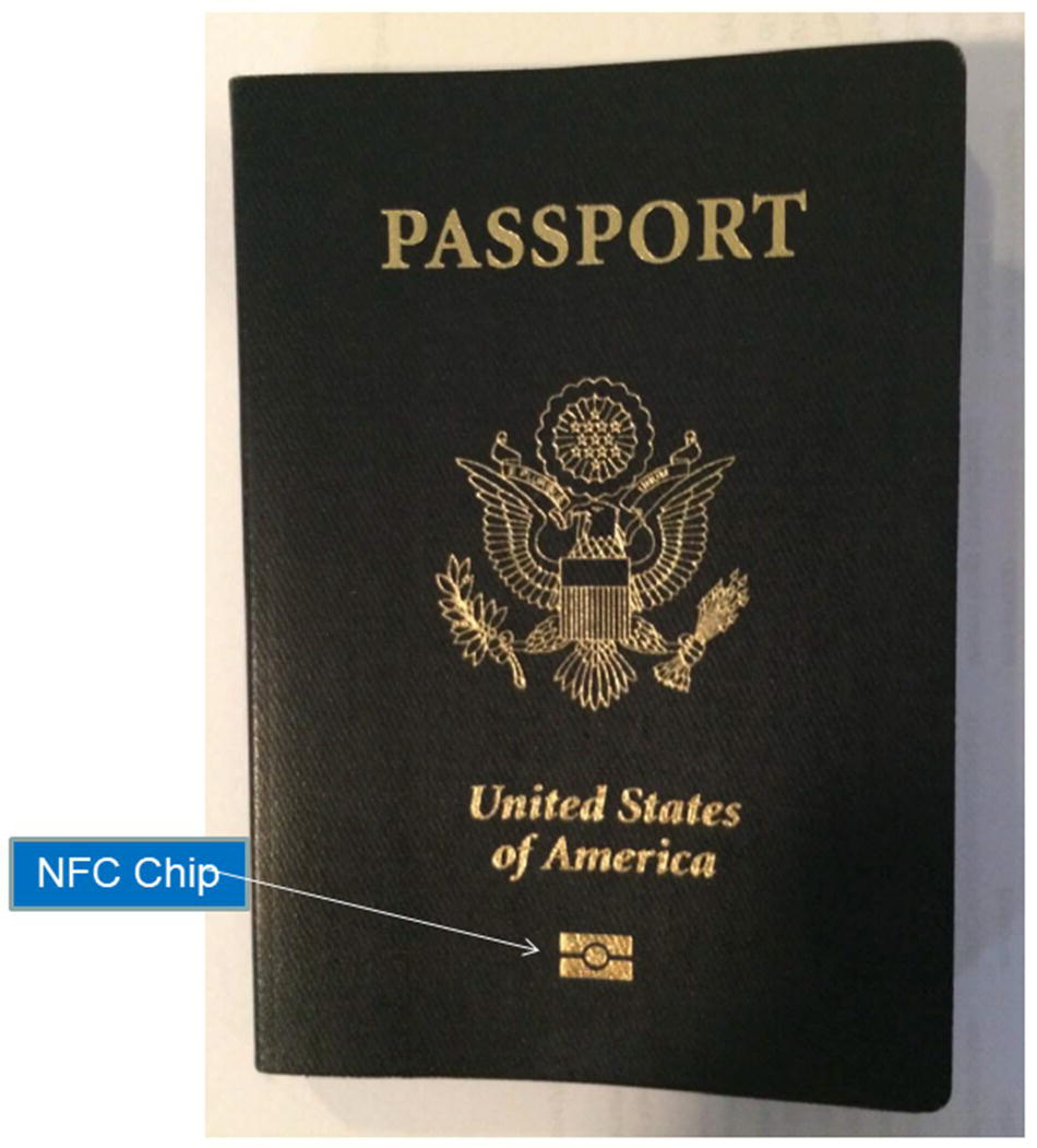
Figure 2.29 Picture of US Passport with the cover closed, with the position of the NFC chip indicated.
Photo by B. Prince.
Tags can either be passive or active. Passive tags collect energy from an interrogating reader interface while active tags have a local power source. An example of an NFC tag family was introduced in February of 2016 by NXP for smart home applications. These tags combined a passive NFC interface and a contact I2C interface together with a nonvolatile memory [37]. This tag offered zero power capability along with password protection, full memory access from both interfaces, and an originality signature for protection against cloning. This second generation part had four times the data transfer performance of the first generation along with backward compatibility to earlier generations. It had a pass‐through mode with a 64‐byte SRAM buffer, a 1912 bit EEPROM user memory, 32‐bit password protection, NFC Type 2 tag, and a 7B serial number. An originality signature was based on elliptic curve cryptography for authentication. It used energy harvesting from the NFC field to power external devices. The operating temperature range was –40 to +105 °C.
2.6.3 Bluetooth‐Based Beacons and Sensor Nodes
Bluetooth is a standard protocol for securely transmitting data using a 2.4 GHz wireless link. It is used for short range, low power, and low cost wireless transmission between electronic devices. Standard Bluetooth has a range of 1–100 meters with a point‐to‐point topology while Bluetooth Smart has a range of 10–100 meters with a point‐to‐point star topology. Bluetooth can be used for smart retail beacons, which can recognize a nearby shopper’s mobile device and transmit information to the targeted shopper. See Figure 2.30 for an illustration of a shopper with a smart phone interacting with a retail beacon.
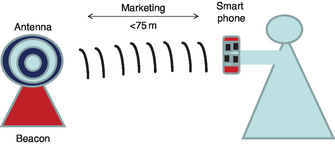
Figure 2.30 Illustration of retail beacon interacting with individual shopper’s smartphone.
These beacons can be preprogrammed to respond to particular user profiles. Macy’s department stores are reported to have implemented Bluetooth beacons [38]. In September of 2014, they reported expanded use of low energy beacons to include several departments in all stores. These beacons enabled a shopper, who elected to be in the system, to receive discount coupons and rewards while they were in a store based on their location in the store. Another possible application for beacons is in museum exhibits where exhibits can detect the presence of a user and transmit interesting information about nearby exhibits. Criteria for transmission might include a defined transmission range to avoid interference between individual beacons.
An illustration of a chip for a Bluetooth beacon was announced in December of 2014 by EM Microelectronics [39]. This was a coin‐sized beacon consuming less than 25 μA average current that typically provided 12 months operation from a single CR2032 coin battery included in the beacon. The beacon used an EMM ultralow power MCU. The 0.9 V 8‐bit RISC Flash MCU contained from 5 KB to 16 KB of Flash EEPROM and a miniature antenna that made the beacon detectable 75 meters away by an advanced smart phone. Its rugged package made it suitable for outdoor music festivals, sporting events, and arenas.
An early low energy Bluetooth compatible chip was introduced by Nordic Semiconductor in June of 2012 [40]. This multiprotocol Bluetooth 2.4 GHz RF Flash‐based SoC was designed as a single chip solution for applications such as fitness and healthcare wearable sensors. It included 256 KB of embedded Flash and 16kB of RAM. Peripherals included: SPI, two‐wire, ADC. The power supply range was 1.8 to 3.6 V. It included a DC/DC converter for 3 V coin cell batteries. A complete Bluetooth protocol stack was included along with 2.4 GHz RF protocols and 128 KB of Flash and 10kB of SRAM were available for an application code.
A Bluetooth Module Add‐on for IoT Designs was introduced in August of 2015 by Silicon Labs. This Bluetooth module was intended to help developers reduce development costs and improve compliance by adding a “plug and play” Bluetooth to their designs [41]. The module provided precertified use in the markets of North America, Europe, and Asia Pacific. The modules were preloaded with the Bluetooth 4.1 compliant software stack and were field upgradable to Bluetooth 4.2 and beyond.
Two Bluetooth ICs that supported Bluetooth Low Energy (LE) ver. 4.1 communications were introduced in November of 2015 by Toshiba [42]. One tag integrated a built‐in Flash ROM and the other supported both Flash ROM and NFC Forum Type 3 Tag for peer‐to‐peer communication. The latter device included a Flash ROM to store user programs and data along with a 64 KB user program area using an internal SRAM to execute various application programs. The chip’s NFC Tag achieved easy Bluetooth peer‐to‐peer pairing and power ON/OFF functions by touching another NFC supported mobile device. The built‐in Flash ROM eliminated any need for an external EEPROM and reduced external part counts and PCB size. The NFC tag was powered by small coin cell batteries.
It was expected that these devices would ease adoption of Bluetooth LE communications for small devices such as wearable healthcare devices, sensors, and toys. Characteristics of a typical Bluetooth LE type 3 Tag are shown in Figure 2.31. Communication was an NFC Type 3 Tag at 212 kbps/424 kbps. Security was mutual recognition by Triple DES Message Authentication code (MAC).
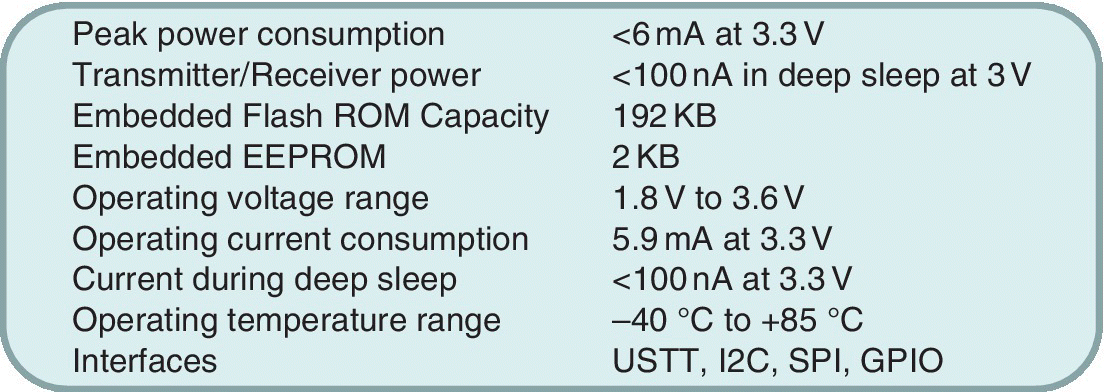
Figure 2.31 Characteristics of a typical Bluetooth LE type3 tag.
Based on Toshiba PR, November 17, 2015 [42].
Bluetooth is being added to applications such as connected home, wearables, remote controls, baby monitors, beacons, electronic shelf labels, audio equipment speakers, health and fitness devices, and point of sale equipment. Figure 2.32 is a photo of a wireless Bluetooth Speaker.

Figure 2.32 Illustration of wireless Bluetooth speaker.
Photo by B. Prince.
In February of 2016, Silicon Labs announced an SoC family intended to support these applications [43]. These Bluetooth SoCs consume 8.7 mA in the peak receive mode and 8.8 mA at 0 dBm in the peak transmit mode and offer –94 dBm sensitivity and output power from –30 dBm to +19.5 dBm. The 40 MHz RISC processor had a powerful floating point and DSP capability. It consumed 63 μA/MHz current in the active mode. An integrated hardware cryptographic accelerator permitted autonomous encryption and decryption of Internet security protocols with minimal CPU intervention.
Another MCU intended for wearables, IoT devices, sensor hubs, building automation, personal medical devices, and smartphones was introduced in December of 2015 by STMicroelectronics [44]. This MCU included an RISC core performing at 125 DMIPS and 339 EEMBC CoreMark at 100 MHz. The accelerator helped drive dynamic power down to 89 μA/MHz with STOP current of 6 μA. Communication includes NFC, Bluetooth, or IEEE 802.15.4 radio boards. The devices have from 64 KB to 128 KB of Flash and 32 KB of SRAM. A RUN mode permits the Flash to be powered down for power savings. To save power, sensor data could be captured directly into SRAM while the CPU and Flash remained off. It had six timers including motor control and 32‐bit/100 MHz timers. Communication ports included: SPI, I2C, I2S, USART, and ISO7816 interface along with a 12‐bit DAC.
2.6.4 IoT Devices with Wi‐Fi
A Wi‐Fi platform can be designed to help add ultralow power long range connectivity to IoT designs. Wi‐Fi is supported by laptops, smart phones, tablets, and other connected things, making it useful for device‐to‐cloud or device‐to‐device connectivity. In November of 2015, TI discussed an ultralow power Wi‐Fi platform using a sub‐1 GHz wireless MCU [45]. This wireless MCU offered 20 years of battery life for applications such as: building and factory automation, alarm and security, smart grid, and wireless sensor networks. The chip had an integrated RISC MCU sensor controller, low power modes, and 0.6 μA sleep current. The wireless sensitivity spanned from full building to citywide coverage for over 20 km on a coin cell battery with up to 128 KB of embedded Flash possible. The wireless MCU operated in various ISM bands. Communication protocols included: Bluetooth, Wi‐Fi, Zigbee, and others.
A plug and play Wi‐Fi module for use with Internet of Things (IoT) applications was discussed in February of 2016 by Silicon Labs [46]. The module had good RF performance, a small footprint, easy application development, and fast time to market. It included: a 2.4 GHz 802.11 radio, integrated antenna, global certifications, an MCU, an embedded Wi‐Fi stack, and various Internet protocols. By integrating the 802.11 radio, antenna, MCU and Wi‐Fi stack the module helped reduce development risk and accelerate the time to market. The module was useful for adding Wi‐Fi to industrial M2M systems, wireless sensors, remote controls, thermostats, connected home products, automotive infotainment, point‐of‐sale devices, and fitness and medical equipment. The module included a scripting language to develop and host end applications. It could run in a network co‐processor mode, enabling the host controller to handle applications tasks. The module enabled connectivity up to 300 m to 500 m typically and had a 2.4 GHz transceiver and an integrated high efficiency chip antenna along with peripherals including: UART, I2C, SPI, and USB. A Wi‐Fi protocol stack included protocols for cloud integration. A dedicated host interface was provided to external MCUs running the end application.
A wireless Wi‐Fi router is a device that performs the functions of a router and also those of a wireless access point. It can provide access to the Internet or to a private computer network. An office Wi‐Fi router is shown in Figure 2.33.
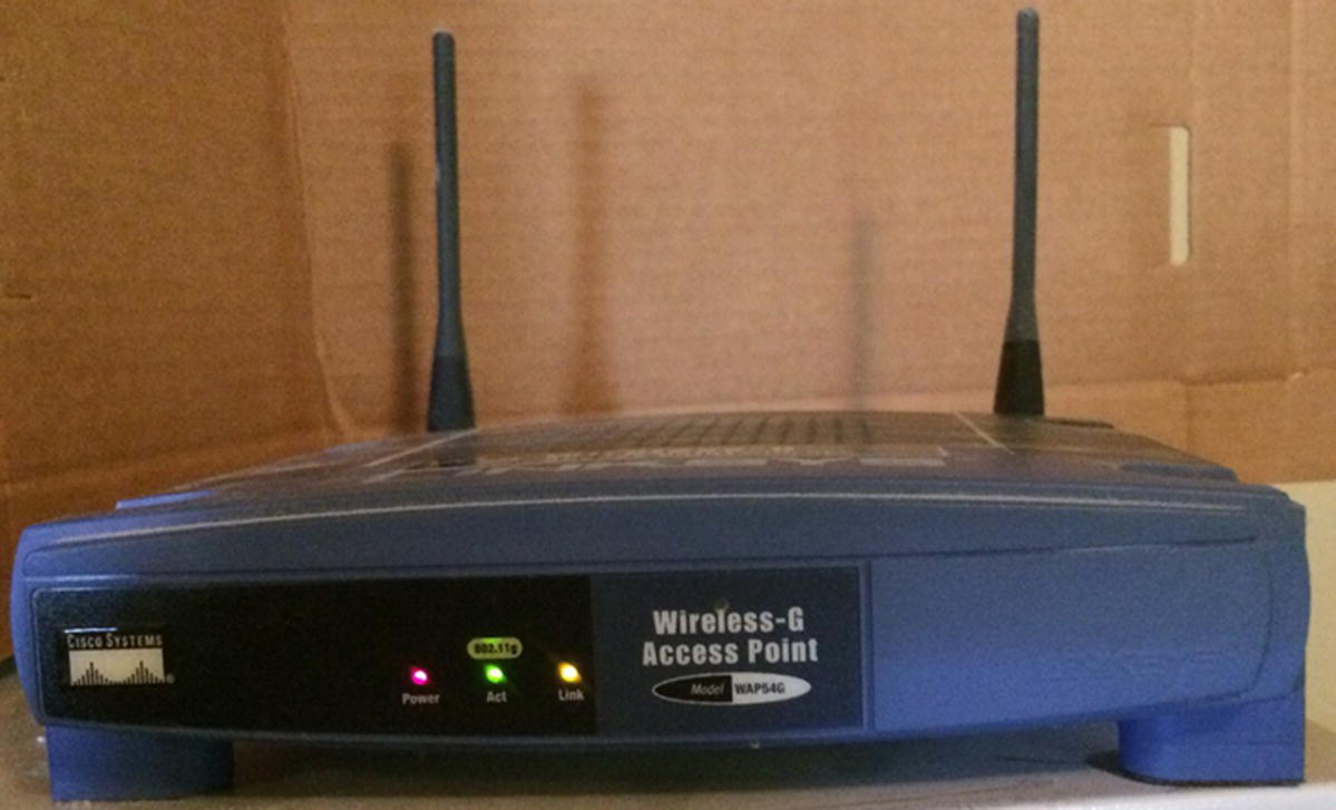
Figure 2.33 Office Wi‐Fi router used in the offices at Memory Strategies International.
Photo by B. Prince.
In February of 2016, Silicon Labs discussed a wireless SoC with embedded Flash [47]. The wireless SoC integrated an RISC processor, a 2.4 GHz radio with up to 19.5 dBm output power, and hardware cryptography. The design included Thread and Zigbee stacks for mesh networks, intuitive radio interface software for proprietary protocols, Bluetooth for point‐to‐point connectivity, and tools to simplify wireless development, configuration, debugging, and low energy design. The wireless portfolio included three options for multiprotocol SoCs optimized for IoT: one had wide output power and range, one had Zigbee and Thread connectivity for mesh networks, and one offered flexible proprietary wireless protocol options for different applications.
The wireless SoCs had a multiprotocol 2.4 GHz RF transceiver in a single chip with up to 256 KB of Flash and up to 32 KB of RAM. Energy modes included: fast wake‐up sleep transitions, a system that enabled autonomous operation of low power peripherals while the MCU core slept. The MCU included floating point capability and consumed 63 μA/MHz in active mode. It integrated a software programmable power amplifier and provided a scalable output power, which ranged from –30 dBm up to +19.5 dBm for applications requiring long range connectivity.
For security, the device had a built‐in hardware cryptographic accelerator, which provided fast, energy efficient autonomous encryption and decryption of Internet security protocols with minimal CPU intervention. The on‐chip accelerator supported algorithms such as AES with 128‐bit or 256‐bit keys, elliptical curve cryptography, and the secure hash algorithm (SHA)‐1 and its follow‐on SHA‐224/256. The hardware cryptography enabled developers to meet evolving IoT security requirements more efficiently than software only techniques.
2.6.5 IoT Devices with USB Connectivity
The Universal Serial Bus (USB) interface is a fast serial bus technology that permits an electronic device to be connected to a computer. USB Flash drives are Flash memory for data storage with a built‐in USB interface. Introduced in 1996, it was intended that all USB ports supply 5 V. USB2 could pull up to 100 mA while USB3 could draw from 150 mA to 900 mA.
An MCU was introduced in May of 2015 by Silicon Labs that enabled USB connectivity for a range of IoT applications including: smart metering, home and building automation, alarm and security systems, smart accessories, and wearable devices [48]. This 32‐bit MCU was based on a RISC core, low energy peripherals, and a range of memory options. It had an energy management system with five energy modes ranging from active mode to deep sleep mode. In deep sleep mode the MCU had 0.9 μA standby current with a 32.8 kHz RTC, RAM/CPU state retention, brown out detector, and power‐on‐reset circuitry active. Active power consumption dropped to 130 μA/MHz at 24 MHz with read word code using a prime number algorithm. There was a 2 μs wake‐up time from standby mode. On‐chip peripherals included: analog comparator, supply voltage comparator, on‐chip temperature sensor, programmable current DAC (IDAC), and a 12‐bit ADC with 350 μA current consumption at a 1 MHz sample rate. On‐chip AES encryption permitted secure wireless connectivity for IoT applications such as smart meters and wireless sensor networks. The chip eliminated many discrete devices by using a full‐speed USB PHY, an on‐chip regulator, and resistors.
IoT devices with USB connectivity for applications such as remote controls and thermostats have been introduced. In February of 2016, Silicon Labs introduced its 8‐bit MCU portfolio for IoT, which included low power capacitive touch control and USB connectivity [49]. One such MCU had speeds of up to 48 MHz and 8–64 KB Flash sizes and can be used for higher end personal medical devices, remote controls, and thermostats. These have a high precision internal oscillator, a clock recovery circuit, a full speed USB transceiver, along with an on‐chip battery charger detection module.
2.6.6 Single Wire Connectivity
Single wire connectivity has the advantage of minimizing the pins on the package to reduce the size of the package. In August of 2015, Atmel introduced a 2‐pin, self‐powered single‐wire serial EEPROM for the IoT and other markets [50]. The part was self‐powered by a parasitic power method over the data pin. It required just one data and one ground pin, which eliminated the requirement for external power. It had a plug and play 64‐bit serial number for identification. The device’s ultralow power requirements included a standby current of 700 nA, write current of 200 μA, and read current of 80 μA at 25 °C. The power scheme eliminated the need for external capacitors and rectifiers. The device had a high write endurance capability permitting more than one million cycles per memory bit. This device was targeted at IoT applications including wearables such as smart fitness and healthcare devices and consumables.
The devices followed the I2C protocol, which allows low overhead migration from existing EEPROMS and the capability of connecting up to eight devices on the same bus. The part had a security register with a 64‐bit factory programmed serial number and an extra 16‐bytes of user programmable and permanently lockable EEPROM storage for a unique serial number for inventory tracking and asset tagging. The data could be permanently protected. Different low voltage battery requirements were supported including low voltage applications at 1.7–3.6 V and 2.7–4.5 V for use with Li‐ion polymer batteries.
2.6.7 Zigbee Interface
Zigbee is a standard interface with a mesh topology and a range of 10–100 meters. Its maximum datarate is 250 kbit/s at 2.4 GHz [51]. It is intended as a communications protocol for creating personal area networks with low power digital radios for applications such as home automation and medical device data collection. It is a low power, low data rate, close proximity, personal area wireless network that is intended to be simpler than Bluetooth or Wi‐Fi.
2.6.8 ANT Interface
ANT is a proprietary interface with a range of 30 meters at 0 dB m. It is an adaptive isochronous network technology that ensures coexistence with other ANT devices. Each transmission occurs in an interference free time slot within the defined frequency band. Transmission is for less than 150 μs per message, which permits a single channel to be divided into numerous time slots [52].
2.7 Wearable Medical Devices
2.7.1 Overview of Wearable Medical Devices
Portable medical systems are a growing market due to the increasing proportion of Seniors in the population worldwide. These portable systems require large high performance memory but must have low power for battery operation. The wearable electronics part of this application includes devices for medical, fitness, and wellness, such as step tracking, heart rate and blood pressure monitors, blood glucose monitors, insulin pumps, hearing aids, and other. To service this application, suppliers of smart connected wearable devices will require low power platforms with simple basic features that include: a simple user interface, embedded processing for data collection, and sensors for environmental tracking. The portable medical system application also includes devices such as: miniature medical sensors, portable datalogging equipment, medical and pharmaceutical tracking, and implantable medical devices such as defibulators and pacemakers. Figure 2.34 is an illustration of a wireless network of wearable medical devices.

Figure 2.34 Wireless network of medical devices to medical suppliers and monitors.
Portable medical devices are expected to use embedded EEPROMS and Flash memory as well as fast access, low power nonvolatile emerging memories such as FeRAMs, Conductive Bridge (CB) RAMS, and MRAMs. Powering these devices will require either long term batteries or energy harvesting systems. These devices will need to be networked to medical surveillance systems and medical personnel requiring networks of IoT communication devices.
These portable networked medical devices are expected to be used increasingly by the aging population, which the United Nations estimates today at 900 million including 250 million in developed countries and another 650 million in developing countries [53]. This total is expected to grow to 1.2 billion by 2025. With medical care improving worldwide, these higher value portable medical and tracking devices could provide another large market for fast, low power nonvolatile memories.
2.7.2 Miniature Hearing Aids Using FeRAM Memory
The fast write speed and low power consumption during write of the 1T1C FeRAM memories compared to EEPROMs made them an obvious choice for use in battery powered medical devices such as hearing aids. In March of 2013, Fujitsu America introduced 1 Mb and 2 Mb FeRAM memories [54]. These parts were intended for miniature medical devices where the faster write speed than EEPROM eliminated undesirable noise. They consumed 92% less power during write than similar capacity EEPROMS and had a 920 times faster write speed. Endurance was >1012 write cycles for prolonged battery life. In a system, this single chip solution reduced: component count, the size of the battery, cost, footprint, and power consumption compared to memory solutions using EEPROM or SRAM plus a battery. The fast random access of the nonvolatile FeRAM permitted more data to be retained when the power is switched off’
2.7.3 Body Sensor Node Platforms Using CB‐RAM Memory
Body sensor node (BSN) networks need to operate from low levels of harvested power without a battery in the system. Low operating power nonvolatile memory is essential for the long term operation of these systems. In June of 2013, Adesto and the University of Virginia discussed a CB‐RAM macro that was embedded in a BSN processing platform [55]. The device operated at voltages as low as 600 mV for write and 300 mV for read. This enabled low energy operation and compatibility with low energy digital systems. The charge pumps required for EEPROMs were eliminated. The memory macro permitted a 100 times reduction in write energy compared to Flash memory and write operation down to 0.6 V, which is compatible with other ultralow power SoCs used in wireless body sensor networks. Wireless nodes and body sensors are expected to operate at 1 V and below.
Two CB‐RAM macros were embedded in a subthreshold voltage operating SoC, which provided a digital platform for body sensor nodes to process ECG, EEG, and EMG signals. The architecture included a programmable RISC processor, a custom node controller, DMA and accelerators for heart‐rate extraction, and atrial fibrillation detection. The CB‐RAMs acted as instruction and data memories. The chip was found to execute properly after a day of power‐down. This confirmed the nonvolatile storage and operation of the low voltage arrays. An illustration of the die showing the two 64Kb macros integrated with the BSN digital platform is shown in Figure 2.35.
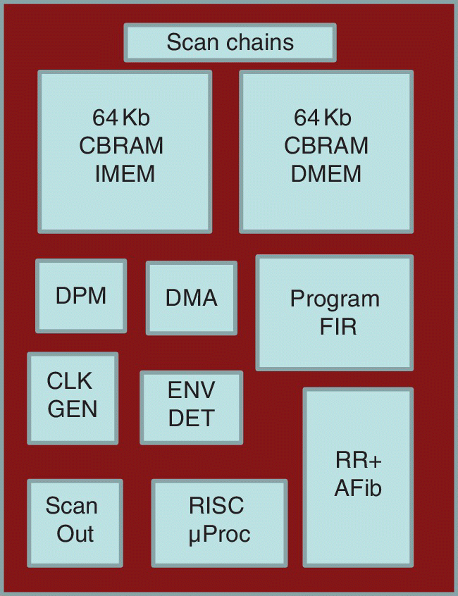
Figure 2.35 Illustration of die layout showing two 64Kb CBRAM macros integrated with the Body Sensor Node (BSN) digital platform.
Based on N. Gilbert et al. (Adesto, University of Virginia), VLSI Circuits Symposium, June 2013 [55].
2.7.4 “Store Mostly” Healthcare Systems Using MRAM
An STT‐MRAM can use less energy than a comparable SRAM in a system if the memory bandwidth utilization is low. In November of 2013, Kobe University and LEAP discussed a 65 nm single supply voltage 8 Mb STT‐MRAM with a process‐variation tolerant sense amplifier that could be used for minimal energy SRAM replacement in an infrequent access platform such as a healthcare system [56]. The sense amplifier used a boosted gate NMOS and negative resistance PMOS as loads. These maximized the readout margin in all process corners.
The STT‐MRAM achieved a cycle time of 1.9 μs (0.526 MHz) at 0.38 V. The operating power was 6.15 μW at 0.38 V and the minimum energy per access was 3.89 pJ/bit at VDD = 0.44 V. The characteristics of the 65 nm CMOS test chip included: a nominal voltage of 1.2 V, operating VDD from 0.38 to 0.6 V, and operating frequency of 0.526–5000 MHz.
The STT‐MRAM was found to use less energy than a comparable SRAM if utilization of the memory bandwidth is 14% or less, which means the STT‐MRAM is preferable in less active applications such as a healthcare system or a sensor network. If, however, the energy consumption of the proposed STT‐MRAM and an LV SRAM are compared and the ratio of read and write access is 50:50 at an operating voltage of 0.5 V, the energy consumed in the STT‐MRAM is 3.03 times larger than in the SRAM. The STT‐MRAM cell size was 0.203 mm2, which compares favorably with the SRAM cell size in that technology.
2.7.5 Wearable Biomonitoring with NFC and eFeRAM Memory
A low power wearable biosignal monitoring system that communicated with smart phones using Near Field Communications (NFC) was discussed in June of 2013 by Kobe University and Omron Healthcare [57]. The NFC was used to check vital signs easily at any time using the smart phone. The system included: a battery, electrodes, a triaxial accelerometer IC, an NFC tag IC, and a biosignal processor LSI with embedded FeRAM.
The biosignal processor LSI was made in 130 nm CMOS. It included: heart‐rate monitoring circuits, a 32 KB ferroelectric RAM, an accelerometer interface, and an NFC interface. This system used 38.1 μA of power for the logging application running at 320 kHz with a 3.0 V power supply.
The goal of this system was mobile wellness achieved by daily life monitoring of vital signals and physical activity of elderly people. This wearable system could log instantaneous heart rate and acceleration, along with physical activity and estimation of exercise intensity. The key factors affecting usability were miniaturization and weight reduction. Battery mass and power consumption reduction were critical. A block diagram of the biosignal processor LSI showing the embedded 32 KB data FeRAM is shown in Figure 2.36.
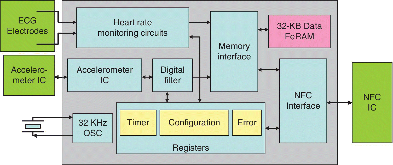
Figure 2.36 Schematic block diagram of a biosignal processor LSI.
Based on K. Yamashita et al. (Kobe University, Omron Healthcare), NEWCAS, June 2013 [57].
While a wireless transceiver consumed the most power in the system, the standby power of NFC is small compared to Bluetooth or ZigBee. NFC enabled communication to be initiated without manually configuring the communication link. NFC has high security due to its short communication range.
2.7.6 Wearable Healthcare System with ECG Processor Using FeRAM
An ECG processor intended for use with a wearable healthcare system was discussed in September of 2013 by Kobe University, Rohm, Omron, and JST CREST [58]. The wearable healthcare system included: a battery, an ECG processor, an accelerometer IC, an antenna for near field communications (NFC), and an NFC Tag IC, as shown in Figure 2.37. The system can be accessed by a smart phone or other electronic reader/writer using NFC to handshake with the smart phone.

Figure 2.37 Wearable healthcare system including ECG processor, accelerometer IC, antenna for NFC, and an NFC tag IC.
Based on S. Izumi et al. (Kobe University, Rohm Co., Omron, JST CREST), ISCDG, September 2013 [58].
Key factors affecting wearable system usability include: miniaturization and weight reduction. Noise can affect a wearable electrocardiograph (ECG) monitor since its electrodes are close together. An analog front end is required to counteract noise when the user is active. Battery capacity is related to battery weight, which in turn is affected by the power consumption of the system. If power consumption is low, then battery weight can be reduced. NFC has very low standby power compared with Bluetooth or ZigBee. Active communication energy is consumed by a reader/writer when using a passive NFC tag.
The ECG processor included: an analog front end, a 12‐bit ADC, an instantaneous heart‐rate monitor (IHR), a 32‐bit RISC processor core, and a 64 KB FeRAM. A block diagram of a sketch of the chip photograph for the ECG Processor is shown in Figure 2.38. The chip used 130 nm CMOS technology. Macros included: 2 V digital 64 KB SRAM and 3.0 V 64 KB FeRAM with an area of 0.9 mm. MCU frequency was 24 MHz. The other blocks ran at 32 kHz. The ADC had 12 bit resolution. The total chip current was 12.7 μA for heart‐rate logging.
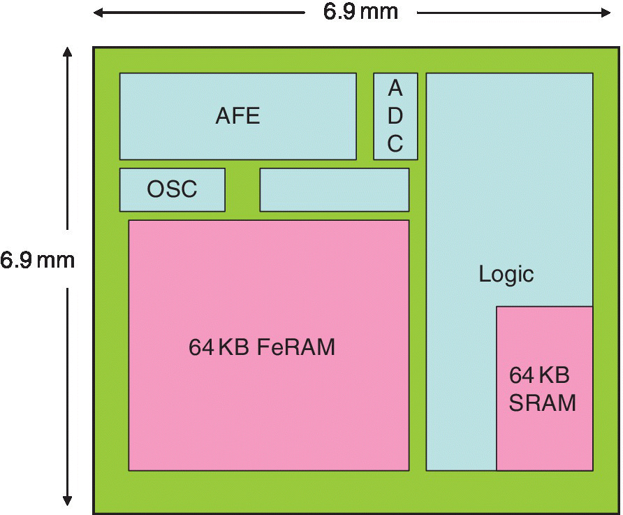
Figure 2.38 Sketch of the ECG processor chip showing 64KB FeRAM.
Based on S. Izumi et al. (Kobe University, Rohm Co., Omron, JST CREST), ISCDG, September 2013 [58].
The heart‐rate monitor used a short term autocorrelation algorithm to improve the heart‐rate detection accuracy in spite of being used in noisy conditions. The instantaneous heart rate is an important biosignal used for heart disease detection, heart‐rate variation analysis, and exercise intensity estimation. The ECG processor chip consumes 13.7 μA for the heart‐rate logging application. A block diagram of the ECG processor is shown in Figure 2.39. The data buffer with a 64 KB FeRAM is shown. In November of 2014, Kobe University, Rohm, and Omron discussed further on this wearable healthcare system with a noise‐tolerant ECG processor with an embedded 64 KB FeRAM data buffer [59]. Wearable systems have size and weight constraints that limit the battery capacity and the signal‐to‐noise ratio of the biosignals.
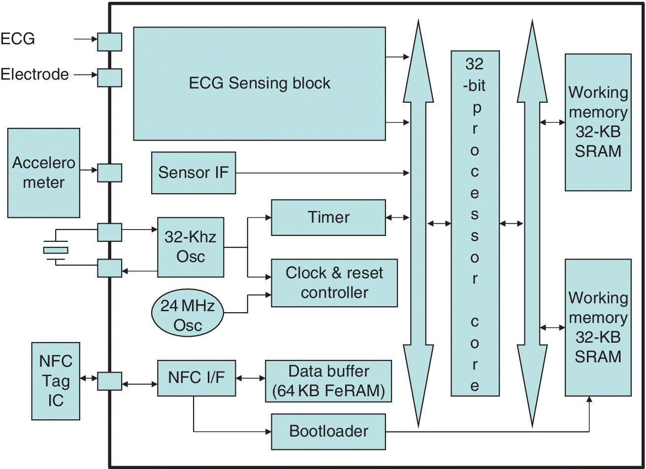
Figure 2.39 Block diagram of an ECG processor with 64KB FeRAM.
Based on S. Izumi et al. (Kobe University, Rohm Co., Omron), IEEE Trans. on Biomedical Circuits and Systems, November 2014 [59].
In January of 2014, Kobe and Rohm discussed “normally off” technologies for healthcare appliances. The application focus was on a daily life monitoring and the ECG processor. The system used an FeRAM and near field communication (NFC) for normally‐off datalogging and data retention. The limitations on wearable system usability are miniaturization and weight reduction [60]. This means battery weight and hence power consumption must be reduced. A wearable biosignal monitoring system using normally off technologies was used to reduce power consumption.
The wearable biosignal monitoring system could acquire long‐term instantaneous heart rate data and an acceleration value. Physical activities were classified using a triaxial accelerometer. The instantaneous heart rate is calculated from the electrocardiogram R‐waves for detection of heart disease, heart‐rate variation analysis, and exercise intensity estimation. To reduce the power consumption, wearable and wireless ECG telemetry system and signal‐chip ECG monitoring system LSIs were developed. The limitations on power consumption and electrode distance on wearable ECG monitors made them sensitive to noise as the subject moves around.
2.8 Low Power Battery Operated Medical Devices and Systems
2.8.1 Overview of Low Power Battery Operated Medical Devices
Portable medical systems are a growing market due to the increasing proportion of Seniors in the population. These require large memory and low power for battery operation. The characteristics of these various portable medical equipment systems are summarized in the table in Figure 2.40.
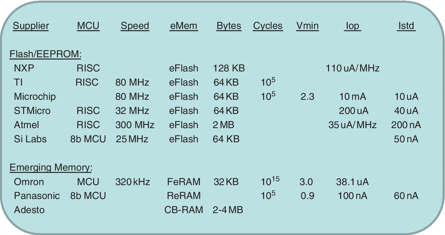
Figure 2.40 Features of various portable health monitor Flash MCU including nonvolatile memory and electrical characteristics.
Currently there are a number of suppliers and developers with Flash MCU for portable health monitors. Details are in the next two sections. Most use RISC processors with embedded EEPROM and eFlash in amounts ranging from 64 to 128 KB of eFlash. Endurance is commonly indicated at 105 cycles. Operating current ranges from 35 to 110 μA/MHz. Standby current ranges from 50 nA to 40 μA. Suppliers and developers with embedded emerging memory targeted at portable health monitors offer embedded FeRAM, RRAM, and CB‐RAM..
2.8.2 Low Power Battery Operated Medical Devices Using eFlash
A significant number of low power battery operated medical devices have been developed in the past few years. Many of these use the embedded Flash memory macros that are already available at various foundries to embed in SoC along with commercially available RISC cores. A number of foundries have also introduced embedded Flash memory macros for low power applications.
A 40 nm low power process with an embedded NVM intended for IoT type applications was announced in March of 2015 by NXP to be run at Global Foundries in Singapore [61]. Volume production on 300 mm wafers was expected in 2016 for this process, which was intended for MCU with embedded Flash memory for applications such as ID, near field communications (NFC) and healthcare.
In September of 2014, TSMC announced an ultralow power (ULP) platform for IoT and wearable devices that included 55 nm, 40 nm, and 28 nm ultralow power processes and offered FinFET ultralow power processes down to 16 nm [62]. RF and eFlash memory were available in 180 to 40 nm ULP technology for IoT. Logic IP and libraries were available in the ULP processes with early designs in processes down to 28 ns node planned in 2015. Integration of radio and eFlash was enabled along with the energy efficient RISC CPUs from ARM Corp. A low power mixed signal design flow was offered from Cadence. Fujitsu indicated an interest in the 28 nm ULP technology platform, while Nordic Semiconductor indicated they had selected the 55 nm ULP process for their ultralow power RF SoCs. Compared with previous low power generations, the TSMC ULP processes were expected to reduce operating voltages by 20 to 30% to lower both active and standby power.
A Flash memory using a single poly 130 nm nonvolatile memory technology embedded in a 65 nm logic process was discussed by Toshiba in July of 2015 [63]. This process, which was to be run at UMC in Taiwan, was intended for the low power IoT market for applications such as wearable and healthcare related equipment. The Silicon Storage Technology third generation split gate embedded Flash in the 65 nm logic process was also being offered by UMC for MCUs, with a resulting power of about 60% of that of conventional double polysilicon stacked embedded Flash. In addition, Bluetooth low energy macros had been developed and were targeted at short range wireless products, including NFC controllers and contactless cards. For lower cost applications, an NVM embedded process using single polysilicon multitime‐programmable (MTP) cells intended to run on the 130 nm logic process would be offered. This process limits the increased process steps in mask pattern lithography of conventional embedded Flash.
A number of chips with embedded Flash memory have been introduced for use in health devices. A chip with USB connectivity for use in health devices such as glucose meters and other applications was introduced in June of 2012 by NXP [64]. This 32‐bit RISC MCU had up to 4 KB of EEPROM, 12 KB of SRAM, and 128 KB of eFlash with 256 bytes of the erase sector. Active power was down to 110 μA/MHz for battery operation. USB 2.0 was included. An illustration of a glucose meter is shown in Figure 2.41.
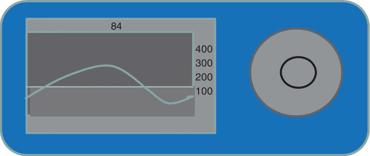
Figure 2.41 Illustration of commercial wearable blood glucose meter.
For health and fitness applications along with consumer and human interface control, TI in September of 2012 announced a kit that permitted engineers to design using an RISC MCU with a floating point operating up to 80 MHz [65]. The MCU included 64 KB of Flash with 105 write/erase cycles, two 12‐bit ADC, and up to 27 timers.
An ionizing radiation sensor with an embedded ultralow power Flash memory was discussed by TowerJazz in November of 2012 [66]. Sensing was accomplished by measuring the accumulated Vt shift of the Flash cell after exposure to radiation. The sensor was intended for inclusion in a passive RFID for radiation measuring systems. It operated at very low power and required no power supply during the exposure sessions.
Devices intended for battery operated accessories and sensors with applications including smart meters and health monitors were introduced in February of 2013 by Microchip Technology [67]. These devices, which offered up to 8 M‐bit of memory, were made using a commercial embedded Flash technology consisting of a split‐gate, NOR embedded Flash with a thick oxide tunneling injector. The parts had an extended operating voltage range from 2.3 to 3.6 V. The memory was partitioned into uniform 4 KB sectors and 32 and 64 KB blocks offering seamless partitioning for program and data code in the same memory block. Sector and block erase was as fast as 18 ms and the entire chip could be erased in 35 ms. Word program time was 7 μs. Endurance was 105 cycles with more than 100 year data retention. The active read current was 10 mA typical at 80 MHz and the standby current was typically10 μA.
For applications that include fitting smaller batteries on portable medical equipment, such as fitness trackers and glucose meters, STMicroelectronics in February of 2014 discussed an ultralow power Flash MCU [68]. The device featured a 32 MHz RISC core, a 100 ksps ADC consuming 40 μA, and a crystal‐less USBFS 2.0 [68]. The ADC consumed 40 μA at 100 ksps up to 200 μA at 1.14 Msps so a coin battery could operate a fitness tracker for two years. The CMOS technology used offered an embedded EEPROM and low variation over the 25 to 125 °C temperature range. Up to 64 KB of Flash memory was included and 2 KB of embedded EEPROM. Figure 2.42 shows a Bluetooth wireless fitness tracker. This fitness bracelet can take heart‐rate readings, track sleep automatically by measuring deep, light, and REM sleep, and has activity tracking. The Bluetooth permits it to communicate with a smartphone.
Figure 2.42 Bluetooth wireless fitness tracker for taking heart rate readings, tracking sleep automatically, and tracking steps.
Photo by B. Prince.
The design of an NFC sensor transponder tag for wearable health and fitness applications was discussed in June of 2015 by Texas Instruments [69]. This tag combined a TI MCU core with an ISO15693 compliant NFC interface for wireless communication. It was optimized to be fully passive without a battery or for a single cell battery mode. It had integrated analog and digital sensor interfaces, which made it adaptable to wearable applications. It could be used to collect data on demand or at regular intervals.
The TomTom Spark GPS fitness watch contained an Atmel smart RISC MCU from ARM with eFlash along with other chips and a software library to control the touch interface, as announced by Atmel in November of 2015 [70]. This ultralow power MCU helped extend the battery life of the fitness watch for up to 10 hours in GPS mode. A smart energy efficient RISC MCU from ARM ran at speeds of up to 300 MHz with up to 2 MB of embedded Flash memory. Features included: USART, SPI, I2C, 12b ADC, and DAC, and a single digital IO (SDIO). This MCU was optimized for applications requiring performance and power efficiency in a small package. Integrated on the chip were: ADC, EEPROM memory, and brown‐out detectors to permit building applications without external components. They also offered Flash memory and on‐chip debug. The chip could operate at 0.7 V.
An application processor intended for use in wearable devices for IoT was announced by Toshiba in September of 2015 with production scheduled for early 2016 [71]. The device could support multiple external sensors and provided a communication environment that made use of the extended hub features of Bluetooth. The device included a Bluetooth v4.1 controller and processor, which can capture data from external sensors connected by various I/Os such as I2C, UART, SPI, and ADC. It also included Flash memory to save data. Both data processing and storing of multiple sensing targets as required for IoT devices were executable simultaneously. The device could also perform as a Bluetooth hub for collecting, processing, and storing data.
The processor has a low power design feature that permits changing the supply voltage with processor frequency. This feature can be used for wearable products that require long operating hours. Software algorithms supported include: activity monitoring and ECG monitoring. This means it provides a total system solution for wearable systems. The communication function, memory, and processor for IoT are integrated in one package.
For next generation wearable IoT devices for battery operated applications that require activity and environment monitoring, Atmel introduced an ultralow power platform in January of 2016 [72]. It included an energy efficient RISC processor from ARM along with an Atmel designed Bluetooth Smart module, which had an active power down to 35 μA/MHz and 200 nA current in sleep mode. It was packaged in a 2.2 mm × 2.1 mm Wafer Level Chipscale Package, which permitted designers to build ultrasmall industrial designs for connected IoT and wearable applications. The entire platform was in a 30 mm × 40 mm form factor, which includes: the MCU, Bluetooth module, capacitive touch interface, security solution, complete software platform, real time OS, a 6‐axis “Smart Hub” motion sensor and a BME280 environmental sensor. The platform could be powered by a simple coin cell battery.
A version of Silicon Lab’s 8‐bit MCU portfolio for IoT intended for personal medical devices and wearables was introduced in February of 2016 [73]. It included low power capacitive touch control and USB connectivity. The low energy 8‐bit device offered a sleep mode power of 50 nA with full memory retention and brown‐out detection, and a 2 μs wake‐up time. Core speeds scaled up to 25 MHz and Flash memory sizes ranged from 2 to 64 KB. It included an on‐chip battery charger detection module. The device is intended for adding USB connectivity to personal medical devices and wearables.
A wrist monitor to track physical activity, sleep quality, breathing patterns, and stress levels and offer actionable suggestions for self‐improvement was discussed in August of 2016 by Nordic Semiconductor [74, 75], The device used a low energy SoC, which automatically synched to a smart phone using Bluetooth wireless connectivity. The 32‐bit RISC core chip from ARM ran at 64 MHz with a 2.4 GHz multiprotocol Bluetooth 4.2 ANT radio with –96 dB RX sensitivity. It had 512 KB of embedded Flash memory and 64 KB of SRAM. It supported up to 5 days of continuous biometric sensing and reconnection between recharges of the Li ion battery. The 2.4 GHz radio had 5.5 mA peak RX/TX current and a fully automatic power management system offering 90 CoreMark/mA. It also had an on‐chip NFC tag for “touch‐to‐pair” communications.
2.8.3 LP Battery Operated Medical Devices Using Embedded Emerging Memories
Low power battery operated medical devices have also been developed using embedded memories of the emerging memory type, such as: RRAM and CB‐RAM. A line of 8‐bit MCU with embedded RRAM replacing Flash memory began production at Panasonic in August of 2013 [76]. Target applications were those that require low power operation such as sensors and portable healthcare devices. The RRAM used Ta2O5 to control oxide density and defects during deposition of the tantalum layer. Uniformity was obtained in the filaments by keeping the electric current constant during the forming process, which resulted in the filaments being uniform. Uniform filaments ensured stable operation. By optimizing the current, the level of filament reduction during the write operation was maximized to assure data retention. The MCU with the embedded RRAM operated at voltages as low as 0.9 V, which permitted low power consumption. The standby current was 60 nA with a 3 V power supply and the operating current was 200 nA during real time clock operation. Compared to a comparable MCU with eFlash, the power consumption was about half. In a comparable eFlash MCU, the write voltage was 2.7 V and the write speed was 30 μs/byte, while in the MCU with eRRAM, the write voltage was 1.8 V and the write speed was 3 μs/V. The rewrite cycle endurance was 100 000. The RRAM was being installed in the back‐end process so it would be usable in various process nodes. The RRAM characteristics are shown in Figure 2.43.
Figure 2.43 Features of Flash MCU with embedded RRAM for low power battery operated portable medical devices.
Based on Semiconductor Industry News, August 22, 2013 [76].
In October of 2013, Adesto Technologies and Nordion, who make commercial gamma irradiation systems, discussed the Gamma irradiation tolerance of the Adesto CB‐RAM nonvolatile memory [77]. The tests exposed standard packaged CB‐RAM to doses up to 5 Mrad and showed the immunity of CB‐RAM to gamma radiation. The results open medical applications, and other uses that require sterile memory components, to CB‐RAM technology, since gamma irradiation is a conventional method of sterilization of single use medical devices from microbial decontamination.
A family of sterilization‐tolerant low energy CB‐RAM products was announced by Adesto in August of 2014 for wearable medical devices [78]. These devices have been shown to maintain data during high temperature and irradiation conditions of the sterilization processes used in medical device manufacturing. Applications include: wearable electronics, orthopedics, smart syringes, smart sample containers, and surgical devices as well as in application areas such as RFID biomaterial tracking, drug delivery, and capsule endoscopy.
A line of 1.65–4.4 V serial Flash memories using conductive bridge RAM (CBRAM) technology targeted for use in Internet of Things (IoT) applications was announced by Adesto in November of 2015 [79]. The memory was offered up to 4 Mb densities and could be used with wearable wireless sensors. It has deep power down, active interrupt, and an extended voltage range. It can be used with lithium polymer battery chemistries without added circuits. In February of 2016, Adesto described the power consumption of a CBRAM chip using an SPI interface made in a 130 nm process [80]. Core voltage is 1 V and write is at 2.5 V. Power consumption is low enough that a small capacitor can provide enough energy to write 32 bytes of data into the CBRAM. Reading 500Kb/s of data consumes 10 μW or 10 pJ/bit.
2.8.4 Security for Medical Systems
Security is essential for workable IoT applications and in particular for chips intended for medical systems. Hardware security on MCUs with an embedded Flash memory is expected to be able to meet the need for secure applications in areas such as payment applications and wearable devices.
A family of very low power MCUs was described in August of 2015 by Microchip Technology, which included an integrated hardware crypto engine with both OTP and RAM options for secure key storage and up to 256 KB of Flash memory [81]. It also included a direct drive for segmented LCD displays. A dual partition Flash with live update capability permitted the device to hold two independent software applications. It also permitted simultaneous programming of one partition while executing the application code from the other. This feature is thought to make the chip suitable for applications that require secure data transfer and storage and long battery life, such as industrial and medical applications.
A family of secure MCU was introduced in November of 2015 by STMicroelectronics. These devices included up to 2 MB of 40 nm embedded Flash program memory, fast clock speed, and a fast embedded cryptographic accelerator based on a 32‐bit secure core processor from ARM [82]. The hardware architecture provided multiple strong fault protection mechanisms for CPU, memory, and buses for secure software and systems. It was expected to meet the need for secure applications in areas such as payment applications and wearable consumer devices as well as in machine‐to‐machine communications in factory automation and automotive in‐car communications. The peripheral had a secure Data Encryption Standard algorithm and a cryptoprocessor that supported the public key algorithm. The inclusion of 2 MB of eFlash permitted the device to host additional applications.
In October of 2013, the Institute for High Performance Microelectronics (IHP) described a sensor node crypto‐processor for use in wireless sensor networks with strong security requirements [83]. Wireless sensor networks consist of several randomly deployed sensor nodes that rely on very limited power resources. The SoC used was a mixed signal processor with hardware crypto‐accelerators for secure communication in the network. The system architecture combined an asynchronous processor core with a synchronous peripheral, which resulted in low power system operation. The chip integrated a 12‐bit ADC and a 64KB sector embedded Flash on the chip. The improved security of the system was at the cost of an additional chip area and increased standby power. A digitally controlled oscillator was expected to be later included as an option to reduce the total power of the chip.
An MCU that combined a hardware cryptography engine, low energy modes, on‐chip DC–DC converter and scalable memory for IoT applications such as wearable health and fitness devices was announced in December of 2015 by Silicon Labs [84]. The MCU addressed the need to equip IoT connected devices with security technology. The cryptography engines provided autonomous encryption and decryption for Internet security protocols such as TSL/SSL with minimal CPU intervention. The crypto‐accelerator supported algorithms such as AES with 128‐bit or 256‐bit keys and elliptical curve cryptography. The hardware cryptography was found to meet evolving IoT security requirements more efficiently than software only techniques. These MCUs had an enhanced peripheral reflex system that allows low power peripherals to operate autonomously while the MCU core sleeps. This permitted connected devices to sleep longer and it extended battery life. The active mode current was 63 μA/MHz and sleep mode current ranged from 1.4 μA down to 30 nA. Ultrafast wake‐up/sleep transitions minimized energy consumption. The MCU integrated a high efficiency on‐chip DC–DC buck converter with current capacity of 200 mA, which provided a power rail for other system components while also powering the MCU. Scalable memory options included up to 256KB Flash and 32KB SRAM.
2.9 Automotive Network Applications
2.9.1 Overview of the Automotive Application
Automotive remains one of the largest Flash MCU applications. Embedded Flash memory size is growing with a more complex application code for increased functionality along with the potential to be customized for personal preferences. In automotive applications, for example, dynamic driver modes may let a driver select between Economy, Comfort, or Sport driving modes, which requires increased storage capacity in the powertrain MCU managing the engine.
Another factor increasing the complexity of applications like automotive are the requirements that different subsystems be able to share information to make better real time decisions. The evolution of Advanced Driver Assistance Systems (ADAS) is an example of this concept. The interlinking of different subsystems within a car is driving the requirement for more Flash memory in the controlling MCU. The need for datalogging is also rapidly increasing the amount of embedded Flash memory in the car. Information like odometer readings, critical sensor readings, crash logs and black box machine states are immediately written into data Flash when power is lost or crash events occur. The serviceable lifespan of a car is approaching 15–20 years and EEPROM data sets stored in data Flash are requiring 500 000 or more updates. This means that 512 KB or more of high endurance data Flash is required. A high performance automotive powertrain MCU has high bandwidth Flash memories to meet the demanding engine control applications. Embedded 28 nm Flash products are expected to enable 16 to 32 MB of Flash to be integrated into automotive MCU in support of powertrain and ADAS solutions.
Flash MCUs with embedded Flash memory are essential in automotive applications for complicated real time controls for higher fuel efficiency, better safety, and increased connectivity. High density, fast random read access is needed from the eFlash. The requirements for eFlash in automotive are secured operations and data reliability in particular reliable program/erase cycling at high temperature. Automotive has stringent operational, environmental, and reliability requirements.
Automotive ICs made after 2016 by Global Foundries are expected to include faster processors based on 22 nm FD‐SOI, eMRAM and 5G wireless communications [85]. For advanced driver assistance systems (ADAS), cars will need to have up to five cameras per car and the image processors must be fast enough to react instantaneously to objects in the path of the car. GlobalFoundries expected FD‐SOI technology to improve the linearity and insertion loss of RF circuits. Automotive MCUs for under‐the‐hood applications must operate reliably at 125 to 150 °C ambient with an even higher junction temperature. Under‐the‐hood applications include: powertrain, body, and safety systems. These high temperatures result in leakage being about 30% of total power for 55 nm bulk silicon technology since, in CMOS, leakage increases exponentially with temperature, whereas in 22 nm FD‐SOI leakage is decreased and the technology is shrunk. High‐k dielectrics will be required for automotive technology at the 28 or 22 nm rather than the replacement gate or gate last techniques used in other foundries. For in‐cabin systems, such as infotainment, the temperature requirement is lower. Some examples of Flash MCU for various recently announced automotive applications are shown in Figure 2.44 along with the type of MCU and the amount of Flash expected to be embedded in the MCU. These and other examples of automotive Flash MCU are discussed in this section.
Figure 2.44 Examples of automotive applications, typical MCU, typical embedded NVM capacity for applications, and types of embedded nonvolatile memories used in these applications.
More detailed descriptions of various Flash microcontrollers that have been recently introduced for automotive applications are shown in the rest of this section as an indication of the characteristics of this application. Electronic control systems for automotive have meant that many Flash MCUs have been used in automobiles. Embedded Flash memories are used for control program code storage and for temporary data storage to provide flexibility for program update and improved control.
Requirements for automotive eFlash were discussed by Renesas in January of 2016 [86]. These included: operating and data retention junction temperature up to 170 °C for under‐the‐hood applications and random read access throughput, particularly for high end Flash MCU. Over 100 MHz random read access frequency is needed to achieve real time engine controls for higher fuel efficiency and for advanced driver assistance systems (ADAS). This means that fast error corrected throughput for the Flash memory is needed for advanced automotive applications. Since ECC and parity check slow down the operation, they are not applicable. This higher data reliability needs to be achieved by the memory cell itself and by very accurate read out circuits. In addition, the requirement for high speed data processing in automotive Flash MCU has required the integration of high speed CMOS logic circuits and embedded Flash and it is important to balance sufficient performance of the logic CMOS transistors and the memory cell reliability.
ADAS systems in autos include: multiple all around cameras and radar systems. An example of a car with radar systems is shown in Figure 2.45 [87]. These ultrasonic systems could be used for ultrasonic parking assist and blind spot detection. Automated radar sensors could be used for cross traffic alert, lane change assist, backup aid, side impact detection, and emergency braking, as well as adaptive cruise control.
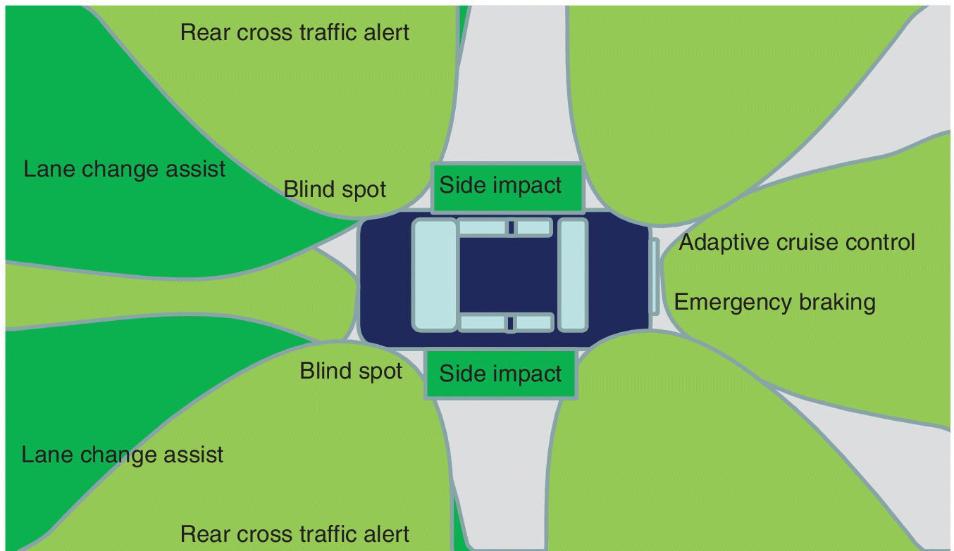
Figure 2.45 Illustration of typical ADAS system concepts in an automobile radar system.
Based on Autoliv, October 3, 2016 [87].
New applications in automotive add new requirements for eFlash. For example, in‐field programming updates by wireless communications and over‐the‐air (OTA) are expected. Low EMI noise in‐field programming is necessary for wireless communications that could be affected by various sources, including by operating noise generated by charge pump circuits in eFlash.
Many ADAS functions are expected to come before fully autonomous vehicles are common. These systems will require changes in the current architecture of the automobile control systems. Today cars typically have more than 50 electronic control units (ECU) that manage many aspects of the car’s performance and behavior [88]. The increasingly sophisticated controllers required for ADAS functions will require increased computing performance and connectivity as well as higher levels of safety and security. A potential future control system partitioning with ADAS, and eventually autonomous vehicles, is shown in Figure 2.46. At the lowest level of complexity will be the need for advanced environmental sensing, which will require ultrasonic, radar, lidar, and camera/vision systems. At the next level of complexity is recognition devices and classification systems. Calculations and decisions need to be made next, followed by either driver notification and/or automated system control response. The response systems in the automobile are at the next level and consist of: braking control systems, chassis control such as air bag activation, steering control such as in response to lane recognition, and powertrain control such as needed for active collision avoidance.
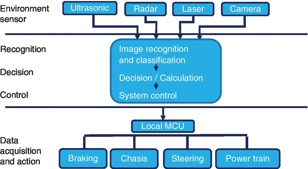
Figure 2.46 Possible future control system for ADAS and autonomous vehicles.
Based on J. Scobie and M. Stachew, EE Times, October 29, 2015 [88].
Initially these systems will be driver alert systems, followed by drive assist systems, followed at some time in the future with autonomous drive systems. Autonomous cars will be the ultimate feature.
2.9.2 Early Advanced Automotive Driver Assistance Systems
Early automotive control systems included such features as headlight control, electronic braking, and anti‐skid braking. Examples of such systems are shown in Figure 2.47.

Figure 2.47 Examples of early advanced driver assistance systems.
The early automotive control systems began to be introduced in the new millenium. An automotive meter control for instrument clusters for two wheeled vehicles was introduced by Renesas in October of 2012. This 16‐bit MCU was designed for two wheel and affordable four wheel vehicles for markets such as China, India, and Brazil [89]. They were intended to replace mechanical meters and gauges with electric meters where there is limited space for such meters. They included 256 KB of on‐chip Flash memory and LCD panel display capability. Odometer data could be saved on‐chip so an external EEPROM is eliminated. One to four channels of stepping motor controller/driver were included along with a sound generator.
Controllers for automotive body applications were also introduced early. In September of 2012, Renesas announced a 32‐bit MCU for automotive body applications [90]. The 40 nm chips had from 256 KB to 8 MB of on‐chip Flash memory. The eFlash chips were made in the MONOS charge trapping process. Power consumption for the MCU was 0.5 mA/MHz. An LIN interconnect network was on‐chip along with data encryption. The MCU core could operate at 80 MHz. It is targeted at air conditioner control or LED headlight control. The embedded Flash memory was intended for storing instructions and data. It could be reprogrammed up to 125 000 times per 64‐byte block, which permitted it to substitute for external EEPROM in many cases.
Electronic Braking was also an early driver assistance system. In November of 2012 Freescale announced a quad‐core MCU with two pairs of redundant cores for advanced electronic braking systems [91]. The chip used Continental’s fault recovery technology. The MCU contained 4.75 MB of Flash memory, 256 KB of SRAM, and Continental’s fail‐safe technology. The MCU was built in 55 nm technology.
Driver Assistance systems include electric power steering and anti‐skid control. An MCU chipset intended for use in these systems was introduced in October of 2012 by Texas Instruments. This chipset included a safety MCU with RISC core from ARM, which operated from 80 to 180 MHz using up to 1.23 MB of Flash memory [92]. It also included a multirail safety power management IC and a safety motor driver. These chips formed a safety motor control chipset intended for failure detection and mitigation. Target applications included advanced driver assistance systems, electric power steering, anti‐skid control, and other driver assistance systems.
Self‐parking autos were prototyped in 2013 with the Ford fully automated self‐parking car. Active Park Assist, which aided in parallel parking, was already available. Obstacle avoidance systems to actively detect objects in the road and warn drivers were being developed.
In October 21, 2014, TI announced a family of infotainment processors with added ADAS signal processing functionality [93]. The 1.4 GHz DSP had additional USB, video input, and PCLe interfaces. A second DSP core with 1.4 GHz of signal processing could be used to dynamically stitch multiple cameras into a single view. The added DSP performance included audio and speech processing and voice recognition. The processors included an RISC ARM core capable of supporting up to four 1080 displays and four 1080 video and camera inputs. High definition displays and megapixel cameras could be connected. Video, audio, and bidirectional I2C control signals could be carried concurrently over a single twisted pair cable. A power management IC was designed for seamless operation with the SoC.
2.9.3 More Recent Advanced Driver Assistance Systems (ADAS)
In January of 2016, NXP announced a single chip automotive radar sensor [94]. This 77 GHz radar transceiver provides precise data about the surrounding driving environment. Its small size permits it to be integrated invisibly anywhere in the car. Its power consumption is 40% lower than conventional radar ICs. Applications include: emergency braking, adaptive cruise control, blind spot monitoring, cross‐traffic alert, pedestrian protection systems, and automated parking. For a 360 degree view a number of radar sensors is required for robust high resolution. Future projects include a single chip automotive radar SoC, which might include the radar sensor.
Advanced driver assistance systems (ADASs) were targeted by GlobalFoundries in March of 2016 with plans for automotive ICs that used faster processors based on 22 nm fully depleted SOI (FD‐SOI), embedded MRAM, and 5G wireless communications circuits [95]. These ADAS systems in a car will require either radar or up to five cameras per car and the image processors must be fast enough to react instantaneously to things in the path of the car. GlobalFoundries expects that FD‐SOI technology will improve the linearity and insertion loss of RF circuits.
2.9.4 Automotive Navigation and Positioning
Satellite positioning for automotive navigation has been developed. In January of 2014, STMicroelectronics announced its Teseo III single chip positioning product family [96]. These chips are capable of receiving signals from multiple satellite navigation systems, including the Chinese BeiDou, the US GPS, European Galileo, Russia’s GLONASS, and Japan’s QZSS. The chip creates state‐of‐the‐art positioning accuracy and leverages STM’s sensor fusion as developed for automotive dead reckoning and assisted Global Navigation Satellite System (GNNS). By adding China’s BeiDou satellite tracking capabilities to the chip, the Teseo III increases accuracy and location precision in Asia as well as throughout the world. It will permit in‐car and marine navigation systems and telematics systems. It has good accuracy across urban, rural, and mountainous areas. The Teseo III is a single chip integrating RF, digital control, and Flash memory to enable simultaneous tracking of multiple satellites, even in areas with obstructions to satellite visibility. It has high indoor sensitivity. The Teseo III was expected to be available for sampling in Q12014.
Automated road access that includes RFID auto identification systems are already a reality. While the initial tags included a battery powered radio transmitter, the newer tags are adhesive stickers with a button sized microchip and a reflective antenna system that uses the windshield as part of the antenna. Removing the sticker after it is placed on the windshield separates the chip from the antenna, which invalidates the tag and helps prevent fraud. The glass windshield provides an amplification effect that is significantly reduced if the tag is not mounted on glass. While the Houston system uses an ATA communication protocol, other systems also use eGo and SeGo, which the tags also recognize along with ANSI INCITS 256‐2001 and ISO 10374. The scanner range is 31.5 feet at 915 MHz. The 915 MHz RFID tag includes a 2014‐bit read/write passive memory.
2.9.5 Under‐the‐Hood Applications
Under‐the‐hood automotive applications such as powertrain require nonvolatile memory. NOR Flash memory tends to be used for both code and data storage due to its high temperature reliability, 20 year data retention, and sub 30 ns random read access time. In September of 2013, Infineon and Technical University Munchen discussed a 65 nm eFlash macro for under‐the‐hood automotive applications [97]. A NOR Flash was used for the fast read access time. Read throughput was 5.7 GB/s and write throughput was 1.4 MB/s. The high read throughput rate used a multiple voltage domain multiplexer that permitted a low voltage read path. It also used a local ground referenced read circuit using a time domain source side sense amplifier. This permitted a low voltage sub‐50 mV swing read operation for high speed readout in the presence of more than 30 mV system noise. The triple poly‐embedded Flash memory cell allowed a sub‐5 μs low current write operation that enabled a high write throughput up to a junction temperature (T j) of 170 °C.
The 4 MB eFlash macro was made in 65 nm technology. The array was split into two memory banks of 2 MB each. To achieve the high read throughput, every memory bank had its own read path and used 280 sense amplifiers, which can be read in parallel. An analog block had charge pumps and reference circuits. A hierarchical bit‐line architecture was used to reduce RC delay. To reduce RC delay of the word‐line, the memory array of each bank is split into two tiles of 1 MB each with word‐line drivers between. The macro uses a hot source triple poly cell with dedicated select transistor and memory transistor, which permits fast write. Features for the memory macro are shown in Figure 2.48.
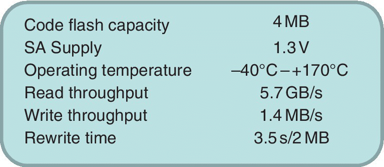
Figure 2.48 Features of memory macro for automotive powertrain applications.
Based on M. Jefremow et al. (Infineon, TU Munchen), ESSCIRC, pp. 193, September 2013 [97].
In April of 2014, Freescale, now NXP, announced its AEC‐Q100 qualified battery sensor with CAN protocol for mission critical automotive applications [98]. The part had a 16/32‐bit MCU and a CAN protocol module in a single package. The battery sensor integrated a 16/32‐bit S12Z MCU with 128 KB of Flash, 8 KB of SRAM, and 4 KB of EEPROM. The part measured key battery parameters and supported 12 V lead acid batteries along with 14 V stacked cell Li‐ion, high voltage junction boxes, and 24 V truck batteries. New features putting additional demand on batteries included: start–stop functionality, regenerative braking, and intelligent alternator control.
Flash MCUs with embedded Flash memory are essential in automotive applications for complicated real time controls for higher fuel efficiency, better safety, and increased connectivity. High density, fast random read access is needed from the eFlash. The requirements for eFlash in automotive are secured operations and data reliability, in particular reliable program/erase cycling at high temperature.
Automotive powertrain control applications require high performance CPU to help boost fuel efficiency, high speed network functionality to accommodate more sensors, and enhanced security to prevent unauthorized access and ensure safety. In April of 2016, Renesas introduced a 32‐bit MCU for automotive powertrain control [99]. The device was intended to meet increasing fuel efficiency goals along with engine control systems to optimize ignition and fuel injection timing along with boosting processing performance to accommodate increased levels of calculations. The MCU core had improved memory access latency at an operating frequency of 320 MHz at a junction temperature of 150 °C. It used the new Single Edge Nibble Transmission (SENT) digital communication standard for sensors and CAN FD5, which accommodates the increased volume of data from the increasing number of sensors, up to 50 currently. Security functionality was improved by the inclusion of an Intelligent Cryptographic unit hardware security module, which provided functions such as data encryption and cipher message authentication and random number generation.
2.9.6 MONOS Memory for Under‐the‐Hood Applications
Processors for automotive under‐the‐hood applications were discussed in April of 2015 by Renesas using embedded charge trapping memory of the metal oxide–nitride oxide semiconductor (MONOS) type, which can withstand the high temperatures associated with this application [100]. Over 100 Flash MCUs are used in the average car for various vehicle controls such as chassis, safety, body, and powertrain. The gas engine control is a high temperature application in the powertrain that requires intensive computation with a large program memory size at a junction temperature (T j) of 160 °C. Operating frequency for an automotive MCU by year is shown in Figure 2.49 along with frequency for the Renesas embedded MONOS Flash macro compared to an estimate of the operating frequency for floating gate Flash.
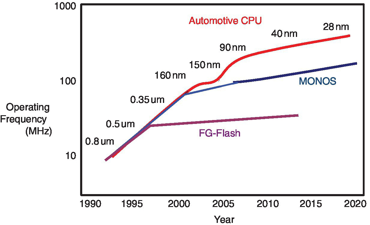
Figure 2.49 Operating frequency for an automotive MCU by year showing MONOS and FG Flash.
Based on T. Yamauchi (Renesas), VLSI‐TSA, April 2015 [100].
In February of 2016, Renesas discussed a 90 nm one transistor MONOS Flash memory that achieved over 100 million program/erase cycles at a high temperature of 175 °C with rewrite energy of 0.07 mJ/8 KB [101]. The 1 T‐MONOS Flash technology can be used with both CMOS and DRAM. It is expected that the Flash technology will enable Flash memory to be added to automotive analog devices, improving performance and reliability. In particular, the number of electronic control units (ECUs) being added per vehicle has been increasing and automotive control is becoming more complex. As a result, making the ECUs lighter and more power efficient is increasingly important.
The increase in number of motors in radiators, water pumps, and vehicle air conditioning systems has created a requirement for unification of mechanical and electrical elements so a technology that can add Flash memory to automotive analog and power controlling CPU devices is important. The high cycle endurance permits applications such as automatic calibration or status recording using high frequency sampling under actual field usage conditions. The current consumption during P/E operations is 98 μA. An idling program erase management unit function permits the Flash memory to control rewrites when the vehicle’s engine is stopped by an anti‐idling system. This makes it possible to stop the CPU and SRAM and reduce power consumption during idle by 99%. Trends for the code and data Flash for a 28 nm SG‐MONOS embedded Flash memory is shown in Figure 2.50. The memory cell size is 0.053 μm2 and operating temperature for the chip is specified at –40 to +170 °C junction temperature.
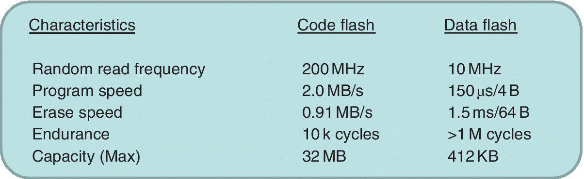
Figure 2.50 Code and data Flash characteristics in 28 nm SG‐MONOS embedded Flash memory.
Automotive temperature MRAM is also required in motorcycles. In May of 2015, Everspin announced that its automotive temperature MRAM meets the environmental requirements of the BMW 1000 RR Racing Bike [102]. A family of AEC‐Q100 fully qualified MRAM products for automotive applications has been introduced. The part is used in the BMW Motorrad Motorsport engine control unit, the RSM5, storing calibration data that controls the motorcycle during a race.
2.9.7 Automotive Infotainment
Devices intended for automotive infotainment require high speed interface, fast processor cores, and large amounts of embedded SRAM and NV Memory. In October of 2014, Atmel announced sampling of a family of MCUs with RISC core from ARM [103]. The devices ran up to 300 MHz and had 384 KB of SRAM as a system memory and up to 2 MB of on‐chip Flash memory. Ethernet AVB and Media LB peripherals made them suitable for automotive connectivity and audio applications. The devices also target applications including: the Internet of Things (IoT) and wearable devices. The devices include USB OTG and high speed USB PHY. The automotive series has Ethernet AVB support and Media LB for combination with Cortex‐M7 DSP for infotainment connectivity and audio applications.
Other examples of devices used for automotive infotainment include MCUs with video graphics. In March of 2016, Cypress Semiconductor discussed an expansion of its Automotive MCU family [104]. The MCU includes advanced graphics. The new MCU provides automotive manufacturers with a low cost platform for 2D and 3D graphics and enhanced functionality for dashboards, heads‐up displays and HVAC systems in compact vehicles. An earlier announcement of a 2D and 3D graphics MCU series for midsize cars was made in October of 2014 [105]. The graphics engine provides memory savings, increased safety features, and image capability without requiring external video RAM. This new family includes: an RISC processor core from ARM, 1 MB of embedded Flash, 1 MB of internal video RAM, enhanced secure hardware extension, and a HyperBus interface that permits connections with other HyperBus memories. These products are pin compatible with their predecessors, which provides flexibility and ease of upgrade with no changes in board layout. The chip also includes an advanced sound system and 16‐bit Audio‐DAC with multichannel mixer.
2.9.8 Secure Automotive
The 150–250 million connected cars expected on the roads by 2020 will be kept safe by chips with secure MCU. In February of 2016, STMicroelectronics announced a tamperproof MCU that was qualified for automotive applications to protect data privacy and system integrity [106]. Internet connectivity was expected to bring many services to vehicles such as software updates, service packs, location‐based information, social media, streaming entertainment content, and emergency support. The MCU was qualified to the automotive AEC‐Q100 standard. Additional security implemented by unalterable hardware permits use as an embedded Secure Element. Robust security in autonomous and driverless vehicles will enable car sharing. The part has 1280 KB of on‐chip user Flash to manage connections to multiple cellular networks.
2.9.9 Automotive Body Processors
Body controllers in automobiles include applications such as door modules, seat modules, and central body control. These body processors in automotive include airbag controllers such as a new automotive 55 nm 32‐bit MCU SoC designed for entry‐level vehicle safety‐critical applications [106]. This chip supports airbags and anti‐lock braking systems in cars and motorcycles as well as power steering and DC/DC converters for hybrid/electric vehicles. The part has clock speeds up to 80 MHz and is designed to resist soft error failures due to cosmic rays in vehicle control functions such as steering and braking.
Another example of an automotive body processor MCU was announced by NXP in April of 2016. It included high performance communication capabilities including: FlexRay, CAN, and LIN. It had up to 1.5 MB of embedded Flash memory for data storage [107]. Both the Flash memory and the SRAM included ECC. There was a 16 channel enhanced DMA and a memory management unit with a four‐entry translation look‐aside buffer. Operating frequency was 80 MHz.
For enhanced security, NXP also offered in July of 2016 a reliable 32‐bit MCU for automotive next generation automotive central body control [108]. The 55 nm chip had a hardware security module to protect against various hack attack scenarios. The previous generation chip was made in 90 nm technology. The device contained two 160 MHz cores along with an 80 MHz core for flexible power performance. There were 6 MB of embedded NVM Flash memory and 768 KB of eSRAM. New low power modes were supported. The hardware security module exceeded the requirements of the secure hardware extension (SHE) of the Hersteller Initiative Software standard. The devices were targeted at applications such as: door modules, seat modules, central body, vehicle body controllers, smart junction box, front module applications, and high end gateway applications.
2.10 Smart Electrical Grid and Digital Utility Smart Meters
2.10.1 Overview of the Smart Meter Market
Smart utility meters are configured for two‐way communication. They record the time of day that electricity is used, permitting different prices during different times. Power quality issues and other characteristics may also be recorded and transmitted.
Security issues with the utility infrastructure have been given serious consideration. Renesas forecasted in 2016 that the number of installations per year of smart meters with enhanced security features was expected to grow from 30 million in 2016 to 110 million in 2020 worldwide. Key issues have become security of power meter data and lowering meter prices [109]. The smart meter market by 2014 was estimated by Renesas at over 100 million smart meters in operation. This was in part driven by the requirement for home energy management systems [110].
2.10.2 Smart Meter Chips with Embedded Flash Memory
Smart meter chips use a range of MCU sizes running at speeds up to 80 MHz, active power in microamps to milliamps, and standby power in the microamp range. A summary of various smart meter chips is shown in Figure 2.51. The MCU and embedded nonvolatile memory contained in these chips are shown along with active current and standby current.
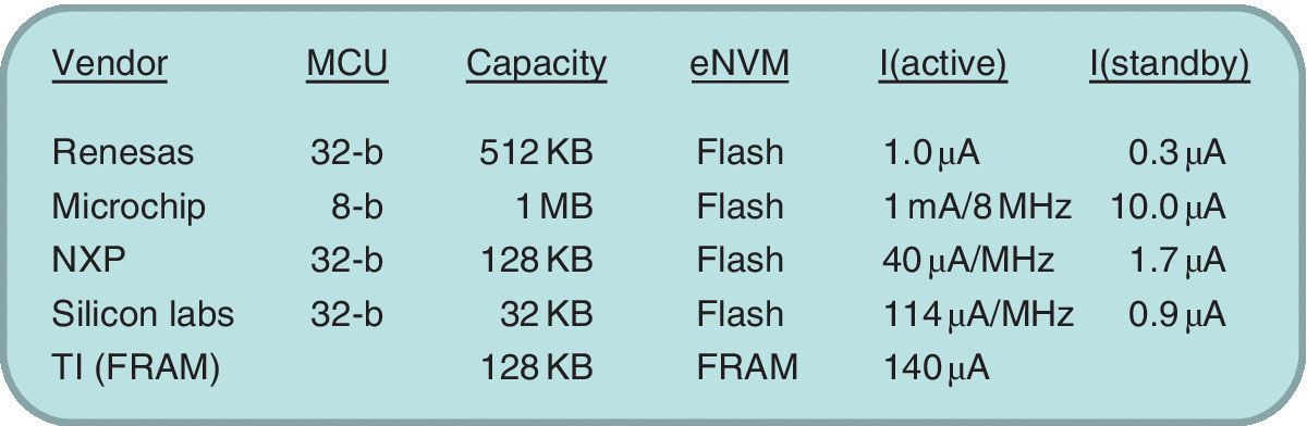
Figure 2.51 Smart meter chips from various vendors showing MCU and embedded nonvolatile memory along with chip active and standby current.
2.10.3 Smart Meter Chips with Large Embedded Flash Memory
Smart electricity meters log electric power parameters, such as power consumption, active power, reactive power, load conditions, voltage, and frequency distortion at regular intervals of milliseconds to seconds. Data are stored in the meter’s nonvolatile memory for periodic transmission to the system or the power grid.
A 32‐bit MCU intended for smart meters with advanced functionality was introduced by Renesas in September of 2012 [110]. The MCU includes 512 KB of embedded Flash memory, a 32‐bit CPU core, and a 24‐bit delta‐sigma A/D converter for high resolution measurement. The need for large Flash memory is driven by the need to accommodate larger programs. Power consumption in standby when the RTC is operating is 1.0 and 0.3 μA when the RTC is stopped.
A single chip powerline SoC for smart metering applications was announced by Atmel in October of 2012 [111]. The MCU has an RISC core from ARM, 2 MB of dual‐bank Flash memory, 160 KB of SRAM, and a fast PLC transceiver. The chip was compliant with the PRIME (Power Line Intelligent Metering Evolution) PLC specification. The SoC included an integrated low power amplifier that consumed 40% less power than comparable solutions. It includes an SPI. TSI and USARTS to support various communication interfaces are required in smart metering.
A photo is shown in Figure 2.52 of the electric meters in a home associated with a home solar generating facility and a community electric utility. The meter on the left runs forward and measures electricity generated by the rooftop solar array. The meter on the right is connected to the community electric utility and indicates the electrical usage from the utility net of that generated by the solar panels. It runs both forward and backward depending on the net direction of the electricity being generated.

Figure 2.52 Illustration of electric meters connected between a home solar generating facility and an electric utility. The meter on the left measures electricity generated by the solar array and the one on the right shows net usage of the community and solar facilities.
Photo by Dr. J.H. Ericksen, with permission.
An energy efficient 32‐bit sub‐GHz wireless MCU was announced in October of 2012 by Freescale (now NXP). The MCU, which used a 32‐bit low power RISC core from ARM, ran up to 48 MHz with 128 KB of Flash and 16 KB of SRAM [112]. Active power consumption was as low as 40 μA/MHz. Standby current was 1.7 μA/device with a 4.3 μs wake‐up. The device was suited for wirelessly networked smart energy applications. The chip has a 600 Kbps radio with complex modulation schemes and multiple frequencies supporting US and International protocols. It can support neighborhood area networks connecting smart meters to a common data collection point or networks of street lamps or sensors. This chip can run low level wireless protocol layers while delegating upper network protocol layers to an external host processor.
Development of a chip intended for smart electricity meters and data concentrators was announced in January of 2013 by the Atmel and Wasion Group [113]. The chip was to be based on several Atmel chips and an MCU with an RISC core from ARM; 2 Mb of Flash memory was to be included on the chip.
An MCU, targeted at the smart meter application, offering up to 8Mbits of embedded Flash memory, was introduced in February of 2013 by Microchip Technology [114]. The embedded memory was made in a split‐gate, NOR embedded Flash technology with a thick oxide tunneling injector. The parts have an extended operating voltage range from 2.3 to 3.6 V. The memory is partitioned into uniform 4 KB sectors and 32 and 64 KB blocks, offering seamless partitioning for program and data code in the same memory block. Sector and block erase is as fast as 18 ms and the entire chip can be erased in 35 ms. The word program time is 7 μs. Endurance is 105 cycles and more than 100 year data retention. Active read current is 10 mA typical at 80 MHz and standby current is 10 μA typical.
As the rate of smart meter deployments continue to rise in Europe and Asia, the demand for smarter and better integrated meters continues. In October of 2014 [115], Atmel announced a dual core secure MCU for smart metering applications. Each of the dual cores has 2 MB of cache‐enabled dual bank Flash, which are pin‐to‐pin compatible with existing 512 KB and 1 MB devices already in the field. The parts are built on a dual‐core 32‐bit RISC architecture. The devices also include: advanced security features, a low power real time clock, LCD driver, and several serial interfaces.
A low power MCU with up to 128 KB of ferroelectric nonvolatile memory replacing the Flash for low power data storage was discussed in September of 2014 by Texas Instruments [116]. The FeRAM MCU included an extended scan interface that autonomously manages and monitors four external sensors. It was targeted for flow meters for water, gas, and heat. There was a 140 μA differential input ADC. Other peripherals included: a 320 segment LCD controller, a 256‐bit hardware encryption accelerator for secure data transmission, and an intellectual property encapsulation module to protect code. The part had a fast write speed and low peak currents.
In March of 2015, Silicon Labs introduced an ultralow power 32‐bit MCU with a low power RISC core from ARM for Smart Metering applications [117]. The device had a short wake‐up time from energy saving modes and a selection of peripherals. Features included a 24 MHz RISC MCU from ARM, up to 32kB of Flash, and a 4 KB RAM memory. A single 1.98–3.8 V power supply was included and the devices worked over the industrial temperature range from –40 to 85 °C. Flexible energy management included: 20 nA shutoff mode, 0.5 μA stop mode, with power‐on reset, brown‐out detection, RAM and CPU retention, 0.9 μA deep sleep mode, 48 μA/MHz sleep mode, and 114 μA/MHz run mode with code executed from Flash.
Smart electricity meters using ferroelectric RAM memory were discussed in November of 2015 by Cypress Semiconductor [20]. Smart meters have conventionally used serial EEPROM to record data such as power consumption, active power load conditions, voltage, and frequency distortion. A 1 MHz 1 MB I2C EEPROM with 256 B page takes 28 ms to back up 1 KB of data, while an FeRAM takes 8 ms to write 1 KB of data into the FeRAM. FeRAMs consume about one‐third of the active current of EEPROM while the standby current is nearly the same.
In November of 2015, Microchip announced an addition to its low power MCU portfolio which includes up to 1 MB of dual partition Flash memory with ECC and 32 KB of RAM [118]. This permits programming of one partition while executing application code from the other. The chip is targeted at industrial, computer, medical, and portable applications that require a long battery life and data transfer and storage without needing external memory such as electrical meters.
An MCU with enhanced security function and improved arithmetic operations was announced in August of 2016 by Renesas for the smart power meter market [109]. The part retained the measurement accuracy and the low power consumption of the previous chip while adding the extra security functions. On‐chip memory capacity ranged from 64 KB for low end single phase meters to 128 KB for high end single phase meters and up to 256 KB for three phase meters. Security was enhanced by requiring authentication and encryption/decryption functions. An AES hardware engine was integrated for this purpose, which boosted speed by 20 times or more compared with en/decryption using software processing. The on‐chip PLL boosts the maximum operating frequency from 24 to 32 MHz. The 32‐bit multiply and accumulate unit reduces the load imposed by software power calculation by using a 24‐bit Delta Sigma A/D converter, which results in an approximate 30% increase in arithmetic capacity. The chips can support distribution line message specification (DLMS) standard communications while processing electric power measurement. This standard was enacted for smart meters. Program code is stored in 256 KB of on‐chip ROM for both electric power measurement and DLMS processing, leading to 30% reduced power consumption compared to a two chip implementation. System cost is also reduced. Standby mode current consumption is typically 0.7 μA during operation. An independent power supply and power monitoring with battery backup enabled the CPU to continue operating even in a power outage.
2.11 Consumer Home Systems and Networks
Home IoT control systems potentially include: environmental control, access control, vision systems, light control, comfort control (auto adjusting beds and chairs), information control, entertainment control, food and water control, safety alerts (tornado, fire, flood), animal access, and care and child monitoring and care. Initially remote control of these systems cannot be provided to the owner. Eventually such systems will be automated and robotic. Figure 2.53 indicates the home network of connected systems.
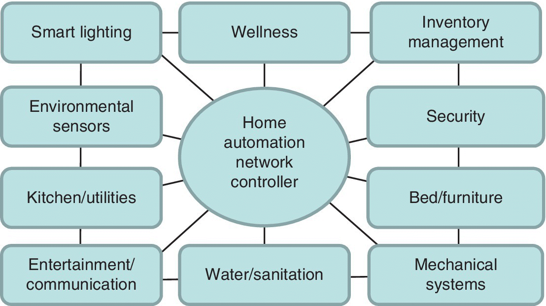
Figure 2.53 Home network of connected systems with central home automation.
2.11.1 Remote Controls
In October of 2012, TI announced its low cost, value 2.4 GHz RF line of SoC for remote control applications, which supported 2.4 GHz frequency bands [119]. The SoCs integrate an MCU, 32KB of Flash and 2KB of RAM on chip. The data rate is 2 Mbps with <1 μA sleep current with the sleep timer running.
In January of 2013, Energy Micro announced an MCU expected to be used in the VELUX touch screen remote control, where it keeps the handheld control asleep with a 1.2 μA low energy capacitive tough sensor interface [120]. The 32‐bit MCU has 1 MB of Flash memory with the added option of embedded USB connectivity. CPU speed is up to 48 MHz. The MCU includes autonomous low energy peripherals such as AES encryption, a pulse counter, low energy UART, and others.
2.11.2 Environmental Sensors
Sensors for the internal home environment are useful in home networks and may use energy harvesting to avoid battery maintenance. In June of 2016, Cypress Semiconductor discussed a tiny light powered sensor beacon that wirelessly transmitted data it had sensed in the surrounding environment [121]. This sensor can sense temperature and humidity around its location and transmit the data using Bluetooth Low Energy. The beacon is 25 mm in diameter and needs no battery maintenance. It is powered by in‐doors ambient light as low as 100 lux, which is less light than a typical warehouse aisle receives. The beacon can be connected to a host PC using a USB interface for data and debugging. It comes with an app for IOS, Android, and PCs, which enables transmitting data as a graph or data. Its startup power is 1.2 μW and current consumption is as low as 280 nA.
2.11.3 Home Network Systems
Smart lighting and home automation require wireless sensor networks. In November of 2012, NXP announced a family of wireless MCU for ZigBee, JenNet, and other IEEE 802.15.4 applications [122]. The chip integrated a 2.45 GHz radio, analog peripherals with MCU on a chip. It included up to 256 KB of eFlash, 4 KB of EEPROM, and 32 KB of SRAM to support network stacks. It has an in‐packet antenna diversity that chooses the best antenna on every packet received. Target application is the home networks of connected systems. This includes such things as smart lighting, home automation, and wireless sensor networks as well as other home essentials, as was shown in Figure 2.53.
2.12 Motor Control Chips with Embedded Memory
Flash MCU for motor control falls into two categories, small motors with 8‐bit MCU and up to 64 KB of embedded Flash and more complex motors with 32‐bit MCU and up to 1 MB of eFlash.
2.12.1 Small System Motor Control Using Embedded Memory
Small system motor control is required in household appliances and home healthcare as well as for fans, tools, battery charges, and many other consumer home appliances that can be connected.
An MCU family targeted at low power consumer, household appliance, and home healthcare was announced by Renesas in September of 2014 [123]. A motor control kit was being offered to support Internet and cloud connectivity. The kit supports three‐phase and brushless DC motors. The MCU has a 140 μA/MHz RL78 core, 5 V power supply, and up to 256 KB of Flash memory.
An 8‐bit MCU portfolio for IoT with one version intended for small system motor control applications such as fans and tools, power supplies, battery chargers, and sensor controllers was introduced in February of 2016 by Silicon Labs [124]. There are three versions, which include low power capacitive touch control and USB connectivity. Core speeds are up to 50 MHz and there are 2–16 KB Flash sizes. Peripherals include a 12‐bit analog‐to‐digital converter (ADC).
In March of 2016, Toshiba announced an RISC MCU in 65 nm logic with embedded Flash memory [125]. The MCU included high performance analog and a range of functions for motor control. Flash memory ranges from 32 to 128 KB for code and 8 to 18 KB for data. Other features integrated included a high precision 12‐bit ADC and an 8‐bit DAC. The maximum operating frequency is 40 MHz. Peripheral circuits included on the chip include: UART, I2C, TSPI, and timers.
2.12.2 Motor Control for Multiple Motors Using Embedded MONOS Memory
In November of 2012, Renesas announced an MCU intended to provide inverter control for up to three 3‐phase motors simultaneously [126]. A 32‐bit RX CPU core operated at 100 MHz without a wait state using embedded MONOS Flash memory. The memory size has been increased up to 512 KB of Flash and up to 48 KB of SRAM. An additional independent 32Kb of data Flash was included for background operations to enable data to be written while a program is executing. Performance was 1.65 DMIPS/MHz at any CPU frequency without limitation from the memory.
In March of 2016, Renesas announced a 32‐bit MCU group that enabled simultaneous inverter control of multiple motors with a single chip and doubled the performance of the MCU group [127]. These MCU were also targeted household appliances as well as industrial motor applications. On‐chip Flash capacity ranged up from 128 KB. These MCU were ideally suited for permanent magnet AC (PMAC) motor control. They had 160 DMIPS with dedicated analog functions to increase the arithmetic operation and expand motor control peripheral functions. The MCU had on‐chip FPU functionality for faster code execution. The TXv2 CPU core had a five‐stage pipeline, a floating point unit, and DSP functions. It ran at 80 MHz. The FPU functionality provided faster implementation of calculation of intensive algorithms with a wide dynamic range.
2.12.3 Motor Control with Embedded NV FeRAM
Low cost industrial and metering applications were targeted by TI in May of 2015 for their microcontroller with 64 KB of embedded NV FeRAM [128]. A new technology permitted context save and restore. The technology featured instant wake‐up with intelligent system state restoration after an unexpected power loss. The chip also included integrated smart analog and digital peripherals to reduce system cost, power, and size including: a low power segment LCD controller, a 12‐bit differential ADC with internal window comparator, a 256‐bit AES accelerator, and LCD. The 16‐bit MCU could be used for datalogging for wireless motor condition monitoring. The chip can be used with TI’s energy harvesting IC and wireless MCU to operate from a coin cell battery for decades. The system can be used to monitor and analyze motor vibration frequencies to predict and schedule maintenance in automated environments.
2.13 Smart Chip Cards in Advanced Applications
For advanced inventory control applications, in March of 2014, EMM discussed a universal identity card and an encrypted tamperproof digital certificate [129]. The security measures of the device used public stream cipher technology to guard the memory data integrity. 2 K‐bits of data memory were included in the device. Each device had a unique embedded EEPROM 64‐bit identifier and optional 32‐byte ECC‐based digital certificate. An NFC enabled smartphone can read out these pieces of information and confirm the authenticity of a good by connecting to a cloud server that manages the collected data.
An advanced secure IC Flash MCU family for secure EMV (Eurocard/Mastercard/Visa) chip payment cards was announced in May of 2014 by ST Microelectronics [130]. This was intended as a family of secure payment card chips. Chip cards that embed an EMV‐compliant secure chip can store and process data securely and are difficult to replicate. This family of chips was based on a secure IC in 90 nm technology. The cards used a 32‐bit secure RISC core from ARM along with a contactless interface. The cards had up to 38 KB of installable EEPROM.
For payment applications, a third generation of secure MCU was announced in November of 2015 by STMicroelectronics. These chips had 2 MB of 40 nm eFlash program memory, fast clock speed, and a fast embedded cryptographic accelerator based on a 32‐bit secure RISC core from ARM [131]. The hardware architecture provided multiple strong fault protection mechanisms for CPU, and memory and buses for secure software and systems. It met the need for secure applications in areas such as payment applications and wearable consumer devices, machine‐to‐machine communications in “Industry 4.0” factory automation, and automotive in‐car communications. The peripheral had a secure Data Encryption Standard (EDES) algorithm and the NESCRYPT cryptoprocessor supported the public key algorithm. The 2 MB eFlash memory permitted the device to host a variety of applications.
For home banking and USB readers, in February of 2016, NXP announced its PN7462 family of NFC controllers that combine a low power 20 MHz ARM Cortex M0 MCU core with USB and NFC [132]. This chip had advanced power management as well as a 160 KB Flash and 4 KB EEPROM. Interfaces were: UART and ISO/IEC7816.
2.14 Analysis of Big Data Server Memory Hierarchy for Storing IoT
Items that can accessed and tracked through the Internet range from automobiles, to home security systems, to retail inventory, to factory items in process, to individual pieces of fruit in the grocery store. The current Internet protocol allows a massive number of items to be uniquely identified. Internet protocol version 6 (IPv6) uses 128 bit addresses that allow over 1038 separate items to be identified and located across networks. These networks require powerful processors to transfer and process huge amounts of information and large memories that can store this information.
Real time tracking can record both the flow of goods as they move through various systems over time, the changes in these goods, and also changes in measurements taken by stationary sensors over time. Flow could involve people flowing through cities, patients moving through hospital routines, goods moving through factories, energy flowing through networks, or automobiles moving along highways. Changes recorded could involve everything from processing of items being created in factories to food that is stored in refrigerators being consumed and aging.
This massive amount of “Big Data” is stored in large networks of servers, which are referred to as “the Cloud”. The Internet of Things uses mainstream memories in large server farms where individual IDs for millions of sensors are stored and can be accessed from, for example, a cell phone. This involves sorting rapidly though large amounts of data using sophisticated search engines. A sophisticated memory hierarchy is required for rapid access of these large server farms. This is shown in Figure 2.54, which illustrates a cache hierarchy for servers that could be used in large server farms along with a potential search engine to be used for Big Data analysis. The circuits shown here were presented at the ISSCC Conference in February of 2016 and are intended to illustrate the state‐of‐the‐art in these classes of circuits at a single point in time.
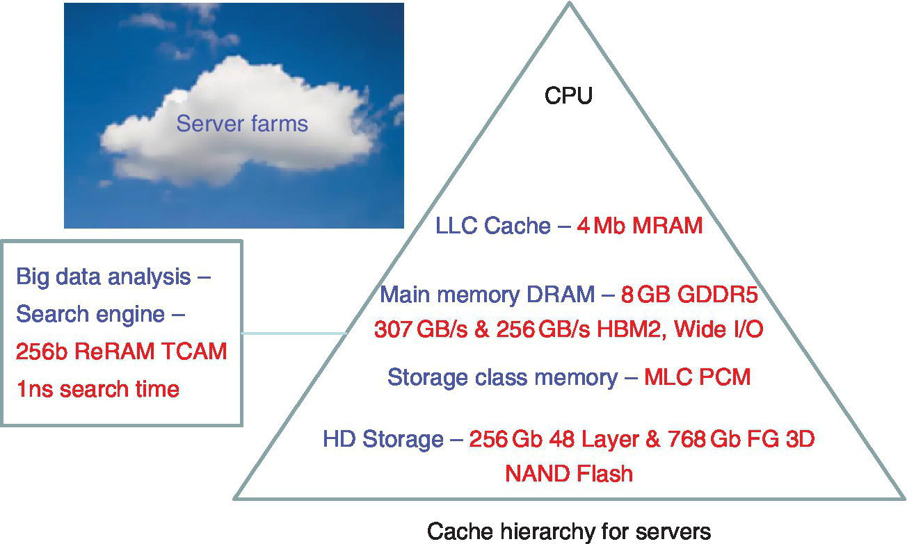
Figure 2.54 Memories for tomorrow’s Cloud applications (collected from devices shown at the 2016 ISSCC).
An example of a “Big Data” analysis search engine that operates on the data in the server farm could be a Ternary Content Addressable Memory (TCAM). SRAM‐based TCAMs have been used in the past as search engines. A 256‐bit 2.5 Transistor 1 Resistor (2.5T1R) Resistive RAM (RRAM) TCAM search engine was designed for this purpose in 2016 by NTHU, TSMC, and NCTU [133]. The RRAM was used to increase chip capacity by reducing cell area over that of an SRAM. An RRAM can also reduce search energy and standby power over that of SRAM‐based TCAM in applications with long idle times and frequent‐search‐few‐write operations. This RRAM cell was made in a 65 nm fully CMOS compatible process at the TSMC foundry.
Embedded SRAM has traditionally been used for cache in large servers due to its high speed, ranging from 1 ns to 10 ns in the various levels of cache. As advanced CMOS technologies have gone to lower power supply voltages, embedded SRAMs have increasingly suffered from subthreshold leakage, which affects their energy consumption and reliability. A magnetic RAM (MRAM) has sufficient capacity and switches fast enough to be used as a last level cache (LLC). It is nonvolatile so it consumes no power in standby, which enables it to reduce the total energy compared with a conventional SRAM last level cache (LLC). A 4 Mb magnetic RAM (MRAM) cache designed for use as an LLC was discussed by Toshiba. It was configured as a four‐way SET Associative cache with a 362 K‐bit SRAM TAG [134]. The MRAM cache reduced total energy by 93% compared with a conventional SRAM LLC with a read‐modify‐write function. Standby energy was reduced by 77%.
Below the cache in the memory hierarchy is the main memory, which consists primarily of high density banks of DRAM. The operation of the DRAM at about 100 ns is slower than the SRAM cache but much faster than the mass storage below it, which consists of high density nonvolatile Flash memory.
Capacity of a DRAM chip can be as high as 8 GB or 64 Gbits. A fast high bandwidth memory (HBM) wide I/O DRAM was shown by Samsung [135] with 8 GB capacity. It used the GDDR5 high bandwidth memory (HBM) interface. The HBM had 160 GB/s of memory bandwidth but uses up to 70% less energy per bit than other technologies.
A new category of memory being explored is the storage class memory, which is envisioned as bridging the speed gap between the main memory and the Flash memory mass storage. A concept of a classical memory hierarchy that includes storage class memory is shown in the diagram in Figure 2.55.

Figure 2.55 Memory hierarchy including the storage class memory.
The access time latency goes up, that is the access time becomes slower, as we go down the memory hierarchy. The memory capacity, however, goes up. A processor can run at 1 ns, SRAM tends to run at 10 ns, and main memory DRAM at 100 ns. Mass storage speeds are around 100 μs with archival mass storage slower than a millisecond. The storage class memory is envisioned as filling the gap from 100 ns to 100 μs. A multilevel cell phase change memory (PCM) was shown by Macronix, NTHU, NCTU, and IBM and is an example of a potential storage class memory with access latency in the 1 to 10 μs range [136].
Hard drive storage is currently provided by vertically stacked chips up to 256Gb with 48 layers of 3D Flash memory chips [137] and 768Gb 3b/cell floating gate 3D NAND Flash [138] or a 128Gb 2b/cell NAND Flash memory in 14 nm planar NAND Flash technology [139].
References
- 1 Kono, T. et al. (2014) 40‐nm embedded split‐gate MONOS (SG‐MONOS) Flash Macros for automotive with 160‐MHz random access for code and endurance over 10 M cycles for data at the junction temperature of 170 °C (Renesas). IEEE Journal of Solid‐State Circuits, 49 (1), 154, January 2014.
- 2 Milani, L., Torricelli, F. and Kovacs‐Vajna, Z. (2015) Single‐poly‐EEPROM cell in standard CMOS process for medium‐density applications (Univ. Brescia). IEEE Trans. on Elec. Dev., 62 (10), October 2015.
- 3 Kang, S.H. (2014) Embedded STT‐MRAM for energy‐efficient and cost‐effective mobile systems (Qualcomm Technologies), VLSI Technology Symposium, June 2014.
- 4 Adesto Technologies and TPSCo Announce CBRAM Manufacturing Agreement, Adesto Press Release, February 25, 2016.
- 5 Joosting, J.P. (2015) Shanghai Huali Microelectronics looks to specialty technology to target IoT growth. EE Times, January 1, 2015.
- 6 Lee, Y.K. et al. (2014) A 45‐nm logic compatible 4 Mb‐split‐gate embedded Flash with 1M‐cycling endurance (Samsung), IMW, May 2014.
- 7 Yamauchi, T. (2015) Prospect of embedded non‐volatile memory in the Smart Society (Renesas), VLSI‐TSA, April 27, 2015.
- 8 Jew, T. (2015) Embedded microcontroller memories (Freescale), IMW, May 2015.
- 9 STM32F0 entry‐level ARM Cortex MCUs (2016) STMicroelectronics website, August 2016.
- 10 Texas Instruments introduces 32‐bit MSP432 Microcontrollers (MCUs): ultra‐low power at its best, performance at its core, TI Press Release, March 24, 2015.
- 11 Jayamumar, H., Raha, A. and Rahunathan, V. (2014) QUICKRECALL: A low overhead HW/SW approach for enabling computations across power cycles in transiently powered computers (Purdue University), Conference on VLSI Design, January 5, 2014.
- 12 Kaneko, Y., Nichitani, Y., Ueda, M. and Omote, A. (2014) Battery‐less impact‐logging device consisting of a vibration energy scavenger and ferroelectric memory (Panasonic), Device Research Conference, pp. 65, June 22, 2014.
- 13 Ishii, T. et al. (2015) 0.6 V operation, 26% smaller voltage ripple, 9% energy efficient boost converter with adaptively optimized comparator bias‐current for ReRAM Program in low power IoT embedded applications (Chuo University), IEEE A‐SSCC, November 2015.
- 14 Cypress introduces the world’s lowest‐power energy harvesting power management ICs for battery‐free wireless sensor nodes, Cypress Press Release, August 19, 2015.
- 15 BQ25570 ultra low power harvester power management IC with boost charger and nanopower buck converter, TI Data Sheet, 8/2016.
- 16 STM32 32‐bit ARM Cortex MCUs, STMicroelectronics website, September 2016.
- 17 STMicroelectronics launches new STM32 ultra‐low‐power microcontrollers for consumer, health, and industrial applications, ST Micro Press Release, February 11, 2014.
- 18 Cypress introduces the industry’s most energy‐efficient ARM Cortex‐M0+ MCUs for ultra‐low‐power Internet of Things applications, Cypress Press Release, December 2, 2015.
- 19 Panasonic starts world’s first mass production of ReRAM mounted microcomputers, Panasonic Press Release, July 30, 2013.
- 20 Panasonic and UMC Partner for 40 nm ReRAM process platform, Panasonic Press Release, February 2, 2017.
- 21 Baumann, A. et al. (2013) A MCU platform with embedded FeRAM achieving 350 nA current consumption in real‐time clock mode with full state retention and 6.5 µs system wakeup time (Texas Instruments), VLSI Circuits Symposium, June 12, 2013.
- 22 TI introduces the world’s first microcontroller with a configurable low‐leakage transimpedance amplifier, TI Press Release, March 22, 2016.
- 23 Qazi, M., Amerasekera, A. and Chandrakasan, A.P. (2013) A 3.4 pJ FeRAM‐enabled D flip‐flop in 0.13 µm CMOS for nonvolatile processing in digital systems (MIT, TI), ISSCC, February 2013.
- 24 Khanna, S. et al. (2013) Zero leakage microcontroller with 384 ns wakeup time using FeRAM mini‐array architecture (TI, TSMC), A‐SSCC, pp. 21, November 11, 2013.
- 25 Khanna, S. et al. (2014) An FeRAM‐based nonvolatile logic MCU SoC exhibiting 100% digital state retention at VDD = 0 V achieving zero leakage with <400 ns wakeup time for ULP applications (Texas Instruments), IEEE Journal of Solid‐State Circuits, 49 (1), 95, January 2014.
- 26 Koike, H., Sakimura, N. et al. (2013) A power‐gated MPU with 3‐microsecond entry/exit delay using MTJ‐based nonvolatile flip‐flop (Tohoku University, NEC), A‐SSCC, November 11, 2013.
- 27 Sakimura, N. et al. (2014) A 90 m 20 MHz fully nonvolatile microcontroller for standby – power‐critical applications (NEC, Tohoku University), IEEE ISSCC, February 2014.
- 28 Qazi, M., Amerasekera, A. and Chandrakasan, A.P. (2014) A 3.4‐pJ FeRAM‐enabled D flip‐flop in 0.13‐µm CMOS for nonvolatile processing in digital systems (Cypress, MIT, TI). IEEE JSSC, 49 (1), 201, January 2014.
- 29 Kazi, I. et al. (2014) Energy/reliability trade‐offs in low‐voltage ReRAM‐based non‐volatile flip‐flop design (EPFL). IEEE Trans. on Circuits and Systems. –I: Reg.Papers, 61 (11), November 2014.
- 30 Vianello, E. et al. (2014) Resistive memories for ultra‐low‐power embedded computing design (CEA LETI), IEDM, December 2014.
- 31 Lee, A. (2015) RRAM‐based 7T1R nonvolatile SRAM with 2× reduction in store energy and 94× reduction in restore energy for frequent‐off instant‐on applications (NTHU, NDL, National Chung Hsin University, EOL ITRI), Symposium on VLSI Technology, June 2015.
- 32 Liu, Y. et al. (2016) A 65 nm ReRAM‐enabled nonvolatile processor with 6× reduction in restore time and 4× higher clock frequency using adaptive data retention and self‐write‐termination nonvolatile logic (Tsinghua University, National Tsing Hua University, University of California, Los Angeles), ISSCC, February 2016.
- 33 Levisse, A. et al. (2014) OxRAM‐based pulsed latch for non‐volatile flip‐flop in 28 nm FDSOI (University of Grenoble Alpes), IEEE SOI‐3D‐Subthreshold Microelectronics Technology, October 6, 2014.
- 34 Radio‐frequency identification, Wikipedia, the free encyclopedia, 1 August 2017.
- 35 Prophet, G. (2015) Panasonic’s NFC + FeRAM technology and platform, now in distribution, www.rs‐online.com, February 20, 2015.
- 36 Worlds first fully integrated NFC & EPC Gen2V2 dual‐frequency RFID solution from EMMicroelectronic, Press Release, April 14, 2015.
- 37 NXP’ NTAG I2C plus extends the family of connected NFC tags to specifically address the smart home market, NXP Press Release, February 23, 2016.
- 38 Swedberg, C. (2014) Macy’s expands RFID and Beacon Deployments. RFID Journal, September 16, 2014.
- 39 EM Microelectronic now shipping FCC/CE/IC certified Bluetooth® SMART beacons, EM Microelectronic Press Release, December 9, 2014.
- 40 About nRF51822, Nordic Semiconductor Press Release, June 12, 2012.
- 41 Silicon Labs simplifies Bluetooth smart design with fully integrated blue gecko module, Silicon Labs Press Release, August 17, 2015.
- 42 Toshiba’s new ICs for Bluetooth® smart devices feature built‐in Flash ROM, Toshiba Press Release, November 17, 2015.
- 43 Silicon Labs advances Bluetooth smart connectivity with energy‐friendly SoC and S software solution, Silicon Labs Press Release, February 23, 2016.
- 44 Smallest Microcontroller in STMicroelectronics’ STM32 F4 Series enters production, with easy‐access development support, STMicroelectronics, December 3, 2015.
- 45 TI’s new sub‐1 GHz solution spans 20 km on a coin cell, TI Press Release, November 18, 2015.
- 46 Silicon Labs simplifies Wi‐Fi connectivity with plug‐and‐play module solution, Silicon Labs Press Release, February 2016.
- 47 Silicon Labs simplifies IoT connectivity with multiprotocol wireless Gecko SoCs, Silicon Labs Press Release, February 2016.
- 48 Silicon Labs introduces world’s most energy friendly USB microcontrollers, Silicon Labs Press Release, May 13, 2015.
- 49 Silicon Labs rolls out next‐generation 8‐bit microcontrollers for the IoT Age, Silicon Labs Press Release, February 23, 2015.
- 50 Atmel introduces world’s most innovative 2‐pin, self‐powered Serial EEPROM targeting the IoT, battery, consumable and cable identification markets, Atmel Press Release, August 10, 2015.
- 51 Zigbee, Wikipedia, the free encyclopedia, 26 July 2017.
- 52 Frenzel, L. (2012) What’s the difference between Bluetooth low energy and ANT? Electronics Design, November 29, 2012.
- 53 Izumi, S. et al. (2014) A wearable healthcare system with a 13.7 μA noise tolerant ECG processor (Kobe University, Rohm, Omron). IEEE Trans. on Biomedical Circuits and Systems, November 2014.
- 54 Fujitsu releases new 1 Mbit and 2 Mbit FeRAM products, Fujitsu America Press Release, March 21, 2013.
- 55 Gilbert, N., Zhang, Y., Dinh, J. et al. (2013) A 0.6 V 8pj/write non‐volatile CBRAM macro embedded in a body sensor node for ultra low energy applications (Adesto, University of Virginia), VLSI Circuits Symposium, June 2013.
- 56 Umeki, Y., Yanagida, K., Tsunoda, K. and Sugii, T. (2013) A 0.38‐V operating STT‐MRAM with process variation tolerant sense amplifier (Kobe University, LEAP), A‐SSCC, pp. 249, November 11, 2013.
- 57 Yamashita, K. et al. (2013) A 38 μA wearable biosignal monitoring system with near field communication (Kobe University, Omron Healthcare), NEWCAS, June 2013.
- 58 Izumi, S. et al. (2013) A 14 μA ECG processor with robust heart rate monitor for a wearable healthcare system (Kobe University, Rohm Co., Omron, Omron Healthcare, JST CREST), ISCDG, September 13, 2013.
- 59 Izumi, S. et al. (2014) A wearable healthcare system with a 13.7 μA noise tolerant ECG processor (Kobe University, Rohm, Omron). IEEE Trans. on Biomedical Circuits and Systems, November 2014.
- 60 Izumi, S. et al. (2014) Normally‐off technologies for healthcare appliances (Kobe, Rohm), ASP‐DAC, pp. 17, January 20, 2014.
- 61 NXP and GlobalFoundries announce production of 40 nm embedded non‐volatile memory technology, NXP and GlobalFoundries Press Release, March 24, 2015.
- 62 TSMC launches ultra‐low power technology platform for IoT and wearable device applications, TSMC Press Release, September 29, 2014.
- 63 Toshiba develops two new process technologies for microcontrollers and wireless communication ICs, Toshiba Press Release, July 6, 2015.
- 64 NXP ships LPC11U30 USB microcontrollers with 128 KB Flash, NXP Press Release, June 25, 2012.
- 65 Texas Instruments unveils the Stellaris® LaunchPad – a fully‐functional, flexible and low‐price kit for ARM® Cortex™ – M4 developers, TI Press Release, September 25, 2012.
- 66 Pikhay, E. et al. (2012) Radiation sensor based on a floating gate device (TowerJazz), IEEE Israel, p. 1, November 14, 2012.
- 67 Microchip expands SPI Flash memory portfolio with three new low‐power devices, Microchip Press Release, February 4, 2013.
- 68 STMicroelectronics launches new STM32 ultra‐low‐power microcontrollers for consumer, health, and industrial applications, ST Micro Press Release, February 11, 2014.
- 69 Develop the next generation of wearables with TI’s ultimate NFC wearable design challenge, TI Press Release, June 9, 2015.
- 70 Atmel Smart ARM Cortex M7‐based MCU and AVR powers TomTom Spark GPS fitness watches, Atmel Press Release, November 5, 2015.
- 71 Toshiba expands line‐up of ApP Lite(TM) processor family for IoT solutions, Toshiba Press Release, September 4, 2015.
- 72 Atmel launches ultra‐low‐power connected platform for cost‐optimized IoT and wearable applications at CES 2016, Atmel Press Release, January 5, 2016.
- 73 Silicon Labs rolls out next‐generation 8‐bit microcontrollers for the IoT Age, Silicon Labs Press Release, February 23, 2015.
- 74 Zenta from Vinaya uses Nordic semiconductors recently‐introduced nRF52832 SoC to wirelessly monitor and record a range of key biological and environmental data, Nordic Semiconductor Press Release, August 10, 2016.
- 75 Nordic nRF52 Series redefined single‐chip Bluetooth Smart by marrying barrier‐breaking performance and power efficiency with on‐chip NFC for touch‐to‐pair, Nordic Semiconductor Press Release, June 16, 2015.
- 76 Panasonic to manufacture embedded ReRAM microcontrollers, Semiconductor Industry News, August 22, 2013.
- 77 Collaboration with Adesto Technologies and Nordion confirms gamma irradiation tolerance of CBRAM® non‐volatile memory (Adesto), Adesto Press Release, October 16, 2013.
- 78 Adesto introduces low power, sterilization‐tolerant memory for medical IoT applications, Adesto Press Release, August 5, 2014.
- 79 Adesto Technologies introduces extended voltage range memory, Adesto Press Release, November 9, 2015.
- 80 Kanter, D. (2016) Adesto targets IoT using CBRAM, Microprocessor Report (Linley Group), February 22, 2016.
- 81 Microchip doubles flash memory and adds new security options in latest family of extreme low power PIC Microcontrollers, Microchip Press Release, August 24, 2015.
- 82 STMicroelectronics enables new applications with world’s most advanced secure microcontroller, STMicroelectronics, November 17, 2015.
- 83 Panic, G., Schrape, O., Basmer, T. et al. (2013) TNODE: A low power sensor node processor for secure wireless networks (Innovations for High Performance Microelectronics (IHP), Frankfurt, Germany), System on Chip, October 23, 2013.
- 84 Silicon Labs secures IoT Nodes with new EFM32 Jade and Pearl Gecko microcontrollers, Silicon Labs Press Release, December 14, 2015.
- 85 Lammers, D. (2016) A technology trifecta for automotive, Foundries Files Blog, March 28, 2016.
- 86 Taito, Y. (2016) A 28 nm embedded split‐gate MONOS (SG‐MONOS) Flash Macro for automotive achieving 6.4 GB/s read throughput by 200 MHz no‐wait read operation and 2.0 MB/s write throughput at Tj of 170 °C (Renesas). IEEE Journal of Solid‐State Circuits, 51 (1), 213, January 2016.
- 87 Radar systems, the sound of safety, Autoliv, https://www.autoliv.com/ProductsAndInnovations/ActiveSafetySystems/Pages/RadarSystems.aspx, October 3, 2016.
- 88 Scobie, J. and Stachew, M. (2015) Electronic control system partitioning in the autonomous vehicle, EE Times, October 29, 2015.
- 89 Renesas Electronics announces the RL78/D1A group of single‐chip microcontrollers for automotive instrument clusters; industry’s smallest MCUs for two‐wheeled vehicles, Renesas Press Release, October 2, 2012.
- 90 Renesas Electronics announces ultra‐low power consumption RH850/F1x Series microcontrollers with on‐chip 40 nm Flash memory for automotive body applications, Renesas Press Release, September 27, 2012.
- 91 Freescale and Continental Partner on quad‐core 32‐bit microcontroller for advanced stability applications, Freescale Press Release, November 13, 2012.
- 92 Jumpstart automotive and transportation designs with TI’s new Hercules™ TMS570 ARM® safety microcontrollers, power management IC (PMIC) and motor driver, TI Press Release, October 10, 2012.
- 93 TI strengthens DSP and vision processing on its “Jacinto” family of infotainment processors to enhance integration, TI Press Release, October 21, 2014.
- 94 NXP radar technology accelerates ADAS adoption, NXP Press Release, January 4, 2016.
- 95 Lammers, D. (2016) A technology trifecta for automotive, Foundries Files Blog, March 28, 2016.
- 96 New multi‐constellation satellite‐location chip from STMicroelectronics adds support for China’s BeiDou System, ST Micro Press Release, January 8, 2014.
- 97 Jefremow, M. et al. (2013) A 65 nm 4 MB embedded Flash Macro for automotive achieving a read throughput of 5.7 GB/s and a write throughput of 1.4 MB/s (Infineon, TU Munchen), ESSCIRC, p. 193, September 16, 2013.
- 98 Freescale intelligent battery sensor combines MCU and CAN with flexible three‐channel analog front end, Freescale Press Release, April 10, 2014.
- 99 New Renesas 32‐bit MCU for improved fuel efficiency in vehicle power train control applications, Renesas Press Release, April 5, 2016.
- 100 Yamauchi, T. (2015) Prospect of embedded non‐volatile memory in the Smart Society (Renesas), VLSI‐TSA, April 27, 2015.
- 101 Renesas Electronics develops 90 nm one‐transistor MONOS Flash Memory technology to accelerate intelligence in automotive control systems, Renesas Press Release, February 3, 2016.
- 102 Bartoli, J. et al. (2014) A new non‐volatile memory cell based on the flash architecture for embedded low energy applications: ATW (Asymmetrical Tunnel Window) (ST‐Micro., Aix‐Marseille University), CAS, October 2014.
- 103 Atmel samples new family of high‐performance ARM Cortex‐M7‐based MCUs enabling next‐generation IoT, industrial and automotive applications, Atmel Press Release, October 2, 2014.
- 104 Cypress expands Traveo automotive MCU family, Cypress Press Release, March 2016.
- 105 Spansion expands TraveoTM family for automotive with HMI technologies and embedded 3D graphics engine, Spansion Press Release, October 2, 2014.
- 106 Secure microcontrollers from STMicroelectronics bring advanced cyber safety to connected cars, STMicroelectronics Press Release, February 22, 2016.
- 107 MPC5510” NXP 32‐bit MCU for body electronics applications, NXP Web Page, 26 April 2016.
- 108 MPS574xB‐C‐D‐G” ultra‐reliable MCUs for automotive and industrial control and gateway, NXP Web Page, July 28, 2016.
- 109 Renesas Electronics delivers RL78/I1C group of microcontrollers supporting meter International Standards (DLMS) for smart meters, Renesas Press Release, August 25, 2016.
- 110 Renesas Electronics introduces 32‐bit RX21A group of microcontrollers with large memory capacity and built‐in A/D converter enabling high‐resolution measurement for highly‐functional smart meters, Renesas Press Release, September 6, 2012.
- 111 Atmel showcases world’s first ARM Cortex‐M4 processor‐based single‐chip solution for PRIME smart metering applications, Atmel Press Release, October 9, 2012.
- 112 First sub‐gigahertz wireless microcontroller using world’s most energy‐efficient 32‐bit processor core, Freescale Press Release, October 9, 2012.
- 113 Atmel and Wasion Group to develop PRIME PLC smart meter solutions, Atmel Press Release, January 15, 2013.
- 114 Microchip expands SPI Flash Memory portfolio with three new low‐power devices, Microchip Press Release, February 4, 2013.
- 115 Atmel expands metering platform for advanced smart energy applications, Atmel/Microchip Press Release, October, 2014.
- 116 Bush, S. (2014) TI aims at smart meters with DRAM microcontrollers, Electronics Weekly.com, September 5, 2014.
- 117 Silicon Labs and ARM collaborate to drive the future of low‐power ARM embed IoT device platforms, Silicon Labs Press Release, March 12, 2015.
- 118 Microchip’s new cost‐effective low power PIC MCU extend battery life and eliminate external memory via 1MB of dual‐partition flash, Microchip Press Release, November 24, 2015.
- 119 TI introduces 2.4 GHz SoCs to low‐cost RF value line, bringing wireless connectivity to more consumer electronics from computer peripherals to toys, TI Press Release, October 1, 2012.
- 120 EFM32 Giant Cortex‐M3 powered Velux smartphone interface remote, Energy Micro Press Release, January 15, 2013.
- 121 Cypress enables IoT developers to easily create tiny, solar‐powered sensor beacons that wirelessly transmit data on their surrounding environment, Cypress Press Release, June 21, 2016.
- 122 NXP introduces new wireless microcontroller family for the Internet of Things, NXP Press Release, November 19, 2012.
- 123 Renesas Electronics announces the RL78/D1A group of single‐chip microcontrollers for automotive instrument clusters; industry’s smallest MCUs for two‐wheeled vehicles, Renesas Press Release, October 2, 2012.
- 124 Silicon Labs rolls out next‐generation 8‐bit microcontrollers for the IoT age, Silicon Labs Press Release, February 23, 2015.
- 125 Toshiba launches ARM® Cortex®‐M3‐based microcontrollers with latest 65 nm Flash embedded logic process for motor control and consumer devices, Toshiba Press Release, March 23, 2016.
- 126 Renesas Electronics enhances the scalability of RX MCU family for high‐performance motor control with larger pin count, Flash and RAM, enhanced safety features for IC60730 and USB 2.0, Renesas Press Release, November 12, 2012.
- 127 Renesas Electronics reveals RX24T group of 32‐bit MCUs targeted to motor control for improved energy efficiency in industrial equipment, office equipment, and household appliances, Renesas, March 2016.
- 128 Lose power, not data. New ultra low power FeRAM microcontrollers from Texas Instruments revolutionize context save and restore, TI Press Release, May 20, 2015.
- 129 EM Microelectronic announces first secure ISO/IEC15693 compliant IC for anti‐counterfeiting and authenticity safeguarding of goods, EMMicro Press Release, March 4, 2014.
- 130 STMicroelectronics reveals advanced secure‐IC family, boosting support for US switch to highly secure EMV chip payment cards, STM Press Release, May 27, 2014.
- 131 STMicroelectronics announces most advanced 32 bit secure microcontroller, ST Microelectronics, November 17, 2015.
- 132 NXP announces the PN462 family – first all‐in‐one full NFC controller solutions with customizable firmware, NXP, February 2016.
- 133 Lin, C.C. et al. (2016) 256b Wordlength ReRAM TCAM, NTHU, TSMC, NCTU, ISSCC, February 2016.
- 134 Noguchi, H. (2016) 4 Mb STT‐MRAM Cache, Toshiba, ISSCC, February 2016.
- 135 Sohn, K. et al. (2016) 18.2 A 1.2 V 20 nm 307GB/s HBM DRAM with at‐speed wafer‐level I/O test scheme and adaptive refresh considering temperature distribution, Samsung, ISSCC, February 2016.
- 136 Khwa, W.S. (2016) PCM to reduce BER in SCM (Machronix, NTHU, NCTU, IBM), IEEE ISSCC, February 2016.
- 137 Kang, D. et al. (2016) 7.1 A 256Gb 3b/cell V‐NAND Flash memory with 48 stacked WL layers, Samsung, ISSCC, February 2016.
- 138 Tanaka, T. et al. (2016) 7.7 A 768Gb 3b/cell 3D‐floating‐gate NAND Flash Memory, Micron. Intel, ISSCC, February 2016.
- 139 Lee, S. et al. (2016) 7.5 A 128Gb 2b/cell NAND Flash memory in 14 nm technology with tPROG = 640 µs and 800MB/s I/O rate, Samsung, ISSCC, February 2016.