
3
Embedded Flash and EEPROM for Smart IoT
3.1 Introduction to eFlash and eEEPROM for Smart IoT
3.1.1 Overview of eFlash and eEEPROM for Smart IoT
As the world has become more electronically interconnected, the evolution of the smart Internet of Things has increased the need for low cost microcontrollers that can control environmental sensors, store the data they gather in nonvolatile memory, control the distribution and analysis of these data, and also control feedback and use of this analysis back to the source. The embedded nonvolatile memory needs to have attributes different from the standalone memory in high volume production today.
It must first of all be low cost and producible in high volume conventional CMOS processes. Since standalone Flash memory has evolved with its own complex technology, this embedded Flash memory variation needs to be made compatible with the standard CMOS logic processes available in the various foundries. Any cost adders to the CMOS logic process, such as additional masks or process steps, can cause unacceptable cost increases to the product. Adding new or exotic materials to the CMOS logic process also can cause the cost to increase unacceptably as well as, potentially, affect the reliability of the end product. These considerations mean the first option for embedded nonvolatile memory must lie in some variation of the conventional Flash/EEPROM nonvolatile memory that is compatible with the CMOS logic process
Normal memory considerations cannot, however, be ignored. A memory must be adequate for the target application and it must be low cost. Low cost, in the case of an embedded memory, does mean, first of all, compatible with the CMOS logic process. It also, however, still means a cell size small enough that the required capacity of the memory can be achieved without unduly affecting the chip size of the microcontroller. It also means that the cell and macro size must become smaller over time as the technology advances so that the capacity can be increased to permit functionality to be added to the MCU in the future. Adequate for the application means that the speed and power requirements of the specific application must be met as well as potentially other characteristics, such as temperature, voltage, or current considerations.
Application areas important to the Smart Internet of Things include: automotive networks both within cars and between cars and highways, smart cities, smart homes, smart offices, smart factories, personal and medical device networks, banking and ID card systems, a smart electrical grid, and many other networks. The criteria for microcontrollers for these networks can include high temperatures, high voltages, low voltages, low operating current, low or zero standby current, high speed, and high throughput.
Embedded Flash and EEPROM memories have been developed for most of these applications. Many of these embedded nonvolatile memories are available from the various foundries for logic ICs. Many of these devices will be discussed in this chapter.
3.1.2 Summary of Application Requirements for Embedded Flash in IoT
The Flash MCU requirements for the various applications differ significantly. These applications affect the type of embedded Flash that can be used in the MCU for that application. In addition, several of the emerging memories entering production have inspired creativity in using their special characteristics. Automotive remains the largest of the Flash MCU applications, but there are new applications for Flash MCU. These include: integrated GPS, the entire Internet of Things (IOT) spectrum including: beacons, energy harvesting sensors, and sensor networks. Smart cards include the rapidly growing ID bank card application. The smart electric grid needs network chips for digital utility meters. An aging population requires personal body sensor networks and portable medical devices. Secure wireless network chips need smart crypto‐processors and high performance SSD requires integrated storage class memories. Analog properties of the devices have been shown to be useful in neural circuits.
Several recent options for embedded floating gate Flash are covered here. The wide array of application requirements and falling prices has resulted in a large diversity of technology options. For low cost Flash MCUs, it is necessary to reduce the process adders for the embedded nonvolatile memory so that conventional single poly‐CMOS logic can be used without process adders. This has given rise to a number of potential candidates for single polysilicon Flash. These low cost, single polyCMOS logic process‐compatible NVMs are covered in the early sections. The 1.5 transistor (1.5T) split gate floating gate (FG) Flash cell, widely used in foundries, is discussed in the fourth section with both early technologies covered as well as the more advanced technologies with new peripherals, and with low‐k and copper process. Novel and unusual eFlash are covered in the following sections, including: a twin‐bit cell with virtual ground architecture, an OTP for 16 nm FinFETs, an HV eMTP, an HV process eFlash for automotive uses, a FLOTOX Flash in deeply depleted channel technology, and an electromechanical OTP antifuse. Since FG eFlash is a common production technology, this early part is not divided into production and development memories.
The charge trapping Flash is discussed in the last section, including that using charge trapping materials like nitride and those using nanocrystals of charge trapping materials embedded in a dielectric. The advantages of charge trapping memory are addressed including the reduced processing cost associated with eliminating the second polysilicon.
There is currently no universal nonvolatile memory that serves the wide variety of applications well. In June of 2016, Hitachi discussed various types of nonvolatile emerging memories [1]. Various applications for microcontrollers with embedded nonvolatile memories are shown in Table 3.1. All of these applications are part of the network in the IoT.
Table 3.1 Applications for microcontrollers with embedded nonvolatile memories.
| Automotive | Industry | Appliances | Security |
| ADAS | Robots | TV | Camera |
| Engine control | Sensors | Digital record | Fingerprint |
| Transmission control | RFID tag | Tablet | Voice recognition |
| Navigation | Beacons | Smartphone | Voice synthesis |
| Lane recognition | Digital record |
The various NVM were discussed. Charge trapping memory has been developed which is suitable for both high performance memory and low power consumption memory. Resistance change memory was discussed as superior to charge trapping memory in ultralow power operations due to its low program and erase voltage. Some magnetic RAM (MRAM) and resistance RAM (RRAM) can be programmed at a voltage of less than 2 V. MRAM can have current for program and erase reduced down to a few 10s of μA and it has endurance exceeding 1015 cycles, which gives it the potential to replace cache SRAM. Ferroelectric RAMs are also available in low density and low power applications. Phase change memory (PCM) has been used as a replacement for conventional NOR‐type floating gate EEPROM memory. The RRAM known as the “Atom Switch” can be used as an ultralow power ROM. The ON and OFF state occurs at less than 2 V and the ON/OFF ratio exceeds three orders of magnitude at a voltage as low as 0.2 V.
3.2 Single Poly Floating Gate eFlash/EEPROM Cells for IoT
3.2.1 Overview of Single Poly Floating Gate eFlash/EEPROM for IoT
Single polysilicon CMOS logic process‐compatible floating gate Flash and EEPROM are covered in this first section. For a low capacity of bits, these embedded memories have a lower process cost made in a logic process than a conventional double polysilicon Flash memory since the process adders, such as additional diffusions and mask layers, are eliminated. The cell size is generally larger for a single poly. EEPROM made in a pure CMOS logic process, but the added cost of the extra silicon is not significant if only a small number of bits are needed. The trade‐off is in the reduced cost of the process compared with the added cost of the larger cell size. Many applications in IoT for embedded Flash memory, such as for trimming or ID in passive RFID tags, require no more than a few K‐bits of NVM. Early automotive applications and networks required operation of low cost embedded NVM in MCU for high temperature environments.
3.2.2 Early Single Polysilicon Floating Gate EEPROMS
Several of the early single polysilicon floating gate EEPROMS are covered in this section and their characteristics are summarized in Table 3.2.
Table 3.2 Early single polysilicon floating gate EEPROM features.
| Company | Date | Tech. | Capacity | Vprog | Supply | Cell |
| Philips | 1985 | 2.5 µm | Kb | 13 V | 5 V | 440 µm2 |
| Toshiba | 1985 | 1.2 µm | Kb | 12 V | 5 V | 86.25 µm2 |
| IBM | 1994 | 0.8 µm | Kb | 15 V | 5 V | 31 µm2 |
| Bell | 2000 | 0.25 µm | Kb | 12 V | 2.5 V | 50 µm2 |
An early single polysilicon EEPROM memory made in a pure CMOS logic process was described by Philips in 1985 [2]. It was intended for use in microprocessors and custom logic circuits. The process was a 2.5 µm p‐well CMOS technology. The capacity was 2048 (2 K) bits, and a 5 V power supply was used along with a 13 V programming voltage. One additional mask step was required to define the thin oxide. The 13 V program voltage was attained by decreasing the injector oxide thickness to 8 nm and increasing the capacitive coupling between the control and floating gate at the expense of increasing the cell size by about 30%. The thin 8 nm injector oxide also affected the data retention since the retention time is proportional to the thin oxide area. In active mode the 2 K‐bit module dissipated 10 mW with V cc = 5 V at 10 MHz. In standby, the power consumption was reduced to a value less than 5 μW. Figure 3.1 (a) shows a schematic circuit diagram of the EEPROM cell with the injector oxide indicated. Figure 3.1 (b) shows a schematic cross‐section of the cell showing the injector oxide.

Figure 3.1 Single‐poly EEPROM cell with a thin oxide coupling capacitor and with thin injector oxide: (a) schematic cross‐section and (b) schematic circuit diagram.
Based on R. Cuppens (Philips), IEEE Journal of Solid‐State Circuits, April 1985 [2].
In June of 1985, Toshiba discussed a single polysilicon 256 K‐bit EEPROM for integration into a microcontroller chip in a 1.2 µm process [3]. A structure similar to the Philips single polysilicon EEPROM was used and the cell area was shrunk by using a “bird’s beak” isolation technology. The programming voltage was lowered to 12 V by lowering the barrier height of 2 eV between the SiO2 and the silicon. The operating voltage was 5 V. The endurance was 104 write/erase cycles. Cell size was 86.25 µm2 and chip size was 7.33 × 6.23 mm2.
Another single poly EEPROM cell in a conventional CMOS process was discussed by IBM in March of 1994 [4.] The cell consisted of an NMOS and a PMOS transistor with an electrically isolated common polysilicon gate, which acted as the equivalent of a floating gate. The inversion layer under the PMOS gate and the p + diffusions worked as a control gate. The EEPROM was intended for storage of basic input/output system (BIOS) or microcodes. The EEPROM was used for easy update of a microcode in a system configuration.
Program, erase, and read of this single poly EEPROM are illustrated in Figure 3.2. The program was by channel hot electron injection (CHEI) in the NMOS device or by Fowler‐Nordheim (FN) tunneling between the gate and n + diffusion in the NMOS transistor, as shown in Figure 3.2 (a). Erase involved FN tunneling between the gate and p + diffusion in the PMOS device, as shown in Figure 3.2 (b) or erase could be by NMOS FN tunneling. Read is shown in Figure 3.2 (c). A medium voltage was used for the read voltage applied to the control gate. With no charge on the floating gate, the NMOS transistor was ON and with the gate negatively programmed, the NMOS transistor was OFF
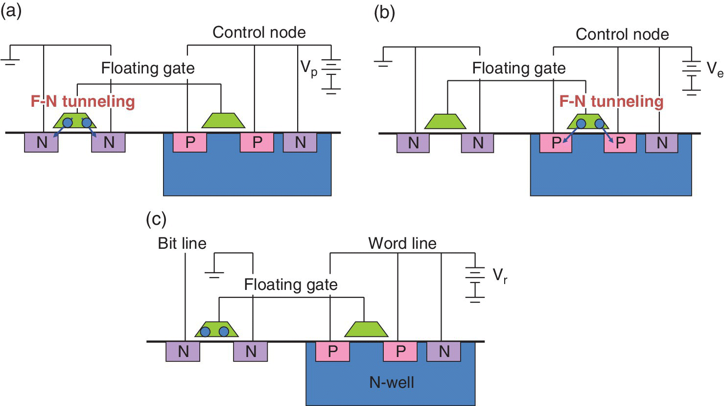
Figure 3.2 Schematic cross‐sections of single poly CMOS EEPROM cell with NMOS and PMOS transistors with electrically isolated common poly gate showing Fowler‐Nordheim (FN) program and erase: (a) program, (b) erase, and (c) read.
Based on K. Ohsaki et al. (IBM), IEEE Journal of Solid‐State Circuits, March 1994 [4].
A test chip was made in a 0.8 µm CMOS logic process. Write was done at V p = 15 V for 10 ms and erase at V e = 18 V for 100 ms. Cell size was 31 µm2. An analog circuit using this cell was also developed for use in a neural circuit.
Another single polysilicon embedded Flash memory cell in CMOS logic‐compatible technology was discussed by Bell Labs and Lucent Technologies in 2000 [5]. This 3 T cell was based on the IBM cell discussed in Ref. [4] but added a Fowler‐Nordheim tunneling erase gate and changed the control gate design to lower the cell threshold voltage. The cell could be made in a core CMOS logic process with only one additional masking step. It had the advantage of a low VDD read operation due to a lower erased‐state cell threshold and had lower gate voltage for programming. It also had higher endurance and longer data retention. Schematic circuits of the two cells are shown in Figure 3.3. Figure 3.3 (a) shows the IBM cell and Figure 3.3 (b) shows the Bell Labs cell.

Figure 3.3 Circuit diagram of two single poly embedded Flash cells: (a) IBM and (b) Bell Labs.
Based on R.J. McPartland and R. Singh (Bell Labs, Lucent), VLSI Circuits Symposium, June 2000 [5] (permission of IEEE).
For the Bell Labs cell, the erase gate voltage was 10 V. For the program the control gate voltage was 6.5 V with drain at 5.5 V and source at ground. Read had V ds at 1.5 V and the control gate voltage at 2.25–2.75 V. The cell was made in 0.25 µm technology using a 2.5 V logic CMOS process. Figure 3.4 shows a top‐down view of the layout of (a) the IBM cell and (b) the Bell Labs cell.

Figure 3.4 Top view of layout of (a) IBM 2T single poly EEPROM and (b) Lucent 3T single poly EEPROM with M3 erase gate added.
Based on R.J. McPartland and R. Singh (Bell Labs, Lucent), VLSI Circuits Symposium, June 2000 [5] (permission of IEEE).
In February of 2004, Virage Logic (now Synopsis) discussed a 130 nm fully CMOS logic embedded Flash memory, called a nonvolatile electrically alterable memory, intended for security code encryption [6]. This application required less than 16 K‐bits of nonvolatile memory and the macro size was competitive with that of a conventional double polysilicon embedded Flash array. The requirement to embed the memory in the logic circuit was based on security concerns for the code in discrete memory components being intercepted when the data crossed component pin boundaries. The cell was manufactured in a standard CMOS logic process with no special masks or additional process steps. It consisted of a coupling capacitor, a tunneling capacitor, and a PMOS read transistor all connected with a common floating polysilicon gate, as shown in the cross‐sectional view of the three transistor single polysilicon cell in Figure 3.5.

Figure 3.5 Cross‐section view of 3T single poly embedded Flash cell.
Based on J. Raszka et al. (Virage Logic), ISSCC, February 2004 [6].
All elements used a 7 nm oxide grown over the active areas compared to 10 nm for a conventional double polysilicon e‐Flash. There were no mask adders over a CMOS logic process or added process steps compared to seven mask adders for a standard double polysilicon Flash and 15 added process steps. Each bit was two memory cells connected in parallel and programmed with opposite data. A dedicated “compare” permitted use of a password and was used for security. The differential sensing permitted sensing signals less than 100 mV and the dual cell configuration increased yield due to the inherent redundancy. The programming voltage was supplied by an on‐chip high voltage generator that uses a closed‐loop regulation architecture involving three cascaded pumping states to attain 8 V and a special high voltage NMOS transistor with an NWELL source and drain, which was fully compatible with the CMOS process. The test chip contained a high voltage charge pump, which used a special high voltage NMOS device that was fully compatible with a standard CMOS process. The NMOS device is shown in Figure 3.6.

Figure 3.6 High voltage NMOS device fully compatible with standard CMOS process.
Based on J. Raszka et al. (Virage Logic), ISSCC, February 2004 [6].
To support the greater than 10 V breakdown voltage, capacitors were used with an area efficient metal–metal finger structure. The macro size was competitive with that of a standard double polysilicon embedded Flash memory. The electrical characteristics of the new single poly cell and those of a conventional double polysilicon embedded Flash in the same 130 nm process are shown in Table 3.3.
Table 3.3 Electrical characteristics of the new single poly cell and of eFlash.
| Electrical characteristics | Double poly | Single poly |
| Program time (ms) | 1.3 | 10 |
| Erase time (ms) | 25 | 10 |
| Read access time (ns) | 50 | 5 |
| 1 K‐bit macro size (mm2) | 1.3 | 0.9 |
| Retention time (years) | >10 | >10 |
3.2.3 Single Poly EEPROM Cells for Specialty Applications
A single polysilicon EEPROM cell for embedded memory integrated in a 130 nm RF‐CMOS process without extra masks or process steps was discussed by IHP Microelectronics in 1994 together with several Italian Universities [7]. The cell used an NMOS transistor and MOS capacitor sharing a floating polysilicon layer. The process also had high speed SiGe heterojunction bipolar transistors. A ±6 V supply was used for write/erase with F‐N tunneling. The cell operated at >1 ms, with endurance >103 cycles and >10 year data retention.
Early single polysilicon EEPROMs were also developed for specialty applications, such as the high temperature environments experienced by the MCUs used in automotive applications. In November of 1997, the Fraunhofer Institute in Germany discussed a single polysilicon EEPROM cell made in a silicon‐on‐insulator (SOI) technology known as SIMOX (Separation by IMplantation of OXygen), which used an oxygen ion beam implantation process on a silicon wafer followed by high temperature annealing to create a buried SiO2 layer under a thin film of surface single crystal silicon [8]. A single polysilicon EEPROM cell that worked at temperatures up to 250 °C was fabricated in 2 µm SIMOX technology with a film thickness of 120 nm using 40 nm gate oxide.
The single poly EEPROM process extension required only two additional masks and a few additional process steps which had the potential of being sufficiently low cost to use as an embedded memory in the automotive application. The two transistor cell used an NMOS select transistor and a floating gate transistor with 10 nm tunnel oxide. An issue was temperature‐induced leakage current in the select transistor at high temperatures. The control gate of the floating gate transistor was a separate n + diffused active area in the silicon film. Program and erase was by Fowler‐Nordheim tunneling current in the tunnel oxide at the injector drain. Cell size was 650 µm2, which was large but feasible if only a few K bits of capacity were required in the application. Only two additional masks were necessary for the EEPROM process module. The threshold window of an EEPROM cell with a capacitance ratio of 10:1 between the control gate and injector at 250 C °is illustrated in Figure 3.7.
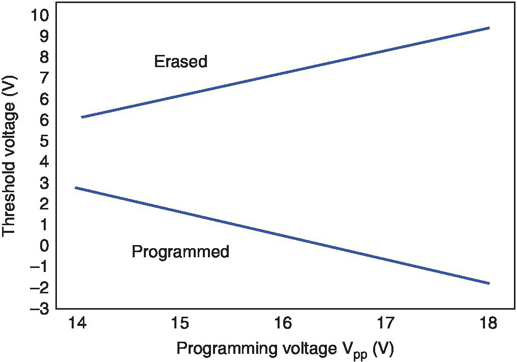
Figure 3.7 Threshold window of single poly EEPROM made in SOI Technology. Based on D. Gogl et al. (Fraunhofer Institute), IEEE Electron Device Letters, November 1997 [8].
ERASE was V cg/V sg = V pp and V s/V d = 0 V. Program conditions were V d/V sg = V pp and V sg = 0 V with the source floating. The threshold voltage was defined as the control gate voltage V cg necessary for a current of I ds = 1 μA at a drain bias voltage of V ds = 0.1 V. Endurance was about 105 program/erase cycles. The data retention test showed over 1000 hours at 250 °C.
In May of 2008, Tower Semiconductor discussed a low power single polysilicon logic NVM with an operating current less than 10 nA/cell and high program/erase speeds [9]. The memory was intended for use in logic with embedded memory in RFID and advanced mobile applications. No mask adders were required for a CMOS logic process. Programming and erase used Fowler‐Nordheim injection. Limitations were the use of up to 10 V for a 7 nm gate oxide required for program and erase, which resulted in diode leakage due to gate‐induced drain leakage (GIDL) in the periphery of the memory array.
A single poly EEPROM with a stacked MIM capacitor and n‐well was discussed by Chungbuk National University in January of 2009 [10]. The oxide capacitance in the n‐well region meant that the cell area and coupling ratio did not need to be sacrificed. The cell had a higher speed even though the cell size was small. Programming speed was nearly the same as a conventional MIM control gate and endurance was 10 000 program/erase cycles. The program threshold voltage shift was 1.4 V.
A 90 nm logic NVM Flash embedded in standard CMOS without a mask or process adder was described in 2011 by Genusion [11]. This cell was intended for use with RFID‐type applications. The charge was stored in the Si3Ni4 side spacer region of the CMOS transistor so that its charge loss process was not influenced by leakage current through the gate oxide or by surface leakage current on the side spacer. It was shown that the intrinsic retention capacity is more than 10 years at 125 °C after 10K cycling. The schematic cross‐sections in Figure 3.8 illustrate silicon nitride side spacer EEPROM operation for (a) the CHE program, (b) the avalanche HH erase, and (c) the read operations for the 90 nm logic NVM eFlash.

Figure 3.8 Illustration of silicon nitride side spacer EEPROM operation for (a) program by channel hot electron injection (CHEI), (b) erase by avalanche hot hole injection (AHHI), and (c) read.
Based on S. Shukuri et al. (Genusion), IMW, May 2011 [11].
The Flash element had an asymmetrical LDD structure constructed by using an I/O transistor in a 90 nm CMOS logic process. The source diffusion structure was optimized for channel hot electron injection (CHEI) to the side spacer for programming and avalanche hot‐hole injection (AHHI) for erasure without a mask adder or any process change. Read operation was done by applying 1 V to the drain.
A fully integrated HF‐band passive RFID Tag IC using 180 nm CMOS was described in 2011 by Kyun Hee University, the University of Texas, and eSilicon [12]. The target application was low cost security devices. An embedded 4 K‐bit EEPROM was used to support the Advanced Encryption Standard (AES) operation. Read and write accesses were performed using a 128‐bit wide buffer with self‐timed bursts made in a single polysilicon six‐metal low power 180 nm CMOS with a CoSi2 Schottky diode and an EEPROM process.
A low power embedded nonvolatile memory for use in a low cost RFID tag was discussed in 2013 by Ben‐Gurion University and TowerJazz [13]. The cell was a single polysilicon 4 T CMOS compatible Flash cell made into a 256‐bit rewritable NVM array. It was made in the TowerJazz 180 nm CMOS process using only standard logic process steps and masks. Static power for this cell during operation was 3.8 μW. A schematic of the cell structure is shown in Figure 3.9 (a) and a schematic circuit diagram of the cell is shown in Figure 3.9 (b). The memory was designed using the Cadence Virtuoso IC6 tool. Each block was designed, implemented, and verified through simulation using the “Spectre” circuit level simulator.

Figure 3.9 Single poly 4T cell in conventional CMOS showing (a) schematic drawing of the cell structure and (b) schematic circuit diagram of the embedded Flash memory cell.
Based on H. Dagan et al. (Ben‐Gurion University, TowerJazz), SISCAS, May, 2012 [13] (permission of IEEE).
An embedded nonvolatile memory for use in radio frequency identification (RFID) tags and near‐field communication (NFC) chips was discussed in 2016 by eMemory [14]. The RFID tag has a requirement for very low power and frequently used power harvesting from the UHF signal. The embedded NVM macro uses very low power and low voltage in both read and write. A standard CMOS logic process is used without any process or mask adders to reduce manufacturing cost. The single polysilicon EEPROM macro is used for both its low operating voltage and low power [15]. Existing CMOS logic devices were used in new design implementations to lower power. The chip supported an array density up to 4Kb, μW of operating power, and 10 K cycles of endurance. It was verified in 0.11 µm logic and in a low power process platform.
3.2.4 Multitime‐Programmable Single Poly Embedded Nonvolatile eMemories
Data‐retention mechanisms of logic embedded NVM in multiple‐time programmable (MTP) applications were discussed in 2013 by TSMC. These MTP cells have a cycling endurance that is less than the 10 000 cycles required of standalone nonvolatile memory. In April of 2013 TSMC discussed two mechanisms of data retention on logic embedded NVM in an MTP application [16]. Logic eNVM is commonly substituted for embedded Flash due to a faster time to market, logic compatibility, and the cost effectiveness of power management for MTP solutions.
Data retention of logic eNVM in bipolar, CMOS, DMOS, and HV technologies is not usually an issue due to the availability of thick tunnel oxide for the 5 V devices used in digital/analog ICs. The higher reliability requirements of the automotive application required a further understanding of the data‐retention mechanism for logic eNVM. A schematic cross‐section of the logic eNVM cell is shown in Figure 3.10 (a). The contact etch stop liner (CESL) covers the dielectric isolation oxide, which is on top of the floating gate. A schematic circuit diagram of the MTP unit bit‐cell is shown in Figure 3.10 (b). The cell is operated by a 5 V logic device with 12 nm tunnel oxide thickness. The capacitors controlling program and erase are PG and EG. Electrons are injected into the floating gate from PG while programming and ejected to EG while erasing.

Figure 3.10 Logic eNVM MTP cell: (a) schematic cross‐section and (b) schematic circuit diagram of a unit bit‐cell.
Based on Y.Y. Liao et al. (TSMC), IRPS, April 14, 2013 [16].
The data retention behavior of logic eNVM processed with thick tunneling oxide was studied and two new reliability mechanisms were considered. A physical data retention model was developed for this cell. Bit cell current (BCC) data‐retention degradation behaviors were studied for bake temperatures ranging from 25 to 250 °C. Larger degradation was found at higher bake temperatures or longer bake times. Retention degradation for the eNVM becomes gradually saturated with longer bake time due to the capacitive effect. The data‐retention degradation trend of the erase state after 10 000 program/erase (P/E) cycles is shown in Figure 3.11. At bake temperatures greater than 125 °C, the trend degrades and then recovers in later baking. For bake temperature less than 125 °C no recovery was observed. The chart of BCC degradation versus temperature dependence of the data retention bake is shown in Figure 3.11.

Figure 3.11 Logic eNVM cell data retention degradation trend of bit cell current in the erase state after 10,000 program/erase (P/E) cycles.
Based on Y.Y. Liao et al. (TSMC), IRPS, April 14, 2013 [16].
The model developed to explain this phenomena was that for the high temperature bake, the transconductance, G m, recovers faster after a 250 °C bake than after 125 °C. G m recovery was taken to indicate that electron traps generated near the Si substrate by P/E cycles can be detrapped from the tunnel oxide interface to the silicon substrate at high bake temperatures. A lower bake temperature does not have enough thermal energy to activate electron detrapping so no current recovery is observed.
Both thermally activated electron detrapping and data code program sequence can contribute to data‐retention degradation. Based on these results, low‐level Si–H compositions of CESL nitride were implemented to improved DR degradation.
Another MTP cell using a single poly CMOS EEPROM technology was discussed in 2013 by STMicroelectronics and the University of Brescia [17]. It was based on a new “half‐cell” structure, which was made in a conventional 130 nm CMOS process without an additional mask or process step. A test chip was made and characterized. This type of eEEPROM structure is targeted for embedding in SoC for applications such as IP security, RFID chips, analog trimming, postproduction customization, and display driver calibration. Such applications require a small amount of low cost NV memory that is programmable.
The cell is based on a new cell structure and a new design method. The new cell structure is a “half‐MOS” type of device, where the drain is removed from a MOS FET device. This reduces the tunneling gate capacitance (C tg). The half‐MOS cell reduces area, improves program and erase performance, and improves endurance. A schematic of a “half‐MOS” device is shown in Figure 3.12, with a schematic layout shown in Figure 3.12 (a) and a schematic cross‐section shown in Figure 3.12 (b). “Ed” and “Es” are active extensions below the poly of the drain and source sides. “Whm” is the width of the half‐MOS and “d” is the active polysilicon overlap length. In a MOSFET, Ed > 0 and Es > 0, whereas in a “half‐MOS”, Ed = 0 and Es > 0. A schematic circuit diagram of the “half‐MOS” 1.5 transistor MTP cell is shown in Figure 3.12 (c).

Figure 3.12 “Half‐MOS” device: (a) layout, (b) cross‐section and (c) cell schematic circuit diagram.
Based on F. Torricelli et al. (University of Brescia, STMicroelectronics), IEEE Trans. on Electron Devices, June 2013 [17].
During the program and erase, S, D, and PW are shorted, which forms the control gate terminal V cg and M1 functions as a coupling capacitor. During read, M1 is in transistor configuration and V tg = 3.5 V, V s = V pw = 0, and V d = 1 V.
The “half‐MOS” cell uses one of the smallest thin‐oxide tunneling capacitances available in conventional CMOS technology. It has good charge retention and endurance. The required area is reduced, but the control gate coupling ratio, endurance, and data retention are the same as a full MOS cell. A 130 nm CMOS test chip showed that the memory could be programmed and erased up to 10 000 cycles. The endurance did not depend on the tunneling capacitor area. The memory cell transconductance did not degrade with cycling. Data retention at 250 °C was shown.
In December of 2013, the University of Brescia and ST Microelectronics collaborated further on their “half‐MOS” single poly EEPROM cell with its program and erase per bit feature [18]. The cycling endurance was now improved to 10 000 cycles. The “half‐MOS” cell could be programmed and erased by Fowler‐Nordheim tunneling. The cell had a novel write inhibition method, which was enabled by a combination of the body effect of several “half‐MOS” devices. A 130 nm test chip was made and characterized. The “half‐MOS” bit‐cell cross‐section is shown in Figure 3.13.

Figure 3.13 “Half‐MOS” bit cell schematic cross‐section.
Based on F. Torricelli et al. (University of Brescia, STMicro), IEEE Electron Device Letters, December 2013 [18].
The “half‐MOS” device is an MOS transistor without the drain diffusion. An n‐type cell was used for nHM and a p‐type half‐MOS for pHM along with two MOS transistors, nM1 and nM2. The floating gate is the contactless polysilicon layer that is shared by nHM, pHM, and nM1. The cell is compatible with conventional CMOS technology and is programmed and erased by Fowler‐Nordheim tunneling. For the program (erase) the nHM (pHM) acts as a tunneling capacitor while the pHM (nHM) and nM1 are the control gate capacitors. During the program, electrons are injected into the FG from the channel of nHM. During erase, electrons are removed from the FG to the channel of pHM. For read, nHM and pHM are used as coupling capacitors and the drain current of nM1 is sensed. The transistor nM2 is the select transistor for the cell.
The single poly EEPROM cells were made in 130 nm CMOS with active‐poly overlap of the half‐MOS devices being 250 nm and bit‐cell area being 12.1 µm2. The single‐bit granularity does not use an additional area since the p‐type “half‐MOS” pHM is located in the n‐well separating the two p‐wells. Cycling endurance is 10 000 cycles and the V t window closes after 105 ms of write operations.
A two‐transistor embedded MTP memory cell in conventional CMOS technology was discussed in June of 2016 by Global Foundries, IBM, and UCLA [19]. An 80 K‐bit logic embedded multitime programmable memory macro was made using the two‐transistor cell. The cell uses a charge trapping mechanism in a 32 and 22 nm high‐k dielectric transistor in a standard logic process with no added process complexity.
Programming is accomplished by electron injection into the HiK gate dielectric present in a standard logic NMOS transistor. This is done by applying a word‐line (WL) voltage of 2 V (VPP), a source‐line (SL) voltage of 1.5 V, and grounding of the bit‐line (BL) at 0.0 V. This permits efficient trapping of electrons in the HfO2 interfacial layer, resulting in a threshold voltage (V th) increase. The V th shift found was 200 mV with a 10 ms programming pulse. This can be increased to 300 mV with a 100 ms pulse. The cell is erased by driving the word‐line (WL) to about –1 V and the SL to about 2 V. A single bit is stored in a twin cell, as illustrated in Figure 3.14.

Figure 3.14 Twin transistor memory cell using HiK logic NMOS process.
Based on J. Viraraghavan et al. (GlobalFoundries (Bangalore), IBM, UCLA), VLSI Circuits Symposium, June 2016 [19].
The cell is controlled by the WL, SL, BL true (BLt0), and bit‐line complement (BLc0). The V th of the NMOSt or NMOSc is shifted to store the data. WL drivers include a voltage switch to select between VPP and a main voltage VDD. The column decoder selects 1 of 4 BL pairs, which provides an 80 bit data‐line (DL) readout. An SL switch coupling to VSL1, VDD, and ground (GND) is provided per DL segment of four columns so that only the SLs in the selected segment are raised to VSL1 during programming and VDD during read while grounding the CLs in unselected DL segments. A preprogrammed indicator bit supports a default bit function in the macro. The 80Kb memory array was organized into 256 rows by 320 columns. This is scalable to a 14 nm FinFET technology.
3.2.5 Recent Single Poly Fully CMOS Embedded EEPROM Devices
A scalable logic gate nonvolatile memory device fabricated in a conventional CMOS logic process was discussed by FlashSilicon in October of 2014 [20]. The device was shown in 110 nm, 55 nm, and 40 nm nodes. Cell sizes for the NOR Flash array were defined by the process design rules of the CMOS logic nodes and ranged from 0.5425 µm2 in 110 nm technology to 0.1095 µm2 in 40 nm technology. The EEPROM cells were made of three MOSFET single poly logic floating gate devices processed in a conventional CMOS process. The original EEPROM device used the p‐MOS as the control gate, the CMOS logic gate as the charge storage floating gate, and the n‐MOS as the channel device. The device source/drain electrodes shared the same bit‐lines. A later version used an n‐type control gate embedded in the p‐type silicon substrate formed by an n‐implant or separated threshold and punch‐through implants from the n‐well implant module of p‐MOS devices in a CMOS process flow.
The minimum gate length for the logic core device gate formed the charge storage floating gate. A 6.5 to 8 nm oxide, which can hold the charges for the required retention time, formed both the tunneling oxide and coupling dielectric on top of the device channel and the n‐substrate control gate. Data retention tests were done with 110 nm CMOS logic process devices. The V t window was an average of 5.127 V. A 12 year data retention at 85 °C was achieved by baking for 24 hours at 250 °C.
The logic‐compatible EEPROM devices were integrated into a 6 T SRAM cell to form a nonvolatile (nv) SRAM (nvSRAM). They were also integrated into a nonvolatile register and a nonvolatile FPGA. The foundry for the embedded NVM devices was expected to be UMC, where 1 to 8 Mb density devices were being developed in 40 to 55 nm processes.
A model for a single polysilicon EEPROM cell was developed by the National University of Defense Technology of China in October of 2014 [21]. This model provided an expression for the floating gate potential. By combining this model and the gate current data for the tunneling transistor, a method was found to do the transient simulation of the memory cell. This simulation included program and erase operations. An extension to the model was developed to enhance the model’s universality. The results of simulations using the model appear to have better consistency with the TCAD simulation results than those using the traditional model. This new model is expected to be useful for the design, evaluation, and optimization of a single poly EEPROM cell.
A scalable single polysilicon eEEPROM with a tungsten (W) control gate in a full CMOS process was discussed in April of 2015 by the National Tsing Hua University (NTHU) [22]. The single polysilicon structure had a low manufacturing cost, low process defects, and short turnaround time since it was fully compatible with a CMOS process. A single poly EEPROM with a W control gate had lower control gate (CG) resistance, no parasitic polysilicon depletion, and smaller drain‐induced barrier lowering (DIBL) due to the metal CG. Its fringing capacitance enhanced the coupling ratio and increased the program/erase window compared to a cell coupled by a poly finger structure.
A metallic tungsten (W) CG cell with a select gate (SG) transistor control and various spacings from CG to floating gate (FG) was studied. It was shown that reducing the spacing from CG to FG could decrease cell size without any performance degradation. This cell could be integrated in an advanced CMOS SoC due to its scalability, simple design, and good isolation between the W CG and the FG, when made in a full CMOS process. The 130 nm CMOS cell consisted of a 3.3 V n‐MOSFET for a read transistor connecting with a polysilicon finger as FG and was coupled with the surrounding W finger as W‐CG. The selected bit in the W‐CG EEPROM array was programmed by channel hot electron injection (CHEI) and was erased by Fowler‐Nordheim (FN) tunneling.
The performance of this single polyEEPROM cell with a W‐finger coupling structure was compared to that of a conventional polysilicon‐finger coupling cell, also in 130 nm CMOS, in September of 2014 by NTHU [23]. A schematic cross‐section of the P‐finger cell and the W‐finger cell is shown in Figure 3.15. The major coupling capacitances and potentials are indicated.

Figure 3.15 Schematic cross‐section of (a) P‐finger coupling cell and (b) W‐finger coupling cell.
Based on C.P. Chung et al. (NTHU), IEEE Trans. on Electron Devices, September 2014 [23].
The W‐finger coupling cell was shown to have a smaller drain‐induced barrier lowering (DIBL) effect, a higher coupling ratio, and a high cell current and P/E speeds as a result of its metallic control gate and the incremental capacitance from the control gate structure. Reliability characteristics were comparable between the two cells. The W‐finger coupling cell had a wider P/E window during reliability tests.
A new single poly EEPROM cell in conventional CMOS intended for medium density applications was discussed in October of 2015 by the University of Brescia [24]. A schematic cross‐section of the proposed single poly EEPROM cell is shown in Figure 3.16. A pMOS tunneling device is used for programming and erase and an nMOS transistor is used for read and for selecting the memory cell. The pMOS device is a minimum sized transistor that uses the gate oxide of the I/O transistors in the process. This improves the coupling capacitance, minimizes the area, and guarantees the retention. The cell is programmed by band‐to‐band hot electron injection (BBHEI) and erased by Fowler‐Nordheim tunneling. The writing method used requires only a single triple well, which reduces area and ensures fast, reliable operation. The nMOS transistor (nM1) is used for sensing the drain current of the cell during the read operation and as a control gate capacitor during the write operation. The capacitive coupling ratio is CnM1/(CpM1 + CnM1).

Figure 3.16 Single polysilicon EEPROM cell made in conventional CMOS with pMOS tunneling device used for programming and erase, and nMOS transistor used for read and select.
Based on L. Milani et al. (University of Brescia), IEEE Trans. on Electron Devices, October 2015 [24].
The nMOS transistor (nM2) is used to select the memory cell. The FG is the uncontacted polysilicon gate shared by pM1 and nM1. For program, the diode is reverse biased and the BBHEI mechanism is enabled. The hot electrons generated are injected into the FG. During erase, both NW and TG are biased at high voltage, which leads to FN tunneling. During read, the drain current of nM1 is sensed; nM2 is required to select the cell in the array.
The efficiency of the write operation and the reliability are based on a new pMOS tunneling device. A schematic cross‐section of this device is shown in Figure 3.17. P+ is the high doping implant. The floating gate (FG) is not silicided since it is covered by a mask, which enhances the reliability of the device.

Figure 3.17 Schematic cross‐section of pMOS tunneling device.
Based on L. Milani et al. (University of Brescia), IEEE Trans. on Electron Devices, October 2015 [24].
The memory cell was programmed in 1 ms at V p = –5 V and erased in 10 ms at V e = 18 V. This was taken to confirm that the BBHEI tunneling is faster than the FN tunneling. BBHEI was shown to be 1000 times more efficient than CHEI. The maximum BBHEI is achieved with a programming voltage V p = V dd, which ensures low power operation.
The cell was made in a 180 nm CMOS process. The memory cell area is 5.91 µm2. It could be programmed in 1 ms and erased in 10 ms. It could be cycled >10 k times with a voltage window greater than 2 V. It guaranteed the data retention and enabled reliable programming and erase with a single triple well. The technology limited V p < V dd so charge pumps are not needed for programming. The program and erase characteristics are temperature independent. This cell enables large parallel data writing, fast memory operations and test time reduction. It is suitable for moderate density and low cost applications.
3.2.6 Single Polysilicon eNVM in High Voltage CMOS
MCU for high voltage CMOS applications are also required with small amounts of low cost CMOS compatible nonvolatile memory (NVM). In March of 2014, SK Hynix discussed a select gate lateral coupling (SGLC) embedded NVM, which added no steps to a 90 nm high voltage CMOS process [25]. The select gate (SG) of the new cell is designed to function as both a control gate (CG) and an SG using only lateral capacitance coupling. The cell is relatively small, free of over‐erase and has multiprogrammable features. It is programmed by channel hot electron injection (CHEI) and erased by band‐to‐band tunneling‐assisted hot hole erase (BTBT HHE). This results in a 20 µs program and 100 ms erase. Erase time is 4.5 ms at V erase = 12 V. Over 3 V threshold voltage window is possible after 500 cycles and 10 year data retention is estimated at 85 °C. A schematic circuit diagram of the cell is shown in Figure 3.18. The select gate (SG) controls the floating gate (FG) by lateral capacitive coupling.
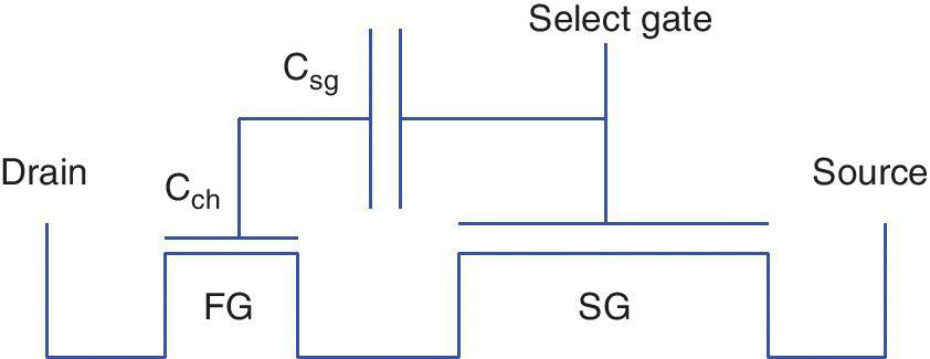
Figure 3.18 Schematic circuit diagram of select gate lateral coupling (SGLC) eNVM cell where C ch is the floating gate (FG) to substrate capacitance and C sg is the FG to select gate (SG) lateral capacitance.
Based on S.K. Park et al. (Hynix), IEEE Electron Device Letters, March 2014 [25].
The operation of the cell uses lateral capacitance coupling between the gates of neighboring cells. An SG and an FG are adjacent to each other and the coupling energy between the two is used for a floating gate. Since the select gate is also a control gate, the double poly can be eliminated along with ONO dielectric processes. C sg is the lateral spacer capacitance between SG and FG and C ch is the vertical capacitance between the FG and the substrate.
A test chip for the cell was made in 90 nm high voltage CMOS (HVCMOS). This process had 1.2, 6, and 32 V transistors. A 1.2 V junction was used in a 6 V gate oxide SGLC cell. Usually, the 1.2 V LDD implant is blocked on the thick gate oxide area. The cell, however, used a 1.2 V logic LDD junction as a program junction for the NVM. The cell used CHEI and BTBT HHE, which permits a lower bias than FN tunneling. The coupling ratio of C sg/C ch was >70%. The coupling ratio was primarily governed by the SG to FG space, with a smaller space producing a high coupling ratio. For this reason the SGLC cell was expected to be scalable.
The V t window of the programmed and erased cell is over 3.0 V. It was shown that with the same read bias as a gate bias of 3.3 V, the programmed cell current is 2.5 nA and the erased cell current is over 27 μA. This large current difference made it possible to easily distinguish the programmed cell from the erased cell. Since the BTBT hot hole erase causes more oxide degradation than FN erase, the SGLC cell was developed for code storage applications that do not require high endurance. Using a single poly process with a select gate length of 0.2 µm the tested cell was 1.34 µm2, which is comparable to the size of a 6 T SRAM in the same technology.
A byte alterable high voltage CMOS logic‐compatible EEPROM was discussed in May of 2014 by Genusion [26]. The EEPROM was made in a 90 nm Flash process with a three transistor AND‐type unit cell intended for disturb‐free operation. The device used back‐bias assisted band‐to‐band tunneling hot electron injection (B4‐HE or BBHEI) for programming and Fowler‐Nordheim tunneling for erase. A single pulse program and erase cycling was confirmed up to one million cycles using 10 µs program and 1 ms erase; 10 year data retention was shown at 150 °C. In an array, the unit cell size was 57 F2, which is half of conventional EEPROM at 80 F2 to 100 F2. The unit cell consists of three transistors in series using an AND array architecture.
This byte alterable BBHEI EEPROM had reliable operation and ease of implementation in a logic fab. The two transistors on both sides of the memory transistor are pass transistors, which are p‐channel floating gate contacted transistors. The pass transistors control the voltage of the source and drain of the memory transistors to achieve disturb‐free operation. An n‐channel memory gate select transistor is connected to every 1 byte of memory cells to control the memory gate. Enhancement and depletion operation of the cell is done for the read gate voltage of 0 V.
Key features for a 1 MB device are as follows. Standby current is 1 μA. Program speed is 10 µs with current of 3 mA, erase speed is 1 ms with current of 3 mA, and read speed is 20 ns for I cc = 10 mA. The cell is easy to make in an existing high voltage CMOS (HVCMOS) process.
3.3 eFlash Cells Using Multiple Single Polysilicon CMOS Logic Transistors
Embedded Flash cells can be made using only the CMOS logic transistors that exist in the standard CMOS process without process changes.
In June of 2012, the University of Minnesota described a five (5) transistor logic‐compatible single poly embedded Flash memory that used no special devices other than a standard CMOS core and I/O transistors. A 5 T embedded Flash memory cell used a selective row refresh scheme for improved endurance [27]. It was made in a low power standard logic process with 5 nm tunnel oxide and no process adders above conventional LPCMOS. An overstress‐free high voltage switch enlarges the V th window by greater than 170%. A schematic circuit diagram of the 5 T cell is shown in Figure 3.19.

Figure 3.19 Schematic circuit diagram of 5T logic compatible single poly embedded Flash cell.
Based on S.H. Song et al. (University of Minnesota), VLSI Circuits Symposium, June 2012 [27].
This 5 T single poly eFlash technology in conventional CMOS logic uses CMOS I/O devices and can serve as secure on‐chip NVM storage for chips built in a conventional logic process. All five transistors in the cell are made using standard 2.5 V IO transistors with an oxide thickness of 5 nm. The width of M1 is eight times wider than M2 or M3 to achieve a high coupling ratio for improved erase and program. M1 and M2 are PMOS transistors and M3 is an NMOS transistor.
The 5 T cell can be used for adaptive self‐healing techniques for reducing the effects of process variation and circuit aging for system information retained for long periods of time. It can also be used for zero‐standby power systems by saving critical data during power‐down without adding cost to the process technology. An overstress‐free high voltage switch and selective WL refresh method are used for an improved cell V t window and higher endurance.
A new high voltage switch (HVS) was used with the 5 T cell. The previous switch had a maximum allowable program and erase voltages limited to two times the nominal I/O voltage due to gate oxide reliability concerns. An issue with the previous switch was that the internal node voltage in the PMOS cascode was sensitive to the V t drop of the PMOS device, which made the circuit susceptible to the effects of variation and also limited the output voltage range. The new HVS had a maximum allowable program and erase voltage that was up to four times the nominal I/O voltage and provided robust output voltage levels. Technology features for the 65 nm 5 T single poly eFlash cell macro include a 5 nm oxide thickness, 1.9 V V th window, erase time of 1 ms, program and read time of 10 µs and 8.62 µm2 cell size in 65 nm technology.
Erase and program of the 5 T configuration macro are illustrated in Figure 3.20. The erase bias is shown in Figure 3.20 (a). The program bias is shown in Figure 3.20 (b), with the neighboring cell having programming inhibited using a self‐boosting bias.
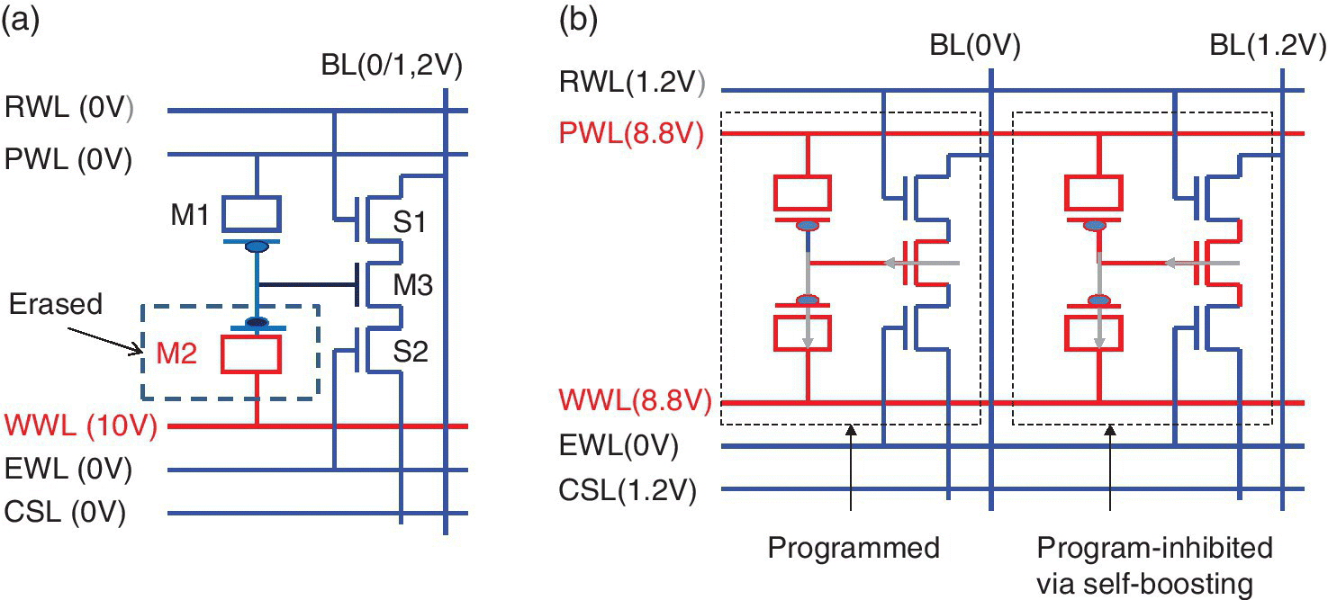
Figure 3.20 5T configuration macro: (a) erase bias and (b) program bias with neighboring cell having program inhibited via self‐boosting.
Based on S.H. Song et al. (University of Minnesota), VLSI Circuits Symposium, June 2012 [27].
An earlier single poly 3 T PMOS eFlash cell was compared to the circuit diagram of the 5 T eFlash cell by the University of Minnesota in May of 2013 [28]. The circuit diagrams of the 3 T cell and the 5 T cell are shown in Figure 3.21. Both cells have been made in 65 nm conventional CMOS logic. Tunnel oxide for both was 5 nm and both used Fowler‐Nordheim tunneling for program and erase. Write voltage for the 3 T cell was 8 V but 5–10 V for the 5 T cell. Write power was low. The 5 T cell offers the advantage of no erase disturb of unselected WLs. Data retention for the 5 T cell was >486 hours at 27 °C and cell size was 8.62 µm2 drop phrase “or (2111 F2)”.

Figure 3.21 Schematic circuit diagram of 65 nm single poly (a) 3T eFlash cell compared to (b) 5T eFlash which eliminates erase disturb.
Based on S.‐H. Song et al. (University of Minnesota, Samsung), IEEE Journal of Solid‐State Circuits, May 2013 [28].
Compared to the single poly 3 T cell, the single poly 5 T cell has a larger V th window, single word‐line program, fast read time, and a much smaller cell size. The cell size of the dual polysilicon cell is smaller, but the dual poly process is more complex. The capacity of the 3 T and 5 T single poly cells are similar and smaller than that of the dual poly Flash cell.
In April of 2013, the University of Minnesota discussed the technology of the n‐channel and p‐channel single poly floating gate embedded Flash memory cells made in a conventional CMOS logic process [29]. These three transistor single poly devices have their floating gates coupled to net the voltage required for program and erase without a high voltage actually being applied at any point. They were made in PMOS‐NMOS‐PMOS in a deep n‐well.
A conventional double poly or split gate eFlash requires process overhead for the floating gate and also requires high voltage (>14 V) transistors. Single poly eFlash has no process overhead since it uses conventional CMOS logic I/O devices. A schematic cross‐section of a p‐channel 3 T single poly eFlash that is configured for the erase operation is illustrated in Figure 3.22. For erase there is electron FN tunneling into the FG in transistor M2 under the coupling influence of –7.6 V on the WWL and 1.2 V on the PWL, while the source and drain of the FG device float. This is a net erase voltage of 8.8 V.

Figure 3.22 Erase of P‐channel 3T single poly eFlash cell with Fowler‐Nordheim electron tunneling into the floating gate of M2.
Based on S.H. Song et al. (University of Minnesota), IRPS, April 2013 [29].
A schematic cross‐section of the p‐channel 3 T single poly eFlash configured for the program operation is illustrated in Figure 3.23. For programming there is electron FN tunneling from the FG in the PMOS M3 with the FG at 6.6 V and the PWL and WWL at –7.6 V for a net coupled programming voltage of 14.2 V.

Figure 3.23 Programming of P‐channel 3T single poly eFlash cell with electron Fowler‐Nordheim tunneling from the floating gate of M3.
Based on S.H. Song et al. (University of Minnesota), IRPS, April 2013 [29].
There are several reliability effects to consider. Disturb during programming is one such reliability issue. Figure 3.24 shows schematic circuit diagrams of program and erase configurations for the p‐channel 5(2 + 3)T single poly eFlash cells using electron Fowler‐Nordheim tunneling.

Figure 3.24 5T schematic circuit diagrams of the P‐channel single poly P‐channel macros with applied (a) erase bias and (b) program bias with program inhibited via self‐boosting.
Based on S.H. Song et al. (University of Minnesota), IRPS, April 2013 [29].
For the bias conditions of a cell being programmed, the boosted channel voltage should be high with suppressed subthreshold and junction leakage current to prevent program disturb in an unselected cell. The select transistor uses a longer channel length to minimize subthreshold leakage of the boosted channels. The self‐boosting technique in a conventional logic technology permits row‐by‐row program/erase array architecture without a disturb issue in the unselected WL cells.
The feasibility of multilevel cell programming was investigated and the 5 T eFlash cells showed four distinct states with a sensing margin of 0.4 V for 150 °C baking temperature and 100 P/E pre‐cycle. For the n‐channel 5 T and p‐channel 5 T eFlash, supply voltage was 1.2 V for the core and 2.5 V for the I/O. Tunnel oxide was 5 nm and cell size was 8.62 µm2.
A 6 T eFlash memory cell was proposed by the University of Minnesota in August of 2014 [30] and in September of 2013 [31] for a bit‐by‐bit rewritable eFlash memory in 65 nm logic process. This cell improved the overall cell endurance by eliminating redundant program/erase cycles without disturbing cells on unselected word‐lines. A multistory high voltage switch used four boosted supply levels generated by a compact voltage doubler based on an on‐chip negative charge pump. Schematic circuit diagrams are shown in Figure 3.25 of (a) the original 5 T eFlash and (b) the new 6 T eFlash.

Figure 3.25 Schematic circuit diagrams of (a) original 5T eFlash and (b) 6T eFlash with improved endurance.
Based on S.H. Song et al. (University of Minnesota), Custom Integrated Circuits Conference, September 22, 2013 [31].
In order to improve the overall cell endurance characteristics the array is capable of writing data on a bit‐by‐bit basis without using boosted BL voltages. To enable a bit‐by‐bit write, the cell boosts the FG of each cell selectively using preferential coupling. The cell does not share the source and drain node between adjacent cells in the WL direction, which permits it to have different voltage levels for each bit‐cell in the same WL. The FG node voltage difference can be used for the bit‐by‐bit write operations.
Differences between the two cells included: cell size of 5.62 µm2 for the 5 T and 15.3 µm2 for the 6 T. The capacity of the 6 T at 4Kb was double that of the 5 T at 2Kb. Write voltage for the 5 T was 10 V and for the 6 T was –7.2 V. Both cells were in 65 nm logic and had 5 nm tunnel oxide. While the capacity of the 6 T cell macro is doubled, the write voltage is reduced but the cell size more than doubles.
A further comparative study of the 5 T single poly eFlash cell was conducted by the University of Minnesota in November of 2014 [32]. Characteristics of the different single poly eFlash memory structures compared were: memory disturbance, program/erase speed, endurance, and retention. They concluded that the 5 T eFlash memory cell structure was the most attractive option for logic‐compatible eNVM.
3.4 Split Gate Technology for Floating Gate Embedded Flash
3.4.1 Early Split Gate Embedded Flash Floating Gate Technology
The 1.5 transistor (1.5 T) split gate floating gate Flash technology for use in embedded Flash memory was developed early and is widely used in foundries. The split gate has the advantage over the stacked double poly standalone 1 T Flash of a fast simplified erase at the cost of additional silicon and processing.
An early split gate embedded EEPROM application was discussed by Analog Devices in December of 1998 [33]. The SoC chip was an IEEE 1451 standard transducer interface module with an embedded Flash memory for storing transducer identification, calibration, correction data, and manufacturer‐related information. The chip integrated an eight‐channel 12‐bit ADC, two 12‐bit DAC, and an 8‐bit MCU with 256bytes of SRAM and a 10.5KByte Flash EEPROM. A split gate Flash EEPROM cell was used, which had poly‐to‐poly erase and metal‐to‐poly capacitors with a calibration algorithm in the ADC [34]. The 27.5 mm2 chip was made in 0.6 µm CMOS. It operated from 2.7 to 5.5 V and dissipated 13 mA of active current at 3 V/12 MHZ. An illustration of a schematic cross‐section of the split gate Flash EEPROM cell is shown in Figure 3.26.

Figure 3.26 Cross‐Section of split gate Flash EEPROM cell.
Based on T. Cummins et al. (Analog Devices), IEEE Journal of Solid‐State Circuits, December 1998 [33].
The conventional stacked double poly EEPROM process provides a high capacity memory device but requires: extra layers for the floating gate, high voltage devices, deep implants for HV devices, tunnel oxide, and extra drain implants for erase. Over‐erase prevention could require extra logic or a state machine controller. On the other hand, single polysilicon cells simplify the memory process, making it more compatible with CMOS logic, at the expense of a much larger cell size, which makes the integration of a large number of bits unfeasible.
A split gate EEPROM cell with poly‐to‐poly erase is a compromise between the high process complexity of the conventional EEPROM and the large cell size of the single polysilicon EEPROM. The thick oxide erase mechanism means that no tunnel oxide or drain engineering is required for erase, which simplifies the process. Both the cell program and erase operations are self‐limiting, which eliminates the requirement for over‐erase prevention circuitry.
The split gate EEPROM cell with poly‐to‐poly erase was patented in 1993 by Silicon Storage Technology [34]. Erase and program operations are shown in Figure 3.27. Erase, shown in Figure 3.27 (a), is by thick oxide poly‐to‐poly Fowler‐Nordheim tunneling of electrons from the poly1 floating gate to the poly 2 control gate and (b) program, shown in Figure 3.27(b), is by channel hot electron injection (CHEI) from the source to the floating gate.

Figure 3.27 Cross‐section showing (a) erase and (b) program of split gate cell.
Based on B. Yeh, US Patent 5 242 848, September 7, 1993 [34].
A 65 nm embedded split gate Flash memory embedded in a conventional CMOS logic process technology was discussed by TSMC in April of 2011 [35]. A cross‐sectional view of the split gate cell is shown in Figure 3.28. This cell uses source side injection (SSI) for programming and poly‐poly Fowler‐Nordheim tunneling for erase. The structure has multiple floating gate dielectrics. This memory does not have the limitations of the stacked gate Flash, which include scaling limitations due to the gate control oxide acting as tunnel oxide and due to drain turn‐on program disturb.

Figure 3.28 Schematic cross‐section of the 65 nm split gate Flash cell with SSI program and poly‐to‐poly Fowler‐Nordheim erase.
Based on Y.S. Chu et al. (TSMC), IRPS, April 10, 2011 [35].
This cell showed good scalability due to the erase tunnel oxide being decoupled from the floating gate oxide. It had good program disturb immunity since the select gate (WL) could turn off the channel of unselected cells. It did not need the boosted WL voltage during read access that the stacked gate Flash used. This resulted in comparative savings of power and access latency. The process was simplified by forming the FG self‐aligned to the control gate (CG). Typical operating voltages for a 65 nm split gate Flash cell are given in Table 3.4.
Table 3.4 Typical operating voltages for a 65 nm split gate Flash cell.
| CG | EG | WL(SG) | CS | BL | |
| Program | 11 | 1 | 1.3 | 5 | 0.2 |
| Erase | 0 | 13 | 0 | 0 | 0 |
| Read | 1.8 | 0 | 3.3 | 0 | 1.3 |
A 256Kbit data Flash macro and a 16Mb code Flash macro were made to demonstrate that automotive grade embedded Flash could be made in 65 nm CMOS using seven added masks. The automotive grade data Flash memory was made with 100 K cycle endurance, 10 year data retention at 125 °C, and reliability at 1 ppm. The code Flash showed 10 000 cycle endurance. A comprehensive dielectric screen methodology was shown. Both erase time push‐out and the dominant mechanisms of data retention were studied.
A split gate Flash memory cell embedded in a 65 nm high performance CMOS logic process with copper interconnects and low‐k dielectric were discussed in May of 2012 by Infineon and TSMC [36]. The cell used a self‐aligned process and had a gate spacer used during processing. The cell had good reliability and only one additional mask used for the split gate structure over the usual stacked gate process. The process flow was modular with both high voltage and Flash sections. The high voltage transistors required additional wells and thick gate oxide with special implants and LDD junctions. They were made in the same poly layer used for the floating gate. A third thick poly layer was used to form the select gate (SG) spacer. A schematic cross‐section of the cell is shown in Figure 3.29.

Figure 3.29 Schematic cross‐section of split gate Flash cell in 65 nm high performance CMOS logic.
Based on D. Shum et al. (Infineon, TSMC), IMW, May 2012 [36].
The cell was optimized for minimum module area overhead and high endurance. It could be integrated as a module in a standard stacked gate technology. The cell was proposed for high performance automotive CMOS logic and for smart card applications. A 2MB 65nm Flash automotive product demonstrator with 2MB of SRAM and a 32KB of ROM was designed and tested. The use of a Flash cell process self‐aligned to the stacked gate process allowed for scaling the cell without encountering lithographic limits or adding additional masking layers.
Low power embedded Flash in MCU is used in such applications as touch control ICs, smart meter controllers, and wireless connectivity. For such low density applications, 350, 250, and 180 nm process node technologies were in volume production at TSMC in May of 2013 [37]. The embedded Flash in these products was a first generation split gate cell. For higher density 2–16 Mb embedded Flash MCU applications, a new split gate cell was used in 90 and 55 nm low power (LP) processes in 12 inch wafer fabs. This technology was targeted at a wider range of applications in the automotive, industrial, and commercial markets.
The new split gate cell had fast code execution and was expected to serve automotive applications better. A new single‐ended sense amplifier (SA) was implemented on a 2Mb split gate eFlash in the 90 nm low power (LP) process. In 55 nm technology, the split gate Flash had a read speed up to 125 MHz using a single‐ended sense amplifier (SA), but maintained a low power read at 75 μA/MHz. This cell used a five‐metal eFlash IP made in a 90 nm LP process. It had up to 10 k cycle endurance in automotive applications. It was expected that the new split gate Flash cell with the new SA would primarily be used in the 55 nm technology.
High performance mobile processors and MCUs require large capacity, fast‐read embedded nonvolatile memory (eNVM) for code and data storage. Since conventional current‐mode sense amplifiers (CSA) cannot achieve fast random read access time due to significant summed read‐path input offsets, in November of 2013, NTHU, Shou University, and TSMC proposed an asymmetric voltage‐biased CSA to suppress summed read‐path input offsets and enable high speed sensing without run‐time offset‐cancellation operations [38]. A 1Mb eFlash macro with BL‐length test modes was made. A conventional split gate eFlash cell macro was used for the eNVM. This macro had 3.9 ns random read time. Features of the 90 nm low power split gate embedded Flash included: 1.2 V power supply, 512 cell bit‐line length, and random read access of 3.9 ns at 1.2 V typical. Area overhead was less than 1%, read power overhead was less than 2%, and test time overhead was less than 0.5%.
A split FG Flash cell with corner enhanced poly‐to‐poly tunneling was announced in January of 2012 by Silicon Storage Technology, now Microchip, and SST described its first three generations of memory cell [39]. These split gate memory cells used source side hot electron injection for programming and Fowler‐Nordheim poly‐to‐poly tunneling for erase. The first two generations had an intentionally sharpened floating gate tip formed using local FG oxidation. This made it possible to use a relatively thick tunnel oxide, which reduced such reliability issues as stress‐induced leakage current and program erase cycling‐induced data loss.
Schematic cross‐sections of the SST split gate cell are shown in Figure 3.30. Figure 3.30 (a) illustrates the first generation 1.2 µm to 130 nm technology cell. Figure 3.30 (b) illustrates the second generation 250 to 130 nm technology cell, which used a triple self‐aligned process. The FG was self‐aligned to the shallow trench isolation and the source line and word line poly were self‐aligned to the floating gate. The FG tip curvature was achieved by using reactive ion etching. Figure 3.30 (c) illustrates the third generation cell, which had a dedicated erase gate so the word‐line oxide was not stressed during erase and could be scaled. A separate coupling gate was used for positive biasing of the FG during programming and the source line to floating gate overlap was eliminated.
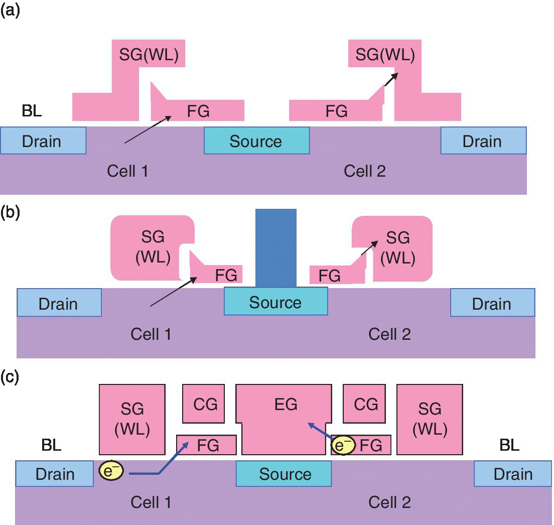
Figure 3.30 SST split gate “Super” Flash. Illustrations of (a) first generation, (b) second generation and (c) third generation technology cells.
Based on Y. Tkachev (Silicon Storage Technology), IEEE Trans. on Electron Devices, January 2012 [39].
The F‐N poly‐to‐poly erase of the first generation cell is from the floating gate to the poly SG (WL) and is at 12–14 V. Programming uses SSHEI from the floating gate through the tunnel oxide to the drain and the SL is at 8–10 V.
For the third generation cell the F‐N poly‐to‐poly erase is from the floating gate to the erase gate (EG) with the EG at 11 V and the other gates at 0 V. SSHEI programming is from the floating gate through the tunnel oxide to the drain, with the coupling gate (CG) at 10.5 V and the SL and EG at 4.5 V. The use of the CG permitted a reduction in the source voltage during programming, which reduced the programming‐induced degradation of the cell channel and improved program erase cycle endurance.
Reduction of program‐induced degradation for the split gate Flash was discussed in March of 2014 by SST [40]. The degradation mechanism was induced by program‐erase cycling in a split gate memory cell. A test structure was used that had two cells with a common floating gate. This test structure permitted separation of the degradation mechanisms, which occurred in the floating gate oxide and in the tunnel oxide during cycling. It was shown that the program‐induced floating gate oxide degradation became less significant for more advanced technologies that use lower programming voltage.
The cycling‐induced degradation of erase performance was found to be caused by electron trapping in the floating gate oxide during programming and in the tunnel oxide during erase. It was shown that the third generation cell had a significantly smaller program‐induced degradation than the first generation due to the lower source voltage used in programming.
3.4.2 Issues, Peripherals, and Applications‐Specific FG Split Gate Memory
A 45 nm logic compatible 4Mbit triple poly splitgate cell embedded Flash was discussed in May of 2014 by Samsung [41]. This device was intended for applications such as smartphones with security features, near‐field communications (NFC), banking, transportation pass, and ID. The memory capacity requirement was from 1 to 16 Mb. Some of the specifications of the various applications targeted are shown in Table 3.5.
Table 3.5 Various application specifications for split gate Flash chips. Based on Lee et al. [41].
| Characteristics | Smart card | General MCU | Automotive MCU |
| Endurance (k‐cycles) | 100–500 | 10–100 | 100 |
| Retention (years) | 10 | 10 | 10 |
| Temperature (°C) | –40 to +85 | –40 to +85 | –40 to +125/+150 |
| Read speed (MHz) | >20 | >25 | >75 |
A schematic cross‐section of the 45 nm logic compatible triple polysilicon split gate cell is shown in Figure 3.31. Scaling to 45 nm technology was accomplished by forming a shallow source‐line junction and by using thin gate oxide in the WL transistor. A low voltage word‐line (WL) transistor was used without WL boosting. The use of a separate control gate permitted source‐line voltage to be reduced so that program power could be reduced. The lower program power and low voltage WL meant the charge pump design could be simplified, which resulted in size reduction. The process flow for the 45 nm 1.5 T Flash involved making the cell first. The logic transistor‐related modules were processed after cell and high voltage (HV) module formation.

Figure 3.31 Schematic cross‐section of 45 nm logic compatible triple poly split gate cell.
Based on Y.K. Lee et al. (Samsung), IMW, May 2014 [41].
Process integration was designed for logic compatibility so that existing IP could be used. The chip had 40 MHz read access, program time of 25 µs, and erase time less than 2 ms. Endurance was 1 M cycles and data retention was 10 years. The good endurance resulted from strong localization of the tunneling process and suppression of hole injection in the FG corner. Good retention was shown at 150 °C. Immunity to disturbance at low program power was verified. The poly‐to‐poly erase operation decoupled unselected cells, resulting in immunity to disturb.
A configurable logic array test structure was discussed in March of 2013 by SST [42]. The chip was developed using a split gate Flash memory cell configuration element (SCE) in 90 nm embedded Flash technology. The SCE eliminated the requirement for special fabrication processes and SRAM circuits and reduced the configuration time for the programmable array. The configuration element was created using twin split gate Flash cells. The cell used poly‐to‐poly erase and source‐side‐channel hot‐electron injection programming. The SCE technology eliminated the triple‐well process requirement. A schematic circuit diagram of the split gate Flash SCE and programmable array switch is shown in Figure 3.32.

Figure 3.32 Split gate Flash SCE and programmable array switch.
Based on H. Om'mani (Microchip/Silicon Storage Technology), ICMTS, March 2013 [42].
The Flash‐based element used the same operation as used in the memory cell. Acceptable erased and programmed cell currents were achieved during the SCE Flash mode. The switching logic array (SLA) configuration can fully transmit the VDD signal without degradation to the output through the memory element. The cell current measured in Flash mode for the erased cell is around 27 μA and for a programmed cell is less than 10 pA.
A binary code inversion technique was used for an embedded Flash memory sense amplifier, which reduced the read current. This technique was discussed in May of 2014 by KAIST [43]. An original binary code was programmed into the Flash memory with an inverted binary code‐based bit inversion technique. The de‐inversion hardware was implemented with small logic gates to restore the original binary data so only logic current was consumed rather than analog sink current in the sense amplifier. The proposed technique was evaluated using a 128KB Flash memory embedded in an MCU made in 180 nm EEPROM technology. The circuit level simulation result showed that a fresh chip with the proposed sense amplifier consumed less than 22% of the operating power of conventional sense amplifiers.
A systematic study of program‐disturb mechanisms in third generation 90 nm splitgate memory technology was discussed in June of 2014 by SST/Microchip [44]. A schematic cross‐section of the cell is shown in Figure 3.33. The various oxides associated with programming and erase are indicated. The focus of the study was for the temperature range of –45 to +150 °C to be used in the automotive applications. For this chip at low temperatures, the dominant program disturb issue occurred with interface trap‐assisted band‐to‐band tunneling in the split gate channel area. At high temperatures, the dominant program disturb issue occurred by surface generation in the select gate channel area.
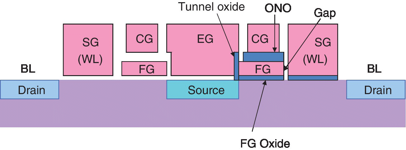
Figure 3.33 Schematic cross‐section of a third generation split gate memory cell showing oxides associated with programming and erase.
Based on V. Markov and A. Kotov (Silicon Storage Technology/Microchip), IEEE Trans. on Devices and Material Reliability, June 2014 [44].
The third generation cell improved program disturb immunity over the previous generation by having a lower source voltage (V s) used for the program operation. This reduced hot carrier effects including the generation of secondary electrons, which are capable of producing program disturb. The high voltage erase operation in this cell was decoupled from the select gate (SG) transistor, which made it compatible with thin gate oxide low voltage CMOS transistors. The scaling of the select gate oxide reduced short channel effects (SCE), which suppressed program disturb induced by subthreshold current.
The effects of single interface traps on program disturb were analyzed. It was found that a split gate memory cell with a high quality Si–SiO2 interface provided the strong program‐disturb immunity that is required for high temperature and automotive embedded applications. Split gate memory cells subjected to 5 × 10⁵ erase/program cycles did not show an acceleration of the program disturb mechanism. Electrons generated by floating gate channel interface traps could not acquire sufficient energy from a low lateral electric field in the channel to surmount the Si‐SiO2 energy barrier.
A reliable 2‐bit/cell vertical split gate embedded Flash memory cell configured for immunity to program disturbs was discussed in July of 2014 by the Chinese Academy of Science and Huahong Grace Semiconductor [45]. A schematic cross‐section of the cell is shown in Figure 3.34. The control gates and floating gates share BL1 and BL2. A chip using this cell architecture was fabricated in 130 nm technology with a 5 F2 bit cell area. A new metal interconnect technique was used for a virtual ground array architecture to improve program disturb as opposed to the conventional AND‐type configuration commonly used. A fully self‐aligned process with shallow trench isolation in the cell array was used to make this word‐line shared split gate structure without having any lithography misalignment issue. A shallow trench isolation (STI) structure was used in the array to relax the lithographic alignment requirement.

Figure 3.34 Schematic cross‐section of vertical 2‐bit/cell split gate embedded Flash memory with shared bit‐lines.
Based on L. Fang et al. (Chinese Academy of Science, Huahong Grace Semiconductor), IEEE Trans. on Electron Devices, July 2014 [45].
A reliability issue, negative charge trapping in the select gate (SG) oxide during a conventional poly‐to‐poly Fowler‐Nordheim tunneling erase operation was found to be an important contributor to the cycling degradation for cells with thin SG oxide. A negative control gate bias erase method was suggested for enhancing the endurance reliability. A 250 °C bake before and after cycling was performed to check the cell data retention characteristics and no extrinsic or intrinsic defects were found. Erase and program characteristics were comparable to conventional split gate cells.
A fully self‐aligned split cell was shown along with a new program disturb immune virtual ground array. A reverse read scheme enlarged the operation window and high endurance reliability was found using a negative voltage‐assisted erase operation. Typical operating conditions used an 8 V program and –7 V erase. For read, the SG was at 4 V. The threshold of one bit is the voltage applied to the corresponding CG terminal to obtain a fixed source‐drain current of 1 μA.
Key blocks of peripheral circuits used for NOR embedded Flash memory were discussed in September of 2014 by the Chinese Academy of Science (CAS), Grace Semiconductor (GSMC), and Shanghai Huahong [46]. These included: a novel source line (SL) voltage compensation circuit and a WL voltage‐generating system. A NOR Flash memory using the two techniques was developed using a GSMC 180 nm 4‐poly 4‐metal CMOS process. The memory used a split gate Flash cell for its fast erase speed, high program efficiency, and large process window. Average standby current for the eFlash array was less than 0.3 μA at 1.8 V and 25 °C. The common source Flash array using the split gate Flash cell are shown in Figure 3.35. The cell is programmed by source‐side channel hot electron injection (CHEI).

Figure 3.35 Common source Flash array with split gate Flash cell.
Based on S. Zhang (Chinese Academy of Sciences (CAS), GSMC, Shanghai Huahong), IEEE Trans. on Circuits and Systems – II. Express Briefs, September 2014 [46].
The new SL voltage compensation circuit controlled the output voltage of the charge pump by considering the number of cells to be programmed with logic “0” data to compensate for the IR drop on the SL decoding path. This stabilized the SL voltage, providing a high program efficiency with low program disturb. To obtain low power consumption in standby as well as high speed in active mode, a WL voltage generating system was developed. A 1.8 V 64 × 32Kbit NOR eFlash was made using the two techniques. The measured standby current at 1.8 V and 25 °C was less than 0.3 μA.
A SPICE macro model of the third generation split gate cell in 55 nm CMOS technology was discussed by CEA‐LETI and Microchip Technology in March of 2015 [47]. A parameter extraction procedure was proposed, which showed good agreement between the model and measurements. The split gate Flash memory was originally developed for low power embedded memory applications in order to improve injection efficiency, erase efficiency, and disturb immunity. It effectively adds a separate access transistor to the Flash memory transistor. The access, or selected gate (SG), transistor controls the current that flows in the memory during read, program, or erase operations. This lowering of the current makes the split gate memories useful in low power applications. Immunity to disturb is improved due to no current flowing when the select gate transistor is opened.
A compact SPICE model connects the process development and the circuit design. The model is intended to accurately reproduce characteristics in the design. For this purpose, model cards with the corresponding electrical characterization extraction parameters are defined. A schematic cross‐section of the 55 nm embedded 2 T split gate Flash memory cell is shown in Figure 3.36.

Figure 3.36 Illustration of schematic cross‐section of 55 nm split gate eFlash cell used for compact SPICE model.
Based on S. Martinie et al. (CEA‐LETI, Microchip Technology), ICMTS, March 2015 [47].
The operating principle is: when the cell is erased, positive charges are stored in the floating gate (FG) and the threshold voltage of the storage transistor is low. When the memory is programmed by the injection of negative charges on to the floating gate, the voltage of the storage transistor becomes higher. The selected gate and storage transistors were modeled using the BSIM3v3 SPICE model. The state is determined by reading the bit‐line current. Biases for erase, program, and read used in the model are shown in Table 3.6.
Table 3.6 Biases for erase, program, and read.
| Operation | WL | BL | SL | EG | CG |
| Erase | 0 | 0 | 0 | Veger | 0 |
| Program | Vwlpg | 0 | Vslpg | Vegpg | Vcgpg |
| Read | Vwlrd | Vblrd | 0 | 0 | Vcgrd |
The macro model of the 55 nm eFlash split gate memory cell was based on a set of equations including main physical aspects of charge and discharge cycles. The model was designed for implementation in SPICE simulators. Good agreement was shown between SPICE simulations and experiments for a range of conditions during operation. This model is currently used in production to optimize 55 nm memory circuits.
A split gate Flash array for automotive and for smart card applications was discussed In May of 2015 by SST/Microchip [48]. This 55 nm logic‐compatible split gate Flash memory, their ESG3 cell, was tested at automotive temperatures and showed fast access and good reliability. It was shown that this Flash memory macro could be embedded in multiple logic process platforms and could be scaled to 40 nm without compromising performance and reliability. A schematic cross‐section of the cell is shown Figure 3.37.

Figure 3.37 Logic compatible split gate Flash cell in 55 nm logic process.
Based on N. Do et al. (Silicon Storage Technology/Microchip Technology), IMW, May 2015 [48].
The cell was scaled from 90 to 55 nm and it was shown that the programmed and erased cell currents remained comparable. A tight distribution of cell current permitted a wide window for operation. It was shown that, with a 4.5 V fixed source‐line voltage, the memory array could sustain up to 12.5 V without any disturb bits after several program cycles. Similarly, with a fixed control gate voltage of 10.5 V, the memory array could sustain up to 6 V without disturbed bits after several program cycles.
A memory array underwent more than 1 million program/erase cycles at 165 °C and remained functional. The automotive specifications used required the Flash macro to have an access time of 10 ns or less and this design provided an access time of less than 7 ns for worst case operation. It was found that the same cell and process could be used to design Flash macros for smart card products that require fast program/erase speeds and high endurance. A 4 Mb Flash macro was shown to require less than 4 ns total time for sector program and erase.
It was found that a smart erase algorithm could be used to enhance endurance performance. A single pulse of erase and program was used to show the intrinsic endurance. At the 55 nm node, this cell array passed qualification at 100 k cycles and 1000 hours of high temperature operating life (HTOL) and data retention storage life (DRSL) bakes in multiple foundries. Efforts were ongoing to scale the cell to less than 0.05 µm2 at the 28 nm node.
In October of 2014, CAS, Shanghai Huahong, and Grace Semiconductor (GSMC) discussed a 1.35 V, 16Mb twin‐bit cell embedded Flash memory with virtual ground architecture [49]. A sensing current protection method was proposed to reduce the sensing margin loss caused by the side‐leakage current in the virtual ground memory array. A reference voltage generating circuit for dynamic sensing window tracking was designed to maximize the sensing window under various process, voltage, and temperature (PVT) conditions. The reference voltage generating circuit and a fast sense amplifier resulted in a high speed read operation. Since four bit‐lines need to be selected to read one bit, a source‐drain‐protection column decoding methodology was used to support the sensing current protection technique.
The eFlash was made in a GSMC 90 nm 4 poly and 4 metal CMOS process. The macro size of the eFlash was 3.2 mm2 and the memory cell size was 0.16 µm2. Access time was 36 nm at 1.35 V. A schematic circuit diagram of the twin‐bit‐cell and a schematic cross‐section are shown in Figure 3.38.

Figure 3.38 Twin bit cell: (a) schematic circuit diagram and (b) schematic cross‐section.
Based on S. Zhang et al. (CAS, Shanghai Huahong, GSMC), IEEE Trans. on Circuits and Systems – I: Regular Papers, October 2014 [49].
The 2‐bits per cell are achieved by treating both the SG and one of the FG devices as transfer gates when accessing the other bit. Due to the symmetrical structure, the CG and S/D terminals must interchange their bias conditions when switching access from Bit1 to Bit2 for both read and program. The cell acts as a conventional split gate cell and uses source side channel hot electron injection (SS CHEI) and poly‐to‐poly FN tunneling erase. A programmed bit has a high V t and stores “0”. An erased bit has a low V t so it stores “1”. Since each FG stores two bits, the twin bit‐cell has four states. The cell size in 90 nm technology is 0.16 µm2. Key performance parameters of the 90 nm 16Mb twin‐bit eNVM include: 36 ns Tac at 1.35 V, 3.8 mA 32 bit read current, 10 µs write time for 8 bits, 1.8 mA active current, and less than 30 μA standby current. Chip size for a 16Mb array was 3.2 mm2.
A 200 KB embedded single 1.5 V power supply EEPROM was discussed in March of 2016 by the Chinese Academy of Science [50]. The device was based on a Shanghai Huahong Grace Semiconductor Manufacturing Corporation (HHGRACE) 90 nm EEPROM process with a 4 poly and 4 metal CMOS [50]. The architecture of the eEEPROM is shown in the block diagram in Figure 3.39.

Figure 3.39 Block diagram of architecture of the embedded EEPROM.
Based on Y. Xu et al. (Chinese Academy of Science), IEEE Trans. on Circuits and Systems – II, March 2016 [50].
Several key design techniques were discussed. An improved bit cell with a larger current sensing window was used in the conventional split‐source EEPROM array. For high speed read a fast sense amplifier and dynamic sensing window tracking reference voltage generating circuit were proposed. The chip size of the EEPROM macro is 1.271 mm2 and the EEPROM cell size is 0.32 µm2. Access time was 30 ns at 1.5 V and 25 °C.
The effect of radiation and stress‐induced degradation on split gate NOR Flash cells was discussed in April of 2016 by NAVSEA Crane [51]. Radiation and program/erase stress on the bit cells was shown to create both positive and negative traps in the oxide around the floating gate. The rate at which oxide traps are neutralized was affected by the annealing temperature following radiation.
3.4.3 Advanced Split Gate Floating Gate Technology below 50 nm
The properties of several embedded nonvolatile memory technologies used in microcontrollers were discussed in May of 2016 by Microchip Technology [52]. These include various types of nitride trapping and floating gate embedded NVM cells as well as several types of emerging NVM technologies.
Being able to scale an embedded technology is important to remain compatible with the CMOS logic it is embedded in. A split gate cell can be made in either charge‐trapping or floating gate technology. Split gate Flash, such as the SG MONOS charge‐trapping technology, has been shown to be scalable from 40 to 28 nm. A cross‐section of the basic split gate SG‐MONOS cell is shown in Figure 3.40 (a) and the split floating gate (SG‐HS3P) cell in Figure 3.40 (b).

Figure 3.40 Cross‐section of (a) basic split gate SG‐MONOS cell and (b) SG‐HS3P floating gate cell.
Based on N. Do (Silicon Storage Technology/Microchip Technology), IMW, May 2016 [52].
The SG‐MONOS is a split gate cell with the nitride charge‐trapping storage under the memory gate and the SG‐HS3P cell uses a floating gate. In the split gate cell, the select gate, or word‐line (WL) gate, can be used to turn off the channel to avoid leakage due to over‐erase.
The ESF3 cells in the bit‐line direction are shown in Figure 3.41. This split gate floating gate cell had the added advantage of a separate erase gate (EG). This cell in 28 nm technology functions up to 170 °C with a cell size of 0.053 µm2. During erase the electrons tunnel between FG and EG with only a positive high voltage bias on the EG polysilicon. This cell can be used in high temperature sub 10 ns access time environments, such as automotive engines. Only the EG is subjected to high voltages. The rest of the device is used at logic voltages and can be scaled with the technology.

Figure 3.41 Schematic cross‐section of ESF3 cell in bit‐line direction.
Based on N. Do et al. (Silicon Storage Technology/Microchip Technology), IMW, May 2016 [52].
In operation for erase, only the erase gate has high voltage applied, with all other inputs at 0 V. For read only logic voltages are applied. For program operation, higher voltages are applied to the CG and the SL. The V t window is greater than 10 V. Program and erase are at 100–500 k cycles.
Optimizing the programming conditions and enhancing the endurance of a third generation SG‐MONOS cell in split gate embedded Flash memory technology was discussed by Microchip in April of 2017 [53]. The new optimization method is based on the use of a two‐step program operation with reduced programming voltage during pre‐programming. This provides a reduction of the peak lateral electric field in the channel at the beginning of the program operation, as a result of a short pre‐programming pulse with reduced V cg1, and resulted in reduced erase performance degradation at the beginning of the program operation. This in turn reduces gate oxide degradation on the hot electron injection area. Additional improvement of endurance and operating performance was attained by reducing the programming time. This was compensated by a slight increase in programming voltage. The faster programming provides lower write energy consumption and higher program‐disturb immunity. Program/erase cycling under this programming condition results in typical endurance of more than 10 million cycles.
A second generation 45 nm split gate embedded Flash that was scaled by 40% to nearly the size of the 28 nm technology node was discussed in May of 2016 by Samsung [54]. No extra masks or processes were used nor was any advanced equipment added to the process. The device had 10 ns random access time, 25 µs write time, and a less than 2 ms erase. Reliability was 1 M cycles of endurance and 20 years data retention, and 1 to 16 Mb capacity macros were verified.
High “on‐cell” current is a key cell parameter for maximizing the endurance cycling limit, which provides fast random access speed. The on‐cell current of a single bit cell is output from three serially connected devices, which are a low voltage word‐line select transistor, a control gate transistor, and a resistor formed in the off‐set oxide spacer region between the WL and the CG. A schematic cross‐section of the cell along with a device schematic showing the resistive effect of the off‐set spacer is shown in Figure 3.42.
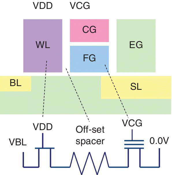
Figure 3.42 Schematic of SG cell and schematic showing resistive effect of off‐set spacer.
Based on Y.K. Lee et al. (Samsung), IMW, May 2016 [54].
For automotive applications, strict quality and reliability is required with zero failure rates at harsh temperature conditions. In May of 2016, Global Foundries and Singapore UT discussed a 16 Mb floating gate (FG) Flash macro in a 2.5 V self‐aligned split gate ESG3 cell in a 40 nm CMOS logic‐compatible process for embedding in automotive microcontrollers [55]. The macro had a dual power supply with operating temperatures from –40 to 150 °C. Random read access was 10 ns under worst case conditions. The technology has a large read current window, which is compatible with both automotive MCU markets and low power modes for smart card and industrial applications.
The cell and erase gate were processed with self‐alignment to the gate spacer. A polysilicon chemical mechanical polishing (CMP) was used that can be integrated into the standard logic process. Code storage requires 1 ns fast random access while data storage requires 200k cycles of endurance and greater than 10 years of data retention. This cell serves both applications. The cell is an ESG3 cell, which is erased using poly‐to‐poly Fowler‐Nordheim tunneling from a field‐enhanced tunneling injector formed between the floating gate and the erase gate. It is programmed using source‐side channel hot electron injection (CHEI). The operating conditions for the 40 nm ESG3 cell are given in Table 3.7. There is a dual 1.1 to 2.5 V power supply. The read IO is 32 bits wide plus 6 bits for error correction.
Table 3.7 Operating conditions for the 40 nm ESG3 cell.
| Erase | Program | Read | |
| Word‐line | 0 V | –1 V | Vdd |
| Bit‐line | 0 V | 1 μA | 0.6–1 V |
| Coupling gate | 0 V | 10.5 V | Vdd |
| Erase gate | 11.5 V | 4.5 V | 0 V |
| Source‐line | 0 V | 4.5 V | 0 V |
A study of program disturb mechanisms in the Microchip/SST ESF3 cell were discussed in May of 2016 [56]. The ESF3 cell is shown in Figure 3.43. Program disturb mechanisms are indicated with numbers.

Figure 3.43 ESG3 cell with program disturb mechanisms shown.
Based on V. Markov et al. (Silicon Storage Technology/Microchip Technology), IMW, May 2016 [56].
The new program disturb mechanisms were identified as: (1) surface generation in the SG transistor with (high E a), (2) interface trap‐assisted BTB tunneling in the gap (low E a), and (3) SG‐oxide trap‐assisted tunneling (low E a). Program disturb mechanisms already identified in earlier generations include: (4) subthreshold current in SG transistor, (5) FG to SG leakage (if isolation defects are present), and (6) secondary impact ionization. A key role was found for certain interface traps located in the cell channel under the select gate (SG) and the split gate gap in acceleration of power dissipation at high and low temperatures.
3.5 Stacked Flash and Processor TSV Integration
An alternative to the embedded Flash memory in a CMOS logic process is integrating an optimized Flash memory with an optimized processor. This can be done using stacked standalone memory chip integration with TSV with the chips side‐by‐side on an interposer chip. An illustration is shown in Figure 3.44 [57].

Figure 3.44 Illustration of stacked chip integration with an interposer with TSV.
3.6 OTP/MTP Embedded Flash Cells and Fuses
A conventional 350 nm CMOS foundry process without extra processing steps was used to fabricate an embedded multiple‐time programmable (MTP) memory array [58]. In June of 2014 researchers from National Chung Hsing University designed this circuit using high‐voltage‐tolerant circuit design techniques to permit the transistors to withstand the higher biases used for program and erasing the NVM cells. A schematic circuit diagram of the MTP cell is shown in Figure 3.45.

Figure 3.45 Schematic circuit diagram of the MTP memory.
Based on C.Y. Huang et al. (NCHU), ISCAS, June 1, 2014 [58].
In addition to the conventional CMOS process, the IP from the high voltage process was used for the program circuitry. Hot hole and hot electron mechanisms were used. This process has a 5 V transistor, which could be run at 8.3 volts for a few programming and erase steps as required in an MTP memory system. By using the high‐voltage‐tolerant design techniques with the current sense amplifiers, random access time reaches 13 ns measured after program. This was thought to be a cost‐effective method for designing the high voltage parts of the eFlash chips.
Read and write capability for a one transistor one‐time‐programmable (OTP) anti‐fuse cell macro was made in a TSMC 16 nm CMOS FinFET process in September of 2014 by Sidense [59]. These OTP macros had been used for designs from 180 nm to 28 nm technology and have been proven in 20 nm technology. Early test results confirmed correct bit‐cell operation on a 16 nm FinFET device with a program voltage comparable to the 1 T OTP device in 28 nm technology, but with 10 times lower leakage current. Programmed characteristics were as good as those for 20 nm cells with large margins between programmed and unprogrammed cells. Post‐bake bit‐cell stability was also good. The 16 nm macro was indicated as a potential option for design into devices for mobile circuits.
A logic process compatible OTP memory in Hi‐K metal gate (HKMG) CMOS was made in December of 2015 by NCTU and UMC using a new dielectric fuse breakdown mechanism [60]. The breakdown observed in HKMG CMOS technology was found to be different from conventional anti‐fuse dielectric breakdown. It showed a property of an open gate and could be operated at a program current of less than 50 μA and speed of 20 µs, which is an improvement over conventional fuse mechanisms. Cross‐sections of 28 nm MOSFETs made to investigate the dielectric fuse mechanism are shown in Figure 3.46. Figure 3.46 (a) shows an SiO2 polysilicon nMOSFET and Figure 3.46 (b) shows an HfON HKMG nMOSFET.

Figure 3.46 Schematic cross‐sections of (a) 28 nm SiO2 poly‐silicon nMOSFET gate and (b) HfO2 HKMG nMOSFET gate.
Based on E.R. Hsieh et al. (NCTU, UMC), IEDM, December 2015 [60].
For IoT applications there is demand for reliable OTP functionality at low cost. Figure 3.47 shows the characteristics of a gate current for a conventional gate dielectric anti‐fuse and the HKMG dielectric fuse mechanism discussed here.

Figure 3.47 Characteristics of gate current for gate dielectric anti‐fuse and HKMG dielectric fuse.
(Based on E.R. Hsieh et al. (NCTU, UMC), IEDM, December 2015 [60]
The conventional antifuse breakdown causes a sudden increase to a high gate current; however, the new mechanism has the current suddenly shut off and the gate open. After anti‐fusing, the gate current increases rapidly and after fusing it is blocked.
An embedded logic‐compatible multiple time programmable NVM element was discussed in January of 2017 by IBM and UCLA [61]. The memory was intended for use in high‐k metal gate (HKMG) CMOS technologies such as SOI and FinFET, which exhibit self‐heating.
The memory device exploited an intrinsic device self‐heating enhanced charge trapping in logic devices made in CMOS HKMG technology. A unique multiple time programmable embedded NVM element was developed, which was called a charge trap transistor (CTT). The intrinsic self‐heating charge trapping memory is applicable to use in SOI and in bulk FinFET technology since self‐heating occurs in bulk FinFETs although less than in SOI FinFETs.
Functionality was shown for fully functional memory arrays at 22 nm planar and 14 nm FinFET technology nodes. The density for 22 nm was 0.144 µm2 per bit and for 14 nm FinFET technology was 0.082 µm2/bit. The devices were logic voltage compatible. Peak power operation was about 4 mW and good data retention was shown for a fully integrated and scalable embedded NVM without adding process complexity or mask layers.
The HfO2‐based HKMG devices were developed as nonvolatile memory elements for SoC applications in HKMG CMOS technologies. Intrinsic self‐heating in enhanced charge trapping HKMG devices was used to achieve large and stable device threshold voltage shifts suitable for memory applications. Multiple time programming was shown to be possible.
A new embedded Flash memory with a reversed drain‐source cell was discussed in May of 2017 by SMIC [62]. The mechanism was intended to improve the read stress and the standby with power‐on after more than 20 program/erase cycles, which causes conventional embedded Flash memory to fail read “0”. A schematic cross‐section of the cell biased for the read operation is shown in Figure 3.48 for (a) the conventional eFlash cell and (b) the new reversed eFlash cell.

Figure 3.48 Schematic cross‐section showing read operation of (a) conventional eFlash cell with location of high field stress on the tunnel oxide indicated by the dot and (b) reversed eFlash cell with reduced stress on the tunnel oxide.
Based on L. Shao et al. (SMIC), CSTIC, May 2017 [62].
The stress‐induced leakage current (SILC) mechanism of an eFlash with a conventional e‐Flash cell is caused by the high electric field stress on the tunneling oxide of the device at the source side during read, which causes traps formed during programming and erase to leak current. In the reversed eFlash cell, the low voltage on the drain during read reduces this leakage. The result is less SILC leakage for a multiple time programmable device.
3.7 Stacked Gate Double Poly Flash
Embedded Flash memory was made on a 55 nm deep depleted channel (DDC) platform with ultralow power of <0.9 V by Fujitsu in December of 2013 [63]. While the DDC process has a reduced thermal budget, the single bit charge loss of Flash after cycling can be optimized so it is comparable to baseline eFlash. It was verified that improved variability and low power digital performance of the DDC process was maintained in the embedded Flash flow. The DDC transistor has also been found to achieve ultralow voltage SRAM operation and to improve digital and analog performance by reduction in random dopant fluctuation.
Having an embedded NVM available in this process was expected to enable a wide range of ultralow power applications such as smart cards, energy harvesting, and sensor MCU for Internet of Things applications. A cross‐section of the DDC transistor is shown in Figure 3.49. The DDC transistor has an undoped epitaxial layer and a V t setting layer. The DDC process uses a reduced thermal budget to suppress impurity diffusion into the undoped epitaxial channel layer.

Figure 3.49 Schematic cross‐section of DDC transistor showing undoped epitaxial layer and Vt setting layer
Based on M. Hori et al. (Fujitsu), IEDM, December 2013 [63].
The memory cell layout of the 1 T NOR FLOTOX Flash macro used contains 512 word‐lines and 1024 bit‐lines, resulting in 512K cells. The memory transistor is made by adding processing to a DDC transistor. Steps in the DDC process are modified for the embedded Flash. The undoped epitaxial layer is thickened to compensate for silicon loss during the additional oxidation steps for Flash tunnel oxide and high voltage gate oxide. Temperatures for Flash‐related steps are lowered significantly to suppress impurity diffusion from the screen layer to the undoped epi channel layer of DDC transistors. Channel and drain for Flash and HV transistors are modified.
An embedded stacked floating gate Flash cell embedded in 65 nm logic technology was discussed in September of 2012 by Lattice Semiconductor and Fujitsu [64]. The logic transistor characteristics were optimized for low standby current for use in consumer applications. This cell was scaled from an older 90 nm stacked Flash cell technology. The gate length and active width are both 200 nm. The cell size is 0.253 µm2, which represents a 42.6% cell area reduction compared with the 90 nm cell. It also showed an 8.6% reduction in programming voltage compared with the previous 90 nm cell. The gate‐induceddrain leakage (GIDL) current was reduced by about an order of magnitude. Typical operating conditions of the Flash cell included an 8.5 V program and a 17 V erase composed of –8.5 V on the gate and 8.5 V on the well. Read was at V drain of 0.45 V with V source grounded and gate at 4.65 V.
Reliability requirements of the automotive industry for electronic components are challenging. In April of 2013, the University de Studi di Ferrara and Infineon discussed automotive reliability requirements for Flash memories [65]. Erratic bits are considered a major reliability issue conventionally handled by repair strategies ranging from static redundancy to dynamic correction codes. Both repair strategies need to be tailored to the product.
A signature classification methodology for erratic bits was suggested that helps choose the best repair strategy for each bit. This tends to reduce using unnecessary correction techniques and increase the chip error probability by improving the accuracy in modeling. The classification methodology is to be performed either during a wafer sort or in confidence level testing for product monitoring. It is based on the analysis of the features constituting the bit signature. This classification permits speculation of the most efficient repair strategy for each erratic signature class. It is expected that this will reduce the redundancy usage. Models were developed as a validation of the proposed approach.
The challenges of integrating a conventional nonvolatile double polysilicon NVM memory array in a base‐line CMOS process were discussed by On Semiconductor in May of 2015 [66]. Process modules of ONO and floating poly were studied. The addition of new implant steps such as deep wells and high voltage LDD were discussed along with new critical etch steps such as removal of sacrificial oxide in the NVM, high voltage and low voltage ONO etch, and stack poly etch. New layers also need to be added, such as tunnel oxide, floating gate poly, and ONO. A schematic process flow for an embedded NVM integration in base‐line CMOS is shown in Figure 3.50.

Figure 3.50 Schematic process flow for an embedded NVM in base‐line CMOS. Bullets in dashed boxes are part of the conventional CMOS process. Bullets in double outlined boxes are added depositions and italicized bullets are added etches.
Based on M. Agam et al. (On Semi.), ASMC, May 2015 [66].
The basic criteria for process flow integration is that base‐line process steps should not change and that any added process steps have minimal impact. While the NVM technology with floating poly had many integration issues that were addressed, the constraints of the ONO layer were found to be particularly challenging. High voltage transistors were also carefully considered.
An embedded Flash cell made on 300 mm wafers in 130 nm bipolar, CMOS, and DMOS (BCD) technology (5 to 80 V) was discussed in June of 2014 by Rohm and Genusion [67]. The eFlash cell had data retention of greater than 20 years under 150 °C testing after 100k erase/write cycles. BCD (bipolar, CMOS, DMOS) is a key technology for power ICs. BCD devices are widely used in automotive and industrial applications to improve performance and intelligence. The BCD platform permits the flexibility to choose various types and performance of devices. The reliability of BCD devices under high temperature is an important factor.
The 130 nm Rohm BCD platform is shown in Figure 3.51. The 1.5/5.5 V CMOS and IP core are standard to the platform. Device options include: DMOS, HV CMOS, power CMOS, bipolar, MIM/MOM capacitors, poly‐Si resistor, Flash cell, DTI, SRAM, and OTP. There are three modules of wiring options that can be combined with the standard platform as desired.

Figure 3.51 A block diagram of the 130 nm platform in bipolar, CMOS, and DMOS (BCD) is shown.
Based on K. Iwamoto et al. (Rohm, Genusion), International Symposium on Power Semiconductor Devices and ICs, June 15, 2014 [67].
An embedded NOR Flash memory cell was developed for the 130 nm BCD platform. The cell used a back‐bias assisted band‐to‐band tunneling mechanism. The unit cell size was 0.267 µm2.
The B4 Flash cell adopts the standard floating gate type structure, which fits well with both the CMOS and BCD processes. A top‐down schematic view of the layout of the embedded NOR Flash memory cell is shown in Figure 3.52.

Figure 3.52 Top‐down schematic view of layout of eNOR Flash cell.
Based on K. Iwamoto et al. (Rohm, Genusion), International Symposium on Power Semiconductor Devices and ICs, June 15, 2014 [67].
The two companies jointly developed the 90 nm B4‐Flash NOR memory and have it currently in production. The drain profile is optimized to maintain its intrinsic characteristics even in the BCD process. The V th distribution at 150 °C after 100 K P/E cycles was demonstrated and also a 1.5Kbit cell array, which was extrapolated to the 288Kbit production array. The V th window had a good margin after 100 K P/E cycles. The chip showed good reliability under high temperature ambient. The eFlash memory cell was successfully integrated into the 130 nm BCD platform.
3.8 Charge Trapping eFlash
3.8.1 Overview of Early Embedded Charge Trapping Memory
Embedded charge trapping memories are in production at several manufacturers and the technology is also widely expected to be used in standalone vertical memories. Production examples are discussed in the first section followed by technology development in the second.
Cypress, Renesas, and Spansion, now owned by Cypress, are in production with charge trapping NV memory. Cypress is working with Foundries Shanghai Huali and UMC to produce its 55 nm SONOS technology for smart cards and IoT. UMC is already in production with the Cypress 65 nm charge trapping technology. Renesas has produced embedded split gate MONOS Flash macros for MCU for various microcontroller applications since 2004 and are currently in production in 40 nm technology. Spansion had charge trapping Flash memory devices in production from the 110 nm to 65 nm technology nodes in December of 2014.
In June of 2003, Halo LSI discussed a 180 nm twin MONOS NOR‐type Flash memory that used a simple process making it suitable for embedded Flash applications [68]. A 128KB device with a 4 ns access time was discussed. The twin MONOS technology had low voltage operation and a simple process. The maximum high voltage requirement was limited to 4.5 V. Only three extra masking steps were required even though the cell size was around 5–7 F2, which permitted larger memory macro sizes to be integrated on a logic chip. An implementation for an embedded program and data storage required access times between 10 and 20 ns. A schematic of the twin MONOS cells cross‐section is shown in Figure 3.53.

Figure 3.53 Schematic cross‐section of twin MONOS cells.
Based on T. Ogura et al. (Halo LSI), VLSI Circuits Symposium, June 2003 [68].
The cell consisted of a word gate, two side wall control gates, and two diffusion regions. A thin gate oxide was used beneath the word gate. An ONO film was used beneath the side wall control gates. No charge pump was required during read. For the memory array, the read voltage was 1.8 V with I on >60 μA/µm and I off of 3.5 μA/µm. Read access time was 20 ns. Program was at 5.5 V on the control gate and program current was <2 μA/bit for 20 µs. Erase by HHI was 4.5 V on the BL with an erase current of 2 nA/bit.
A 512KB MONOS Flash memory module made in a 180 nm CMOS logic process and intended for embedding in a microcontroller was described by Hitachi in June of 2003 [69]. The read path of the module was composed of the same low voltage transistors that were used in the CPU core. This provided a compact layout of the peripheral circuits. Read access was 34 MHz. For a 64KB block, program time was less than 4 ms and erase time was less than 11 ms. The module area was 5.4 mm2. I ds was 20 μA at V cg = 1.5 V.
A local SONOS structure for an embedded NVM cell in 130 nm standard CMOS logic was discussed by Samsung in June of 2003 [70]. A localized silicon nitride storage layer gives a complete erase, low program current and high on‐cell current from a low threshold voltage. The split gate local SONOS cell is shown in Figure 3.54, where (a) illustrates a top‐down view of the layout showing the localized ONO structure and (b) illustrates a schematic cross‐section of the cell with the halo implant junction engineering shown.

Figure 3.54 Split gate local SONOS cell in conventional CMOS logic: (a) top‐down view showing localized ONO layer and (b) schematic cross‐section showing Halo implant junction engineering on the source side.
Based on J.H. Kim et al. (Samsung), VLSI Technology Symposium, June 2003 [70].
This 0.276 µm2 local SONOS NVM cell had a 20 µs program and 2 ms erase speed using 5.5 V bias. Three added masks were required to make the SONOS cell and four more were required for the high voltage operation. This is four masks less than an embedded floating gate NVM. The local SONOS showed more complete erase characteristics than a longer SONOS layer. A halo implantation was used to suppress the drain depletion region punch‐through and improve program/erase efficiency. The localized ONO and junction engineering permitted low voltage operation, where 4.5 V on the word‐line resulted in sufficient threshold voltage shift. Program current was as low as 10 μA/cell. Program speed was 20 µs and erase speed was 2 ms.
An 8Mbit macro of split gate localized SONOS charge trapping memory in a 130 nm conventional logic process with five‐level copper metallization was shown by Samsung in June of 2004 [71]. Cell size was 0.276 µm2. Read speed was up to 60 MHZ at V cc = 0.9 V and 85 °C. Current consumption was less than 5 mA at V cc –1.4 V. The cell was programmed by channel hot electron injection (CHEI) and erased by hot hole injection (HHI). The localized ONO storage technology of this cell was found to have better endurance and higher immunity to read disturb than conventional stacked SONOS due to its limited ONO layer and asymmetrical cell structure. After 100 k P/E cycles the sensing current margin is maintained due to its localized ONO layer.
This 256 K × 32 SONOS embedded Flash EEPROM macro in a 130 nm CMOS logic compatible process was discussed further by Samsung in June of 2004 [72]. Cell size was 0.276 µm2. Program time was 20 µs and erase time was 20 ms. A new address transition detection (ATD) assisted current sense amplifier was used for the low V cc application, where V cc was –0.7 to 1.4 V. The read operation was done at 66 MHz with a low active current of 5 mA being typical.
In June of 2006, Genusion described a p‐channel SONOS Flash memory cell technology with good scalability and high programming efficiency for NOR architectures [73]. The cell used a back bias assisted band‐to‐band tunneling induced hot‐electron (B4‐HE) injection process. If a moderate back bias is applied to the cell during programming, the bit‐line voltage can be reduced below the supply voltage, which is 1.8 V. The gate length is 60 nm. Operation of the 50 nm B4‐Flash cell was confirmed. The programming method provided low drain voltage programmability below 1.8 V and high program efficiency.
The back bias assisted BTBT‐HE generation consists of two steps. The first is BTBT generation and the second is electron acceleration. A schematic cross‐section showing the location of the BTBT generation and electron acceleration is shown in Figure 3.55.

Figure 3.55 Illustration of location of BTBT generation and electron acceleration in SONOS cell.
Based on S. Shukuri et al. (Genusion, Tohoku University), VLSI Technology Symposium, June 2006 [73].
Program has the V g at 12 V with V b = 4.2 V and erase has V g at –12 V. Read is V g = –2 V with V d = 1.8 V. In embedded applications, the high program efficiency may help achieve high area efficiency due to reduction of the on‐chip power supply capability. Erase time was about 100 ms by FN tunneling hole injection. Data retention of 10 k cycled cells at the maximum temperature is 10 years at around 125 °C.
3.8.2 Embedded 40 nm Charge Trapping (MONOS) Flash MCU
In May of 2012 an embedded Flash‐based MCU platform was announced based on the Renesas 40 nm MONOS eFlash technology, which was expected to be licensable to other semiconductor suppliers [74]. The platform integrated the 40 nm MONOS eFlash technology and TSMC CMOS logic and analog IP. Details of the arrangement were still being discussed. The Renesas 40 nm Flash had 20 year data retention and could be read up to a 170 °C junction temperature. The code Flash supported read speed of 120 MHZ with 20 year data retention after 125 000 program/erase cycles.
Flash MCUs with embedded Flash memory are considered essential in automotive applications for complicated real‐time controls for higher fuel‐efficiency, better safety and increased connectivity. High density, fast random read access is needed from the eFlash. The requirements for eFlash in automotive products are secured operations and data reliability in particular reliable program/erase cycling at high temperature.
In January of 2014, Renesas discussed its 40 nm embedded split gate (SG) MONOS Flash macros for the automotive market [75]. These devices had 160 MHz random access for code. They had endurance over 10 M cycles for data at a junction temperature of 170 °C. A sense amplifier with digital offset cancellation had a fast read operation greater than 160 MHZ. Program time was decreased by an adaptable program current control method and an intelligent erase method decreased the erase time. 3D stacked capacitors provided an area‐efficient charge pump. Both a 2 MB code macro and a 64KB data macro were fabricated in a 40 nm eFlash process. The code macro had 160 MHz random read at Tj = 170 °C. A 5.1 GB/s read throughput was reached by a simultaneous 256 bit read‐out from two code macros. The data macro had P/E endurance over 10 million cycles at T j = 170 °C without any software‐assisted techniques.
The trend of eFlash memories in high‐end Flash MCUs is to have both a code macro and a data macro. The code macro is used to store the boot/application codes. These codes require large capacity and fast read at wide temperature ranges. The data macro, however, is a substitute for external EEPROM to reduce system cost. Its contents are frequently rewritten after shipment. The data macro must meet a high program/erase endurance over a wide temperature range.
Flash MCUs with embedded Flash memory are used in automotive applications for complicated real‐time controls for higher fuel efficiency, better safety and increased connectivity. Both high density and fast random read access are needed from the eFlash. The requirements for eFlash in automotive products are secured operations and data reliability including reliable program/erase cycling at high temperature.
In February of 2013, Renesas discussed a 40 nm eFlash macro for automotive applications [76]. It had three key features: a 40 nm scaled split gate (SG)‐MONOS cell, an over 160 MHz random read access with appropriate sense amplifier, and circuit techniques for fast reliable P/E at a junction temperature of 170 °C. The architecture of the split gate MONOS cell is shown in the schematic cross‐section of the SG‐MONOS device in Figure 3.56 (a). Operational voltages are shown in Figure 3.56 (b). There is no high voltage applied during program or erase on the WL and BL side of the circuit. The high voltage during P/E is applied only to the separate memory gate (MG) and SL nodes. The WL and BL side of the circuit are used during read and only CMOS logic voltages (V dd) are applied to the WL and BL side.

Figure 3.56 SG‐MONOS eFlash cell: (a) cell architecture and (b) operational voltage.
Based on T. Kono et al. (Renesas), IEEE ISSCC, February 2013 [76).
The SG‐MONOS cell uses a split gate cell with charge‐trapping storage in a nitride film. The cell has two advantages over a conventional one transistor cell. The word‐line voltage in the read operation is at the logic power supply voltage because there is no column current leakage with the thin split gate oxide. Fast read paths can be built with fast low voltage transistors because high voltage for P/E are not applied to them. Fast programming with small cell current around 1 μA can be realized because of the source‐side injection capability. For the erase operation, hot hole injection by band‐to‐band tunneling is used, which has a high erase speed that enables a short erase time with a small erase unit.
For P/E operations at 170 °C, two circuit techniques were used [76]. An adaptable program current control method was used with two data latches per main BL. One stores the program data from the Flash controller and the other stores the verification result for the SA. These data and output from the fail bit counter control the program current. An intelligent erase method was used. A simulation with a 40 nm SG‐MONOS cell showed a 60% decrease in total erase pulse time. By using poly‐insulator‐poly (PIP) capacitors and a metal‐oxide‐metal (MOM) capacitor stacked over the 5 V MOS capacitors, a unit capacitor with small area and high breakdown voltage was confirmed and the area of the VSP charge pump decreased by 44%.
In the eFlash macro with the SG‐MONOS cells, the eFlash was used in both the data memory and the code macro. These circuit techniques were used to develop a 2 MB code macro and a 64 KB data macro in a 40 nm eFlash process. The read frequency of the code macro was confirmed at >160 MHz at 170 °C. By reading 256 bits from two code macros simultaneously, the maximum read throughput reached 5.1GB/s. The data macro achieved the P/E endurance over 10 M cycles at 170 °C without wear‐leveling.
In April of 2015, Renesas and Hitachi discussed the data retention mechanism of an embedded split gate MONOS Flash memory [77]. A data retention model was developed based on the thermionic emissions and a simple estimation method with a long lifetime and wide temperature range. A process flow for the embedded MONOS Flash was developed, which included: well/ channel implant, CG‐oxidation, CG‐poly etch, MG channel implant, SiO2/SiN/SiO2 deposition, MG‐poly deposition, Mg‐ poly etch, removal of SiO2/SiN/SiO2, extension and pocket implant, side wall formation, and source/drain diffusion implant.
The retention results for the embedded SG‐MONOS Flash were consistent with previous results within a temperature range of 150–450 °C. The MONOS memory with split gate had a 20 year lifetime at more than 200 °C. This SG‐MONOS memory is for use in an MCU in 150, 90, and 40 nm process generations. It withstands operating temperatures higher than 170 °C and has better than 20 year data retention in automotive MCU. Operating condition voltages are shown in the schematic cross‐sections of the SG‐MONOS cell in Figure 3.57 for (a) program, (b) erase, and (c) read.
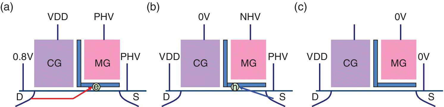
Figure 3.57 Schematic cross‐section of the SG‐MONOS cell with operating condition voltages for (a) program, (b) erase, and (c) read.
Based on Y. Kawashima et al. (Renesas, Hitachi), IRPS, April 2015 [77].
A data retention model and estimation method based on thermionic emissions was developed. This method can measure the trap density of nitride rapidly. The data retention lifetime could be estimated over a time and a wide temperature range. The SG‐MONOS device was found capable of a 20 year lifetime at more than 200 °C.
3.8.3 Embedded 28 nm Charge Trapping (MONOS) Flash MCU
The development of a 28 nm eFlash MONOS technology for MCU was announced by Renesas in February of 2014 [78]. A primary target application for the technology was automotive control systems. The earlier 40 nm production technology supported up to 8 MB of on‐chip Flash memory for MCU while the 28 nm technology was expected to support 16 MB of macro density. The 28 nm prototype chip could support clock frequency of 160 MHZ, data retention time of 20 years, and 250 000 cycles of endurance.
The 28 nm embedded split gate SG‐MONOS Flash memory macro for automotive applications was also discussed by Renesas in April of 2014 [77]. This device had a 200 MHz read and 2.0 MB/s write throughput at a junction temperature (T j) of 170 °C. The split gate‐MONOS cell had high voltage only on the memory gate for programming and erase with only logic voltage on the select gate, as shown in the schematic cross‐section of the cell in Figure 3.58.
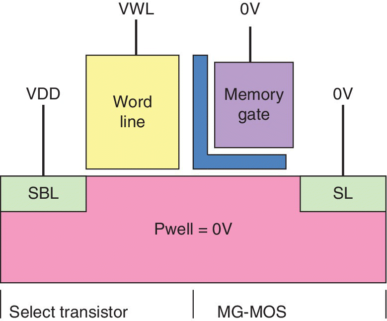
Figure 3.58 Split gate MONOS cell showing high voltage only on memory gate for P/E.
Based on Y. Kawashima et al. (Renesas, Hitachi), IRPS, April 2015 [77].
The transistors and interconnections used in embedded Flash systems tend to effect reliability in the sub 40 nm technology generations. Thin transistor oxide films can degrade the time‐dependent dielectric breakdown (TDDB) lifetime. The SG‐MONOS device had a temperature adjusted overdrive word‐line voltage control, which permitted both 200 MHZ random access and greater than 10 times longer TDDB lifetime for the word‐line drivers. It also had a high voltage control technique to relax electrical stress on memory cells and peripheral devices by using temperature adaptive step pulse erase control. Write throughput of 2.0 MB/s was achieved by source‐side injection programming with a negative back‐bias, which permitted a 63% reduction of program pulse time. RF noise was reduced by 19 dB using a spread spectrum phase shifted clock generation technique. The eFlash architecture included two code Flash macros and a data Flash macro, both made up of SG‐MONOS cells each using a split gate charge trapping cell. The memory cell size was 0.053 µm2.
The 28 nm split gate embedded MONOS was discussed by Renesas in June of 2015 for use in MCUs for vehicle control systems such as power train, chassis, and brake control [79]. Powertrain applications, in particular, require a large memory capacity as well as having a 170 °C temperature rating. The application requires speed and split gate cells tend to be fast and have a low power read due to the low voltage swing of the word‐line. The charge trapping structure leads to high data reliability due to robustness against point defects and the low cell profile assures better compatibility with the CMOS logic process than a floating gate. The 28 nm SG‐MONOS macro had 200 MHz random read for code Flash and over 1 M program and erase cycles for data Flash. An 80% smaller sleep current was achieved at a junction temperature of 170 °C by using a floating bit‐line and raised V SS with a lowered V DD for the memory cell.
In January of 2016, Renesas discussed a 28 nm embedded split gate MONOS Flash memory macro intended for automotive applications [80,81]. This device had a 6.4GB read throughput using a 200 MHz no‐wait read operation and a 2.0 MB/s write throughput at a junction temperature (T j) of 170 °C. These 28 nm eMONOS Flash macros were developed to increase memory capacity embedded in scaled microcontroller units and also to improve performance over a range of junction temperatures from –40 to +170 °C, which are the automotive under‐the‐hood specifications.
An issue of scaling the process is the resulting degradation of reliability characteristics. In this study, a temperature adjusted word‐line overdrive method was used to improve random read access frequency by 15%, as well as have 6.4GB/s of read throughput for 200 MHz no‐wait random access for code Flash macros. TDDB lifetime of WL drivers was increased by 10 times. Temperature adaptive step pulse erase control (TASPEC) was used to improve the TDDB lifetime of dielectric films between metal interconnect layers by 3 times. TASPEC was used for a data Flash macro with 1 × 10⁶ rewrite cycles. Programming by source side injection (SSI) using negative back‐bias voltage achieved 63% reduction of program pulse time and resulted in 2.0 MB/s write throughput of code Flash macros. A spread spectrum clock generation and a clock phase shift technique were developed for charge pump clock generation to suppress EMI noise due to high write throughput of the code Flash macros and reduce peak power of EMI noise by 19 dB.
An SG‐MONOS cell was used that combines a split gate cell and a discrete charge trapping cell. Split gate cells have a fast random read access speed since the read path can consist only of logic CMOS transistors. Fast program speed is due to the efficiency of source‐side injection (SSI). Erase operation uses hot hole injection by band‐to‐band tunneling (BTBT) and is faster than Fowler‐Nordheim (FN) tunneling. The schematic cross‐section of the MG‐SONOS cell in Figure 3.59 illustrates SSI programming and BTBT erase. Figure 3.59 (a) illustrates SSI programming with the memory gate (MG) at positive high voltage (PHV) and the WL and BL at appropriate logic levels. Figure 3.59 (b) illustrates band‐to‐band tunneling (BTBT) erase with negative high voltage (NHV) on the memory gate while the BL and WL remain at appropriate logic levels.

Figure 3.59 Cross‐section of MG‐SONOS cell showing (a) SSI program and (b) BTBT erase.
Based on Y. Taito et al. (Renesas), IEEE Journal of Solid‐State Circuits, January 2016 [81].
The memory cell height of the floating gate type of cell is twice the height of logic CMOS transistors in the 28 nm process whereas the height of the SG‐MONOS cell is closer to that of the CMOS logic transistors. A high‐k metal gate process is used, which makes it is necessary for the Flash memory cells to be polished to the same height as the logic CMOS transistors by chemical mechanical polishing (CMP). This is easier in the lower height MONOS process than in the double poly floating gate process.
In the 28 nm eFlash SG‐MONOS system, the memory block contains two types of eFLash macro. Code Flash is used to store control program code and requires fast random read access and large memory capacity. The code Flash does random read at a frequency of 200 MHz. Program speed is 2.0 MB/s and erase speed in 0.91 MB/s. Its maximum capacity is 32 MB. The P/E endurance requirement is 10 k cycles. The performance of the code Flash random read access frequency is increased by 15% using a temperature‐adjusted WL overdrive scheme. Write pulse time is reduced by 63% using an SSI program and negative back‐bias voltage.
The data Flash is used for data storage and requires good rewrite endurance and small rewrite unit size. Rewrite endurance of the data Flash macro is 1 × 10⁶ cycles. An SSCG and a clock phase shift technique are used to solve the EMI noise caused by charge pump operation during field programming. The rewrite unit size is 64KB while the maximum capacity is 512MB. The cell size of the 28 nm SG‐MONOS is 0.053 µm2, core power supply is 1.1 V, and IO supply range is 2.7 to 5.5 V. The operating temperature ranged from –40 to +170 °C.
3.8.4 Embedded Application‐Specific 1T‐MONOS Flash Macro
The computerization of automotive control has expanded the application range of MCUs. In February of 2016, Renesas discussed a 90 nm one transistor (1T) MONOS eFlash macro for use in high end automotive applications such as a high end engine control unit (ECU) [82]. A schematic cross‐section of the 1T cell is shown in Figure 3.60.

Figure 3.60 Schematic cross‐section of 90 nm 1T MONOS eFlash Cell.
Based on H. Mitani et al. (Renesas), ISSCC, February 2016 [82].
This memory cell used Fowler‐Nordheim tunneling for both program and erase operations. The cell had a read‐disturb‐free array architecture to ensure automotive grade reliability. It achieved over 100M cycles of rewrite endurance at 175 °C junction temperature (T j) by using an adaptable slope pulse control technique. As a result total power consumption was reduced to 0.07 mJ/8KB using a 98 μA program erase current. A low power system control method using the 1 T‐MONOS device resulted in a 99% power reduction. A block diagram of a Flash MCU with the 1 T‐MONOS integrated for a low power system is shown in Figure 3.61.

Figure 3.61 Block diagram of low power Flash MCU with 1T‐MONOS aacro.
Based on H. Mitani et al. (Renesas), ISSCC, February 2016 [82].
The 1T MONOS memory device was made in a three‐layer aluminum process. Memory capacity of the macro was 128KB and it used a 3.3 V power supply. The operating temperature range was –40 to +175 °C. Read I/O has 32 bits + <run on text > 7 bits. The random read frequency was greater than 50 MHz. Program time was 3 ms per 128 B and erase time was 5 ms per 2KB. Program and erase current was 98 μA.
In February of 2016, Renesas announced the development of a 90 nm one‐transistor (1 T) MONOS [83], which could be integrated with various processes including CMOS, bipolar CMOS, and DMOS. It provided a high program/erase endurance of over 100 million cycles with a junction temperature (T j) of 175 °C and a low rewrite energy consumption of 0.07 mJ/8KB. The 128KB Flash memory prototypes were shown with a low rewrite current of 98 μA. It is expected that this technology can be added to automotive analog devices to improve performance and reliability.
3.8.5 FinFET SG‐MONOS
For a future automotive MCU with embedded memory, in December of 2016, Renesas and Hitachi discussed a FinFET split gate MONOS embedded Flash memory in 16/14 nm technology node [84]. The subthreshold characteristics and small threshold voltage variability due to the FIN were explored. The FIN top‐corner effects were found to be well suppressed by incremental step pulse programming for source side injection. Data retention at 150 °C after 250k program/erase cycles was confirmed for use in advanced automotive system applications.
In December of 2016 Renesas discussed embedded Flash technology for automotive applications such as higher fuel efficient engines and advanced driver assistance systems (ADAS) [85]. The attributes of a charge trapping split gate type of data storage such as SG‐MONOS were given. Split gate cells permit fast speed and low power read due to the low voltage swing of the word line. The charge trapping structure is robust against point defects, which could cause a floating gate to lose all stored charge. Charge trapping technologies also have a lower cell height, making them more compatible with the CMOS logic process. A 28 nm SG‐MONOS is targeting over 160 MHz of random read. 1M program/erase cycles have been found for data Flash at a junction temperature of 170 °C. Temperature adaptive step pulse erase control improves the TDDB lifetime of dielectric films between metal interconnect layers by three times to improve endurance characteristics of SG‐MONOS.
A 1.5 transistor SG‐MONOS cell using a Fin structure was discussed along with its advantages over a one transistor cell. Bulk FinFET SG‐MONOS Flash was shown. Cell characteristics using source‐side injection (SSI) programming and erase using band‐to‐band tunneling (BTBT‐HHI) were compared to that of the planar structure. Incremental step pulse SSI techniques were confirmed for suppression of Fin top‐corner effects.
A schematic process flow for the integration of the SG‐MONOS device into the FinFET is shown in Figure 3.62. The Fin is formed first on the bulk silicon wafer by patterning the active area and recessing the STI oxide. This is followed by the SG‐MONOS process, which follows nearly the same sequence as conventional planar FG‐MONOS. The FinFET SG‐MONOS is very compatible with the process of the logic transistors.

Figure 3.62 Schematic process flow of formation of the fin of the FinFET and the SG‐MONOS.
Based on S. Tsuda et al. (Renesas Electronics, Hitachi), IEEE IEDM, December 2016 [84].
The control gate (CG) and memory gate (MG) lengths of the FinFET SG‐MONOS are equivalent to the planar device. Due to the fully depleted state, the subthreshold swing of the FinFET SG‐MONOS is smaller than that of the planar SG‐MONOS and the threshold voltage distribution is improved. The on‐current of the FinFET SG‐MONOS is comparable to the planar SG‐MONOS even though the footprint of the Fin is 20% of the planar. The FinFET SG‐MONOS shows a steeper subthreshold swing than the planar SG‐MONOS whether the devices are programmed or erased. This improved the current controllability results in a larger current window for the FinFET SG‐MONOS. Program and erase time are 100 µs. A 3D schematic showing the integration of the FinFET SG‐MONOS and the logic FinFET CMOS is shown Figure 3.63. The two structures are the same height.

Figure 3.63 Schematic of integration of FinFET SG‐MONOS and logic FinFET CMOS.
Based on S. Tsuda et al. (Renesas Electronics, Hitachi), IEEE IEDM, December 2016 [84] (permission of IEEE).
The improved subthreshold characteristics and small threshold voltage variability due to the Fin structure are required for future low power operation. The cell current window is wider than the conventional planar SG‐MONOS. Incremental step pulse programming for source side injection was effective in suppressing the Fin top corner effect. Data retention at 150 °C after 250k program/erase cycles indicates sufficient reliability for advanced automotive applications. The Fin technology permits scaling to the 16/14 nm node. The low profile of the SG‐MONOS permits integration with FinFET logic CMOS with a high‐k metal gate made by a gate last process.
3.8.6 Embedded Charge Trapping (SONOS) NOR Flash
In May of 2013, Spansion, now Cypress, discussed several types of charge trap Flash memory including embedded charge trapping (CT) NOR Flash [86]. It was expected that planar cell structures would permit continued scaling while new 3D charge‐trap Flash memory technology matured. For SoC products with fast read access time, Spansion embedded CT Flash was being integrated with an advanced logic process.
To address the embedded CT Flash market, a fast, scalable embedded charge trap Flash was developed. The Spansion “MirrorBit” cell was used as the foundation for the embedded CT Flash since the “MirrorBit” cell had been proven in volume production. A low voltage select gate is paired to the memory gate of the embedded CT cell, as shown in Figure 3.64. Each cell is composed of a charge trap memory gate and a low voltage select gate.

Figure 3.64 Schematic of embedded charge‐trapping “Mirror‐Bit” Flash cell.
Based on S. Tehrani et al. (Spansion), IMW, May 2013 [86].
This cell configuration and the optimized array architecture enabled fast read and enhanced program and erase. Random access time was about 5–10 ns, making the embedded CT Flash a possible solution for high end MCU and SoC. For this purpose the device was integrated with an advanced logic process at the 40 nm node.
In March of 2013, Spansion and UMC announced joint development of a 40 nm embedded charge trap NOR Flash memory technology, the Spansion embedded CT technology [87]. As part of the agreement UMC was licensed to make products based on this technology for Spansion. The technology was scalable beyond 40 nm and could be integrated into a high‐k process. Target applications were SoC for industrial, automotive, and consumer applications.
A low voltage, low cost SONOS memory technology was announced in July of 2014 by UMC and Cypress, who stated that UMC had licensed the Cypress 55 nm eFlash memory IP for use in future Internet of Things (IoT) and wearable applications [88]. The Cypress SONOS embedded NV memory technology adds only 3–4 masks compared to 11–12 needed by other technologies. According to Cypress, the NV Flash IP does not alter standard device characteristics or models when it is added to a baseline CMOS process.
UMC qualified the Cypress 65 nm SONOS in 2013. The 55 nm technology is a scaled version of the 65 nm technology. UMC indicated that they plan to use this SONOS NV memory IP at 55 nm for various applications for embedded memory [89]. Typical applications indicated for embedded Flash include: smart cards, band cards, and wearables. This SONOS NVM technology required three to four additional masks over conventional CMOS. A schematic cross‐section of the SONOS cell is shown in Figure 3.65.

Figure 3.65 Schematic cross‐section of the 55 nm SONOS eNVM cell showing the ONO layer and the Salicide.
Based on R. Wilson, Electronics Weekly, July 15, 2014 [89].
A low cost 65 nm SONOS eNVM technologywas discussed in May of 2013 by Cypress and UMC [90]. It is based on integration of a SONOS‐based NVM module into a foundry 65 nm CMOS process flow with only three additional masks and no additional high voltage oxide [92]. The SONOS memory cell is a 2T cell with a SONOS control gate and CMOS select gate connected in series. Both the erase and program operations use Fowler‐Nordheim (FN) tunneling, which has better cycling endurance than hot electron or hot hole program and erase.
The SONOS process module was inserted between the well channel implants and the logic gate oxidation. The optimized integration ensured that the CMOS device parameters of the eNVM process were closely matched to the baseline process. Although a 7.5 V program/erase voltage was used, reliability met automotive data retention requirements and a 100k cycle endurance on a 4.5Mbit Flash memory macro.
An engineered ONO stack with effective oxide thickness (EOT) of 10 nm acted as a gate dielectric in the SONOS transistor. The engineered tunnel oxide enhanced charge trapping during P/E and minimized charge loss during data retention. The 2T cell area is about 0.154–0.200 µm2. The program/erase was at 7.5 V differential voltage. Program times are 2–5 ms and erase times are 5–10 ms. The 7.5 V voltage differential for P/E is attained by 4.0 and 3.5 V biases, which can be designed using the gate oxide of 2.5 V I/O FETs already in the process. An illustration of the program/erase window is shown in Figure 3.66 for V t versus pulse width in seconds. Data retention was 10 years and there was minimal degradation with endurance over 100k cycles. Read cycle time at 1.08 V was 28 ns and P/E current was 10 mA.

Figure 3.66 Program/erase pulse width of SONOS eNVM technology.
Based on K. Ramkumar et al. (Cypress, UMC), IMW, May 26, 2013 [90].
A 55 nm eSONOS was announced in August of 2014 by Cypress and Shanghai Huali [91]. The functioning silicon cells used the Cypress 55 nm SONOS technology embedded Flash. The silicon cells are intended for smart cards and Internet of Things (IoT) applications. Both technology and design IP were expected to be available for volume manufacturing by Shanghai Huali customers in 2H2015. Shanghai Huali licensed the 55 nm SONOS eNVM technology process in January of 2014.
The process required three mask layers to insert it into a conventional CMOS process compared to 9–12 added masks for double poly floating gate embedded Flash technologies. The reduction in masks results in lower manufacturing costs. SONOS does not affect the characteristics of models of the baseline CMOS process. Data retention was specified at 10 years and program/erase endurance was greater than 105 cycles. The process is resistant to soft errors. It was expected the Cypress SONOS technology could be scaled to 40 and 28 nm.
Spansion had charge trapping Flash memory devices in production from the 110 to 65 nm technology nodes in December of 2014 [92]. Operating voltages were at 1.8 and 3.0 V.
In January of 2015, Cypress announced it was licensing its 40 nm SONOS eFlash IP to UMC to manufacture next‐generation MCU, IoT, and wearable circuits [93]. The agreement extended the prior collaboration on the 65 and 55 nm SONOS embedded NV memory. This is the third technology collaboration in three years between UMC and Cypress.
The Cypress 40 nm SONOS requires fewer additional mask layers than some competing technologies in a conventional CMOS process. The 5 additional masks of the 30 nm SONOS compare well with the minimum of 12 additional masks required by various floating gate embedded Flash technologies. The SONOS does not alter conventional device characteristics when added to a baseline CMOS process. It also had high yields and reliability, 10 years of data retention, 100 000 program/erase endurance cycles, and good resistance to soft errors. The 40 nm SONOS process is embedded in a low power process technology along with other 40 nm variants, which will aid in the development of power efficient products for IoT and wearable electronics markets.
3.8.7 Embedded 2T SONOS NVM in HV CMOS
An embedded 2T SONOS NVM memory intended for use in a 90 nm conventional high voltage (HV) CMOS process was discussed in May of 2014 by SK Hynix and WingCore [94]. The target application was touch‐screens, which require fast read access NVM embedded in the MCU. The transmitter and receiver bias is high to provide noise immunity in the touch‐screen controller. To meet this requirement, foundries would like to have the embedded process in the high voltage technology. The single poly cell can be made in several steps: ONO formation, cell junction implant, and ONO removal. These are noncritical process steps and masks. The cell programs by channel hot electron injection (CHEI) and erases using band‐to‐band‐tunneling (hot hole injection (BTBT‐HHI) erase).
A 64KB SONOS test chip was developed and operationally tested for program and erase, cycling endurance, and data retention. The test chip had an internal charge pump circuit and external bias, forcing the circuit along with the cell current read circuit. The external forcing bias was used to read the cell current. The chip had a wide window and good reliability. This is a medium density embedded memory, but process simplicity matters more than cell area for an embedded memory. The cell size is 0.2924 µm2.
Testing of the 64KB test chip indicated that the cell was free from over‐erase. It had rapid programming and fast access on‐current using the CHEI program and BTBT‐HHI erase. The cell met the cycling specification for code Flash, which was greater than 10 years at 85 °C after a 1K cycle. The conclusion was that the cell was adequate to serve as embedded memory in medium density applications.
Program and erase characteristics of a 2T SONOS NVM cell using simulations was discussed in October of 2014 by SK Hynix and Sogang University [95]. Program operations used channel hot electron injection (CHEI) and erase operations used band‐to‐band tunneling hot hole injection (BTBT‐HHI). The optimized CG length was key in the 2T SONOS device. The cell used the entire channel to achieve good reliability during program and erase. It appeared that excess electrons might build up in the nitride layer near the source junction due to spatial mismatches of injected electrons and holes during program/erase cycles. Electron build‐up was confirmed through device simulations and measurements of the dependence of gate length on program and erase speeds. Due to the gradual accumulation of electrons, the transconductance of the cell tended to be continually reduced. The degraded transconductance (G m) value was found to be improved after a retention bake.
3.8.8 Self‐Aligned Nitride Logic NVM
An on‐chip recovery operation for self‐aligned nitride (SAN) logic NVM cells was discussed in November of 2015 by the National Tsing Hua University and TSMC [96]. These cells were made in a high‐k metal gate CMOS process [96]. This NVM cell had a merged nitride spacer sandwiched between high‐k metal gate (HKMG) stacks in a nanometer technology full CMOS process. The storage node was defined by a merged nitride spacer decoupled from the logic transistor gate oxide. This cell was validated from 90 to 29 nm. The gate length was scaled, which enabled the SAN cell to be erased by band‐to‐band hot hole injection (BBHHI). This CMOS‐compatible memory was used for multiple time programming operations. A schematic circuit diagram of the SAN cell is shown in Figure 3.67.

Figure 3.67 Schematic circuit diagram of the self‐aligned nitride (SAN) logic non‐volatile memory cell.
Based on P.‐Y. Lin et al. (NTHU, TSMC), Journal of Electron Devices Society, November 2015 [96].
As the CMOS logic technology migrated below 28 nm, several phenomena occurred, including: soft breakdown, a metal gate was used instead of a poly gate, and stress‐induced leakage current occurred. This limits the applications of these logic NVMs. The hot carrier charge injection is known to damage the Si/SiO2 interface and degrade the I–V characteristics of memory cells. For this reason several thermal heat recovery operations were studied to extend the SAN cell life.
SAN cells are programmed by source side injection (SSI) with a small voltage applied to turn on the channel under the select gate (SG) at the same time that a high voltage V pp is applied to the source line (SL) and program gate (PG) to induce a high lateral electric field. For erase the 28 nm SAN cell uses band‐to‐band hot hole injection. This erase used grounded SG and BL, while V pp is applied on the SL to induce BBHHI in the source junction while a small negative bias on the PG attracts hot hole injection into the storage node to compensate the stored electrons. After several program and erase cycles, the oxide quality declines, caused by interface traps, which capture carriers and reduce carrier mobility. The trapped charge deteriorated the gate control and caused reliability issues. A decline of read current after P/E cycling resulted in narrowing of the ON/OFF window.
Two recovery methods were suggested to recover the ON/OFF window after cycling stress. Both AC and DC methods were used to eliminate deep trapped charges using electrical self‐heating. The data indicated that the DC recovery methods provide nearly full damage anneal capability, which effectively extends the SAN cell's endurance level. In the AC recovery method an electric pulse is applied to PG and SG with SL and BL floating. The alternating current heats up the gates, which compensates the dangling bonds. DC recovery applies a forward bias voltage on the N+, ‐SL, and P substrate to cause a high forward PN junction current, which locally heats up the SAN cell. The on‐chip heating anneals the interface damage in the bottom oxide under the merged nitride spacer. Figure 3.68 shows the decrease of charge pumping current after doing DC recovery, which indicates the reduction of interface traps. DC recovery was found to effectively anneal the damage caused by P/E stress and return the current to close to a fresh state.

Figure 3.68 Decrease in charge pumping current after recovery due to reduction of interface traps.
Based on P.‐Y. Lin et al. (NTHU, TSMC), Journal of Electron Devices Society, November 2015 [96].
The read current ratio degraded after 300 P/E cycles for cells without DC recovery but was restored by using periodic DC recovery operations to help maintain a stable read current margin, as indicated in Figure 3.69. This on‐chip recovery method was successfully shown. It indicates the feasibility for highly scaled low power SAN cells for MTP operations.

Figure 3.69 Read current ratio after 300 P/E cycles with and without periodic DC recovery.
Based on P.‐Y. Lin et al. (NTHU, TSMC), Journal of Electron Devices Society, November 2015 [96].
3.8.9 p‐Channel SONOS Embedded Flash
In April of 2011, eMemory Technology discussed a dynamic programming method for operation of its p‐channel SONOS embedded Flash memory in order to achieve high reliability and scalability [97]. The new programming scheme meant the cell could perform with better write efficiency and have less oxide degradation than with the conventional CHE programming. In addition, the low programming current under low program bias meant a simple circuitry design with a small charge pumping area could be used. The logic‐based 2T memory cell used a PMOS access transistor and a PMOS charge trapping transistor with an ONO charge trapping layer.
The dynamic programming method for channel hot hole‐induced hot electron (HHIHE) injection using a programming current‐clamped (PCC) scheme on a p‐channel SONOS Flash memory was discussed further in May of 2012 by eMemory [98]. Improved programming efficiency and device reliability were found using this programming scheme. There was an 85% programming current reduction and an order of magnitude retention improvement. A tightened program state distribution was also found with lower programming power consumption, a smaller high voltage pumping circuit area, and a better read sensing window.
3.8.10 Charge Trap eFlash for Low Energy Applications
In October of 2014, ST‐Microelectronics and Aix‐Marseille University discussed a charge trap embedded Flash for low energy applications [99]. The chip was made on a 200 mm wafer in 90 nm technology. The asymmetrical tunnel window (ATW) memory cell was developed to improve programming operation during a hot carrier injection. This device has an asymmetrical tunnel oxide thickness along the channel. This is a characteristic that improves current consumption and injection efficiency for the conventional Flash floating gate memory cell. The new charge trapping memory cell is studied, which has only one gate contact rather than a split gate, which enables better scalability. This report studies the electrical characterization of the programming window, the current consumption, and the cell endurance. The simulations and measured results are compared with the 1 T Flash floating gate device measurements. A schematic cross‐section of the ATW floating gate memory cell is shown in Figure 3.70.

Figure 3.70 Schematic cross‐section of asymmetrical tunnel window (ATW) floating gate memory cell.
Based on J. Bartoli et al. (ST‐Microelectronics, Aix‐Marseille University), CAS, October 2014 [99].
An additional lithography mask was provided over the Flash floating gate process which enabled the etching of the high voltage oxide to obtain the tunnel oxide area. The memory gate stack was then made by sequential depositions of the following layers: polysilicon floating gate, ONO dielectric, and polysilicon control gate. The CG/FG stack was etched and then the source/drain regions were implanted. The advantage of this process flow is that it is easy to integrate in a standard CMOS process. The goal of the ATW cell lies in increasing the coupling factor, which improves the programming window, and in controlling the drain current consumption during hot carrier injection in the presence of a high voltage oxide. Experimental results showed a 20% gain in the programming window and a 34% gain in current and energy consumption over that of a 1T Flash floating gate.
3.8.11 Blocking and Tunnel Oxide of DT BE‐SONOS Performance
A double trapping bandgap engineered SONOS was discussed in May of 2015 by Macronix and NCTU [100]. This device had a fast erase speed using a second nitride trapping layer (N3) and an additional blocking oxide (O4) added on to the basic BE‐SONOS. This strategy gives a good erase performance but the additional layers increase the effective oxide thickness (EOT) and therefore increase the erase voltage, so it is needed to minimize their impact. This study investigates the effect of thinning the blocking layers. Since the incremental step pulse programming (ISPP) and high temperature retention charge loss are primarily dominated by the ONO thickness of the BE‐SONOS below the blocking layers, reducing the blocking layer thickness has only a minor impact on ISPP and retention. Erase saturation is determined by the dynamic balance of channel hold injection and gate electron injection.
It was shown experimentally that reducing the thickness of the oxide between two trapping layers has a small impact on erase saturation once the gate injected electrons are efficiently suppressed by the highest level oxide in the cell. By using a high quality (HQ)‐SiO2 to replace the top tunnel ONO, the trapped electron out‐tunneling was reduced, which may improve retention without increasing the effective oxide thickness. A schematic cross‐section of the DT BE‐SONOS stack is shown in Figure 3.71. The third nitride trapping layer, N3, and an additional blocking oxide, O4, were stacked on top of the original BE‐SONOS to form the following stack: O1/N1/O2/N2/O3/N3/O4. During erase the gate injected electrons were stored in N3 and channel injected holes were stored in N2. The electric field across the top blocking oxide O4 can be further reduced when N3 stores electrons and therefore gate injection can be suppressed.

Figure 3.71 Schematic cross‐section of the DT BE‐SONOS stack.
Based on R. Lo et al. (Macronix, National Chiao Tung University), IMW, May 2015 [100].
The N2 thickness effect on BE‐SONOS performance has been discussed previously and it is thought that the 7 nm N2 is sufficiently thick to maintain nearly 100% capture efficiency. In this study, the N2 thickness was maintained at 6 nm to provide sufficient capture efficiency while the blocking layer, O3/N3/O4, reduced the effect on the device performance. A comparison was done of program, erase, and high temperature retention performance at 150 °C to find out the scaling strategy for DT BE‐SONOS. An experiment with O2 was also discussed to further improve the retention performance. The effect of the blocking layer, O3/N3/O4, thickness, and O2 engineering on DT BE‐SONOS performance were discussed. Blocking layer thinning showed only a minor effect on ISPP and HT retention (150 °C) since these are controlled by the O1/N1/O2/N2 thickness of BE‐SONOS. Erase saturation, however, was significantly affected by a thinner blocking layer, since more gate injected electrons tunnel into the N2 to recombine with the channel injected holes. The thinnest O2/N3/O4 was determined by the required erase level and thinning the O3 showed less impact on erase saturation.
3.8.12 Novel Embedded Charge Trap Memories
A comparison of a gate‐all‐around (GAA) MOSFET NV memories with both SONOS stacks and with embedded nanocrystals in the gate dielectric were discussed in May of 2012 by Jadavpur University [101]. Gold (Au) nanocrystals were embedded in an SiO2‐HfO2 stacked gate dielectric and compared with an ONO stacked GAA MOS of similar dimensions. The surface potential of the GAA MOS was evaluated using a pseudo 2D‐based methodology. The fields of the different gate dielectric stacks were evaluated using a Gauss law and a Wentzel‐Kramers‐Brillouin approximation‐based model was used to compute the Fowler‐Nordheim tunneling current. Various electrical characteristics were simulated.
MONOS Flash memory using dielectrics as charge trapping layers have advantages over floating gate Flash. These advantages include: lower power consumption, higher reliability due to decreased whole charge leakage, and better scaling. Early MONOS Flash devices used Si3N4 with a “k” of about 7 as the dielectric. In June of 2012, the University of Hong Kong and Hong Kong University of Science and Technology discussed using rare earth metal oxides, which include: Y2O3 (k = 18), Pr2O3 (k = 15), Nd2O3 (k = 16), Er2O3 (k = 13), Gd2O3 (k = 14), and La2O3 (k = 25) for charge trapping dielectric [102]. The charge trapping characteristics of La2O3 were studied with and without added nitrogen (N). The MONOS stack examined was Al/Al2O3/La2O3/SiO3/Si. It was found that the nitrided La2O3 memory window was 4.9 V at ±10 V sweep, which was larger than a nonnitrided La2O3. Program speed at 1 ms was also higher and the charge loss after 10 years at 27% was smaller. This was thought to be due to the NLa2O3 film having a less crystallized structure and higher trap density due to the N and also due to suppressed leakage from the nitrogen passivation.
In June of 2012, National Chi Nan University, TSMC, and National Tsing Hua University described a numerical examination of the read operation and scalability of multibit Schottky barrier charge‐trapping cells [103]. The multi‐bit Schottky barrier cell was accessed using a conventional forward and reverse read method with the “second‐bit” effect improved. The two‐bit programming, erase, and read schemes of the multibit Schottky barrier charge trapping cell is illustrated in the schematic cell cross‐section shown in Figure 3.72.

Figure 3.72 Schematic of Schottky barrier charge trapping cell with two‐bit operation shown.
Based on C.H. Shih (National Chi Nan University, TSMC, NTHU), IEEE Trans. on Electron Devices, June 2012 [103].
The scaled Schottky barrier cell was found to have good short‐channel immunity and tight‐matched distributions of injected electron and hole carriers, and better than conventional SONOS cells, which tend to have issues with both short‐channel immunity and with matched injected electron and hole carrier distributions. The uniformity of the forward and reverse read were much greater for the 2‐bit Schottky barrier cell than for the conventional 2‐bit SONOS cell. The Schottky source/drain barrier permits cell reading, source‐side programming and drain‐side erasing to be retained when the cells are scaled. The stacked gate architecture and CMOS process compatibility were preserved using the multibit Schottky barrier charge trapping cell.
In September of 2012, NTHU and ITRI discussed TaN/Al2O3/HfO2/HfAlO2/SiO2/Si (MAHOS‐type) nonvolatile memory with various Ge content in an SiGe buried channel [104]. Compared to a device with a silicon channel, both program and erase speeds were significantly improved by the SiGe buried channel. The SiGe buried channel resulted in negligible reliability degradation. Endurance was up to 106 program/erase cycles with a 4.1 V memory window. A schematic cross‐section of the p‐channel memory transistor with an SiGe buried channel with different Ge contents is shown in Figure 3.73.

Figure 3.73 P‐MOS memory transistor with SiGe buried channel with different Ge content
Based on L.J. Liu et al. (NTHU, ITRI), IEEE Electron Device Letters, September 2012 [104].
The mechanism of transient V th shift after erase in charge trap Flash memory and its impact on cell operation was discussed in December of 2012 by KAIST and Hynix [105]. The V th after erase does not settle to its final value immediately and waiting for settlement of V th increases the total erase time. The primary mechanism for the V th shift was found to be hole redistribution in the charge trap layer. A new erase method to make fast redistribution of holes was found to reduce the transient V th shift. This new scheme speeded up the erase process.
Prior to applying a read voltage, a small positive gate pulse was applied immediately after the main erase pulse. This small positive pulse helped fast redistribution of holes in the charge trap layer and therefore reduced the V th transition period after erase. The added pulse marginally increased the erase pulse time but greatly shortened the V th transition time. As a result, the total erase time was shortened. Transient V th shift was also found in 3D charge trapping devices and can be reduced by properly scaling the 3D device.
In February of 2013, Korea University discussed a ZnO‐based charge trap Flash memory using a resistive switching mechanism [106]. The MONOS stack was metal/ZnO/nitride/oxide/silicon and used the electrical transport in the ZnO resistive switching layer. This device combined the conventional SONOS structure with resistive switching materials. The device was faster than previous devices made with perovskite oxide as a conduction path. Switching speed was 10 ns, operating voltage is ±7 V for P/E states and endurance was 106 P/E cycles. The I–V curve for the device is shown in Figure 3.74.

Figure 3.74 I–V curve for ZnO charge trap Flash using resistive switching.
Based on Y. Seo (Korea University), IEEE Electron Device Letters, February 2013 [106].
A conducting path is made through the ZnO layer regardless of bias polarity. When a negative bias was applied to the gate and the ZnO layer was in the LR state, then electrons were provided from the top electrode to the nitride layer. When a positive bias was applied to the gate and the ZnO layer was in the LR state, then the electrons trapped in the nitride layer flowed out through the conduction path. The p‐Si has few electron carriers and the Al electrode has few hole carriers, so it is similar to a p‐n diode. This makes it easy to achieve self‐rectification.
In March of 2014, Kyung‐Hee University and Electronic and Telecom Research Institute discussed a charge trapping NVM transistor with a top gate structure made of an Al2O3 blocking/ZnO charge trap/IGZO active/Al2O3 tunnel layer [107]. The ON/OFF ratio of the memory was >106 and was obtained with 100 ms –20 V program pulses. Endurance was 104 cycles. The memory ON/OFF ratio >103 was found even after 104 s. Retention properties were affected by the read bias conditions. A schematic cross‐section of the device is shown in Figure 3.75.

Figure 3.75 Schematic cross‐section of charge trapping IGZO NVM transistor.
Based on J. Bak et al. (Kyung‐Hee University, Electron and Telecom Research Institute), IEEE Electron Device Letters, March 2014 [107].
The top stack structure was optimized at 100 nm Al2O3 blocking oxide, 50 nm ZnO charge trapping layer, 20 nm IGZO active layer and 5 nm Al2O3 tunneling layer. The charge trapping/detrapping using Fowler‐Nordheim tunneling was confirmed.
A 3D fin‐channel charge trapping Flash memory using a high‐k Al2O3 blocking layer for a MANOS type Flash memory was discussed in June of 2014 by AIST and NIMS [108]. To be compatible with the FinFET logic technology, a 3D fin‐channel charge trapping Flash memory is needed. The cell was made by scaling gate length to 22 nm.
The electrical characteristics studied included: variability of threshold voltage, endurance, and data retention. The high‐k effect of the Al2O3 blocking layer resulted in a better short‐channel effect immunity and a larger memory window in the fabricated MANOS Flash memories than in MONOS ones with an SiO2 blocking layer. A schematic cross‐section of a sketch of the device fabrication process flow for the MANOS Flash memory is shown in Figure 3.76.

Figure 3.76 Schematic cross‐section of FinFET MANOS Flash device fabrication process flow.
Based on Y. Liu et al. (AIST, NIMS), SNW, June 2014 [108].
The electrical characteristics of the 3D fin‐channel MANOS type Flash memories with different L g values from 22 to 476 nm were investigated. It was found that better SCE immunity and a larger memory window were obtained by using the Al2O3 blocking layer instead of an SiO2 blocking layer due to the high‐k of the Al2O3.
In June of 2014, the University of Udine and MDM Lab IMM‐CNR discussed a simulation of the trapping properties of HfO2‐based charge trap memory cells for use in embedded NVM [109]. The impact of process conditions on the material structure and trapping behavior of the gate stacks was studied. Models were presented for the HfO2 structure and for the defects responsible for the electron trapping. HfO2 was found to have a trap density comparable with that of SiN depending on the temperature. The HfO2 traps are shallower in energy than the SiN traps, but retention was still sufficient. HfO2, with k = 16, had good trapping capability and is a material used in advanced scaled CMOS processes. The intent of this study was to assess the trapping properties of HfO2 films used as trapping layers.
HfO2 layers were integrated into TaN/Al2O3/HfO2/SiO2/Si (TAHOS) gate stacks with a device area of 8 × 10⁻⁴ cm. The 4.5 nm tunnel oxide was thermally grown SiO2, while the HfO2 trapping layer was 6–16 nm and the Al2O3 was deposited 16 nm thick. The top oxide was deposited by ALD. The TaN top electrode was deposited by RF sputtering and patterned by optical lithography.
The fabricated gate stacks were characterized and the trapping properties of the fabricated HfO2 layers were studied as a function of the fabrication conditions, particularly the HfO2 thickness and process deposition anneal (PDA) temperature. The PDA temperature had a larger impact on cells with thin HfO2 layers. It was shown that 1030 °C PDA ensures good HfO2 trapping properties while preserving the insulating properties of the Al2O3 top layer. Although the HfO2 traps are shallower than those of SiN, HfO2 can ensure sufficient trapping capabilities for memory devices when considering the larger permittivity, which permits integration of thicker layers while preserving the effective oxide thickness of the gate stack.
In October of 2014, Chang Gung University discussed an MOHOS‐type memory using a ZrO2 trapping layer with nitrogen incorporated in the trapping layer [110]. This was combined with the use of rapid thermal anneal (RTA). It was found that the memory device, which included the nitrogen annealed at 900 °C, could improve memory device performance. Characteristics found included: large C–V hysteresis, faster program/erase speed, better data retention, and a 7.7% smaller charge loss.
The use of oxygen vacancies for NVM by trapping electrons in the high‐k, gate dielectric layer of the n‐channel device was studied by IBM and UCLA in April of 2015 [111]. Programming was done using channel carrier injection and erase was done by tunneling. 64Kb arrays were made and tested. This study discussed a fully CMOS compatible, scalable, rewritable, NVM structure without adding new processes or materials to a conventional CMOS process.
HfO2, which is used in most advanced CMOS technologies, tends to form oxygen vacancies where carrier trapping is known to cause threshold voltage shifts. The HfO2 dielectric tends to form trapping centers for free carriers and these trap densities are higher than in SiN and are present in the volume of the dielectric as well as at the interfaces. A 3D high performance 22 nm SOI platform with embedded DRAM and SRAM was used and the HfO2 in the gate was used as the memory element.
Programming was done by injecting electrons across the dielectric by applying a positive 2 V 1 ms pulse gate voltage on an nFET with the drain at 1.5 V and source at 0 V. Both the high drain field and the self‐heating of the channel provided for efficient trapping of the carriers. The band diagram of the trapping of carriers is shown in Figure 3.77. Shown in Figure 3.77 (a) is the band diagram for the capture of carriers into the oxygen vacancy traps with application of a positive gate and drain voltage. Figure 3.77 (b) shows the detrapping of the carriers with reversal of the voltage.

Figure 3.77 Band diagram of (a) trapping of carriers into the oxygen vacancy traps and (b) detrapping of carriers out of the oxygen vacancy traps.
Based on C. Kothandaraman et al. (IBM, UCLA), IRPS, April 2015 [111].
A “twin‐cell” method was used where the V t shift of one FET is compared against a reference FET to improve the sense margin. The selected transistor was programmed by applying 2 V to the WL while the SL was connected to 1.5 V. The BL was set to 0 while the BL was set to 1.5 V to ensure unselected transistors were not programmed. A schematic circuit diagram illustrating the twin‐cell technology is shown in Figure 3.78.

Figure 3.78 Schematic circuit diagram illustrating twin‐cell method.
Based on C. Kothandaraman et al. (IBM, UCLA), IRPS, April 2015 [111].
This study showed that carriers trapped in vacancy traps in high‐k/metal gate technologies are not just a degradation phenomena but can be used to create an embedded memory element compatible with an advanced CMOS.
3.9 Split Gate CT eFlash Nanocrystal Storage
A 128KB split gate embedded Flash memory that replaced nitride storage with nanocrystal storage was discussed in June of 2008 by Freescale (now NXP) [112]. A schematic cross‐section of the cell is shown in Figure 3.79. The part had thermally grown bottom oxide, deposited nanocrystals, and a high quality deposited top oxide. The dielectric layers were thinner than that used in floating gate memories. The control gate was counter‐doped to eliminate read disturb resulting from the thin dielectric. The nanocrystal storage had the advantage of maintaining the charge on the gate even if some of the nanocrystals leaked charge, since there was a net mesh effect of stored charge on the gate.

Figure 3.79 Split gate embedded Flash memory where nitride storage is replaced with nanocrystal storage.
Based on G. Chindalore et al. (Freescale), VLSI Technology Symposium, June 2008 [112].
An operating window of 1.5 V was maintained through 10 000 program/erase cycles. The threshold distribution of the array was well controlled. Programming was by source‐side injection with a program time of 10–20 µs. Erase was by tunneling to the control gate. Good data retention was shown at high temperatures for cycled and uncycled arrays. Power was 2 to 15 μA/bit. No negative bias was required, which eliminated the need for negative charge pumps.
A commercially available MCU family built using its split gate NOR Flash memory using silicon nanocrystals for storage was discussed by Freescale/NXP in May of 2012 [113]. Their 32‐bit MCU family with NC storage had a range of array sizes from 32KB to 1MB. The memory permitted fully configurable embedded EEPROM functionality, which managed wear leveling for high array endurance. The nanocrystal layer was an ultrathin film that separated naturally into individual nanocrystals. Read access time was <30 ns. Source‐side injection programming time was 10–20 µs. Tunnel erase time into the gate was 1–20 ms. High temperature data retention before and after cycling was up to 10k cycles and endurance was up to 106 cycles in EEPROM mode. The device operated in a temperature range of –40 to 105 °C with full operation down to 1.7 V single power supply. This made the parts suitable for some embedded automotive applications with an extended temperature range.
Scaling of a 90 nm node MCU with embedded silicon nanocrystal NV memories was discussed in May of 2012 by Freescale/NXP and Global Foundries. The devices ranged up to 4Mb in capacity [114]. The parts were made at Global Foundries. Endurance was >100k cycles in the temperature range from –40 to 125 °C. The NC memories retained good data retention and immunity to extrinsic charge loss mechanisms like SILC, even after extended cycling. The NC memory was thought to be scalable to the next generation nodes without degradation of P/E speed, endurance, or reliability. The bit‐cell area was 0.11 µm2 at the 55 nm node.
In July of 2016, Ryukoku University, NIAIST Tsukuba, and the Nara Institute of S&T discussed a type of metal nanoparticle junctionless field‐effect transistor (JL‐FETs) [115]. The JL‐FETs were made 3.6 nm long. They were formed by anisotropic wet etching of a silicon‐on‐insulator (SOI) substrate to form a V‐groove in the silicon. The groove defined a nanometer scale channel into which metal nanoparticles (NP) were selectively placed on to the bottom of the V‐groove.
The NPs were used for charge trapping and exhibited low voltage operation and a broad threshold voltage shift during memory behavior in the channel. A schematic cross‐section of the memory is shown in Figure 3.80 (a) while (b) shows a top‐down view of the nonvolatile memory transistor showing the V‐groove with the NPs in the 3.6 mm groove.

Figure 3.80 Nonvolatile memory with nanoparticles in V‐groove: (a) cross‐section and (b) top‐down view.
Based on T. Ban et al. (Ryukoku University, NIAIST, Tsukuba, Nara Institute of Science and Technology), AMF‐PD, July 2016 [115] (permission of IEEE).
Characteristics of I d–V g with V d = 0.2 V for the V‐groove channel with and without the NPs are illustrated in the I–V chart in Figure 3.81. The threshold voltage change with and without the NPs is clearly shown.

Figure 3.81 Id–Vg characteristics with Vd = 0.2 V for V‐groove channel with and without NPs.
Based on T. Ban et al. (Ryukoku University, NIAIST, Tsukuba, Nara Institute of Science and Technology), AMF‐PD, July 2016 [115].
3.10 Novel Embedded Flash Memory
An embedded NVM integrated in the back‐end‐of‐line (BEOL) process was discussed by A*STAR and the University of Singapore in August of 2013 [116]. This one‐time programmable (OTP) antifuse non‐volatile memory (NVM) was made using a TaN microbeam movable arm, which fused on contact and could potentially be used in applications in a rugged environment. It required one added mask to conventional CMOS and can be integrated above the finished circuit in the BEOL. A typical fuse current is 1 mA, operating voltage is 4 V, and the measured contact resistance is <2 kohm. The memory consists of 1 transistor and 1 microbeam per bit in the memory array. A schematic cross‐section of the OTP NVM microbeam is shown in Figure 3.82, where (a) is the open state (“0”) and (b) is the closed/fused state (“1”). A schematic circuit diagram of the 1T1B OTP array is shown in Figure 3.82.

Figure 3.82 Schematic circuit diagram of the 1T1B one‐time‐programmable (OTP) array.
Based on P. Singh et al. (A*STAR, University of Singapore), IEEE Electron Device Letters, August 2013 [116].
A typical 1 mA fusing current was required to achieve permanent fusing. The device operated at 4 V so it was usable in low power applications. It could be switched and read by an NMOS transistor. Testing under rugged conditions was planned but not yet conducted.
In June of 2012, FEAT Research Institute and NIAIST discussed a 4kbit NV fast nanogap memory device [117]. The vertical nanogap structure was a result of an investigation showing that thin film metal electrodes with a gap of less than 10 nm on an insulating substrate have a nonvolatile memory effect in a vacuum. Such a nanogap resistance change was observed for Au, Pd, Pt, Ta, Si, and carbon nanotubes in vacuum and also in inert gases. The current between the electrodes is due to electron tunneling. The resistance between the gap can be controlled by voltage applied to the electrodes. A top and cross‐sectional view of the nanogap memory is shown in Figure 3.83.

Figure 3.83 Top and cross‐sectional view of nanogap memory.
Based on T. Takahashi et al. (FEAT Research Institute, NI AIST), SNW, June 2012 [117].
The nanogap memory phenomenon showed fast resistance switching, operation in a wide temperature range up to 200 °C, and intrinsic high bit density. In this study a nanogap memory was integrated on a CMOS LSI structure and evaluated. The programming speed from a low resistance state to a high resistance state (on to off) was 1 ns. Endurance after high speed programming and 1 ns operation to the off state were confirmed.
Various companies offer CMOS compatible commercial embedded Flash intellectual property for use in foundries. These include: eMemory, Genusion, Kilopass, Sidense, SST/Microchip, Synopsis/Virage logic, and Tower Jazz/Panasonic.
References
- 1 Kimura, S. (2016) Advanced non‐volatile embedded memory for a wide range of applications (Hitachi), VLSI Technology Symposium, June 2016.
- 2 Cuppens, R. (1985) An EEPROM for microprocessors and custom logic (Philips), IEEE Journal of Solid‐State Circuits, SC‐20 (2), 603, April 1985.
- 3 Matsukawa, N. (1985) A high density single‐poly Si structure EEPROM with LB (lowered barrier height) oxide for VLSIs (Toshiba), VLSI Tech, 1985.
- 4 Ohsaki, K., Asamoto, N. and Takagaki, S. (1994) A single poly EEPROM cell structure for use in standard CMOS processes (IBM). IEEE Journal of Solid‐State Circuits, 29 (3), March 1994.
- 5 McPartland, R.J. and Singh, R. (2000) 1.25 Volt, low cost, embedded Flash memory for low density applications (Bell Labs, Lucent), VLSI Circuits Symposium, June 2000.
- 6 Raszka, J. et al. (2004) Embedded Flash memory for security applications in a 130 nm CMOS logic process (Virage Logic), ISSCC, February 2004.
- 7 Di Bartolomeo, A. (2005) A single‐poly EEPROM cell for embedded memory applications (IHP Micro, University di Salerno, Chungbuk Porv. College), 2005.
- 8 Gogl, D. et al. (1997) A single‐poly EEPROM cell in SIMOX technology for high‐temperature applications up to 250 °C (Fraunhofer Institute of Microelectronics Circuits and Systems). IEEE Electron Device Letters, 18 (11), November 1997.
- 9 Roizin, Y. et al. (2008) C‐Flash: An ultra‐low power single poly logic NVM (Tower Semiconductor), Non‐Volatile Semiconductor Memory Workshop, May 2008.
- 10 Cui, Z.Y. et al. (2009) Single poly‐EEPROM with stacked MIM and n‐well capacitor (Chungbuk National University). Electronic Letters, 45 (3), January 29, 2009.
- 11 Shukuri, S. et al. (2011) A 10k‐cycling reliable 90 nm logic NVM “eCFlash” (embedded CMOS Flash) technology (Genusion), IMW, May 2011.
- 12 Lee, J.W. (2011) A fully integrated HF‐band passive RFID tag IC using 0.18 µm CMOS technology for low cost security applications (Kyung Hee University, University of Texas (Dallas), eSilicon). IEEE Trans. on Industrial Electronics, 58 (6), June 2011.
- 13 Dagan, H., Teman, A., Fish, A. et al. (2012) A low‐cost low‐power non‐volatile memory for RFID applications (Ben‐Gurion University, TowerJazz), SISCAS, May 2012.
- 14 Chang, W.C. et al. (2016) An ultra low power operated logic NVM for passive UHF RFID tag applications (eMemory), ICICDT, June 27, 2016.
- 15 eMemory unveils EcoBit technology for RFID and NFC applications, eMemory Press Release, August 29, 2016.
- 16 Liao, Y.Y., Tsai, L.Y., Leu, L.Y. et al. (2013) Investigation of data retention window closure on logic embedded non‐volatile memory (TSMC), IRPS, April 14, 2013.
- 17 Torricelli, F., Milani, L., Richelli, A. et al. (2013) Half‐MOS single‐poly EEPROM cell in standard CMOS process (University of Brescia, STMicroelectronics). IEEE Trans. on Electron Devices, 60 (6), 1892, June 2013.
- 18 Torricelli, F., Milani, L., Colalongo, L. et al. (2013) Half‐MOS based single‐poly EEPROM cell with program and erase bit granularity (University of Brescia, STMicroelectronics). IEEE Electron Device Letters, 34 (12), 1509, December 2013.
- 19 Viraraghavan, J. et al. (2016) 80Kb 10 ns read cycle logic embedded high‐k charge trap multi‐time‐programmable memory scalable to 14 nm FIN with no added process complexity (GlobalFoundries (Bangalore), IBM, UCLA), VLSI Circuits Symposium, June 2016.
- 20 Wang, L. and Hsu, S.M. (2014) Scalable logic gate non‐volatile memory (FlashSilicon), NVMTS, October 2014.
- 21 Li, C. et al. (2014) A model for single poly EEPROM cells (National University of Defense Technology), ICSICT, October 2014.
- 22 Chung, C.‐P. and Chang‐Liao, K.‐S. (2015) A highly scalable single poly‐silicon embedded electrically erasable programmable read only memory with tungsten control gate by full CMOS process (National Tsing Hua University). IEEE Electron Device Letters, 36 (4), April 2015.
- 23 Chung, C.P., Chang‐Liao, K.S. and Chen, C.Y. (2014) Enhanced performance of single poly‐silicon EEPROM cell with a tungsten finger coupling structure by full CMOS process (NTHU). IEEE Trans. on Electron Devices, 61 (9), 3075, September 2014.
- 24 Milani, L., Torricelli, F. and Kovacs‐Vajna, Z. (2015) Single‐poly‐EEPROM cell in standard CMOS process for medium‐density applications (University of Brescia). IEEE Trans. on Electron Devices, 62 (10), October 2015.
- 25 Park, S.K. et al. (2014) Novel select gate lateral coupling single poly eNVM for an HVCMOS Process (Hynix). IEEE Electron Device Letters, 35 (3), March 2014.
- 26 Shukuri, S. et al. (2014) Byte alterable embedded EEPROM with B4‐HE architecture achieving 10 µsec programming and 57F2 cell size (GENUSION), IMW, May 2014.
- 27 Song, S.H., Chun, K.C. and Kim, C.H. (2012) A logic‐compatible embedded Flash memory featuring a multi‐story high voltage switch and a selective refresh scheme (University of Minnesota), VLSI Circuits Symposium, June 2012.
- 28 Song, S.‐H., Chun, K.C. and Kim, C.H. (2013) A logic‐compatible embedded Flash memory for zero‐standby power system‐on‐chips featuring a multi‐story high voltage switch and a selective refresh scheme (University of Minnesota, Samsung), IEEE Journal of Solid‐State Circuits, 48 (5), May 2013.
- 29 Song, S.H., Kim, J. and Kim, C.H. (2013) Program/erase speed, endurance, retention and disturbance characteristics of single‐poly embedded Flash cells (University of Minnesota), IRPS, April 2013.
- 30 Song, S.H., Chun, K.C. and Kim, C.H. (2014) A bit‐by‐bit re‐writable eFlash in a generic 65 nm logic process for moderate‐density nonvolatile memory applications (University of Minnesota). IEEE Journal of Solid‐State Circuits, 40 (8), 1861, August 2014.
- 31 Song, S.H., Chu, K.C. and Kim, C.H. (2013) A bit‐by‐bit re‐writable eFlash in a generic logic process for moderate‐density embedded non‐volatile memory applications (University of Minnesota), Custom Integrated Circuits Conference, September 22, 2013.
- 32 Song, S.H., Kim, J. and Kim, C.H. (2014) A comparative study of single‐poly embedded Flash memory disturbance, program/erase speed, endurance, and retention characteristic (University of Minnesota). IEEE Trans. on Electron Devices, 61 (11), 3737, November 2014.
- 33 Cummins, T., Byne, E., Brannick, D. and Dempsey, D.A. (1998) An IEEE 1451 standard transducer interface chip with 12‐b ADC, two 12‐b DACs, 10‐kB Flash EEPROM, and 8‐b microcontroller (Analog Devices). IEEE Journal of Solid‐State Circuits, 33 (12), December 1998.
- 34 Yeh, B. (1993) Split gate single transistor nonvolatile electrically alterable memory device, US Patent 5 242 848, September 7, 1993.
- 35 Chu, Y.S. et al. (2011) Split‐gate Flash memory for automotive embedded applications (TSMC), IRPS, April 10, 2011.
- 36 Shum, D. et al. (2012) Highly reliable Flash memory with self‐aligned split‐gate cell embedded into high performance 65 nm CMOS for automotive and smartcard applications (Infineon, TSMC), IMW, May 2012.
- 37 Cho, C.Y.‐S., Wang, J.C., Lin, Y.F. et al. (2013) A 55 nm 0.86‐volt operation, 125 MHz high speed, 75 μA/MHz low power, wide voltage supply range 2M‐bit split‐gate embedded Flash (TSMC), IMW, May 29, 2013.
- 38 Liu, Y.C. et al. (2013) An embedded Flash macro with sub‐4‐ns random‐read‐access using asymmetric‐voltage‐biased current‐mode sensing scheme (NTHU, Shou University, TSMC), A‐SSCC, November 11, 2013.
- 39 Tkachev, Y., Liu, X. and Kotov, A. (2012) Floating‐gate corner‐enhanced poly‐to‐poly tunneling in split‐gate Flash memory cells (Silicon Storage Technology). IEEE Trans. on Electron Devices, 59 (1), January 2012.
- 40 Do, N. and Tkachev, Y. (2014) Common‐floating gate test structure for separation of cycling‐induced degradation components in split‐gate Flash memory cells (Silicon Storage Tech), IEEE Conference on Microelectronic Test Structures, March 24, 2014.
- 41 Lee, Y.K. et al. (2014) A 45‐nm logic compatible 4Mb‐split‐gate embedded Flash with 1M‐cycling endurance (Samsung), IMW, May 2014.
- 42 Om’mani, H., Tadayoni, M., Thota, N. et al. (2013) A novel test structure to implement a programmable logic array using split‐gate Flash memory cells (Microchip/SST), ICMTS, March 2013.
- 43 Park, D. and Kim, T. (2014) Built‐in binary code inversion technique for on‐chip Flash memory sense amplifier with reduced read current consumption (KAIST). IEEE Trans. on VLSI Systems, 22 (5), May 2014.
- 44 Markov, V. and Kotov, A. (2014) Program disturb induced by interface‐trap‐assisted field and thermal electron emission in the channel of split‐gate memory cell (SST‐Microchip). IEEE Trans. on Development and Material Reliability, 14 (2), June 2014.
- 45 Fang, L. et al. (2014) A highly reliable 2‐bits/cell split‐gate Flash memory cell with a new program – disturbs immune array configuration (Chinese Academy of Science, Huahong Grace Semi.). IEEE Trans. on Electron Devices, 61 (7), July 2014.
- 46 Zhang, S., Xiao, J., Yang, G. et al. (2014) A novel sourceline voltage compensation circuit and a wordline voltage‐generating system for embedded NOR Flash memory (Chinese Academy of Sciences (CAS), GSMC, Shanghai Huahong). IEEE Trans. on Circuits and Systems – II. Express Briefs, 61 (9), 691, September 2014.
- 47 Martinie, S. et al. (2015) SPICE modeling of 55 nm embedded SuperFlash® technology 2T memory cells (CEA‐LETI, Microchip Technology), ICMTS, March 2015.
- 48 Do, N. et al. (2015) A 55 nm logic‐process‐compatible, split‐gate Flash memory array fully demonstrated at automotive temperature with high access speed and reliability (Silicon Storage Technology, a subsidiary of Microchip Technology), IMW, May 2015.
- 49 Zhang, S., Xiao, J., Yang, G. et al. (2014) A 1.35‐V 16Mb twin‐bit‐cell virtual‐ground‐architecture embedded Flash memory with a sensing current protection technique (CAS, Shanghai Huahong, GSMC). IEEE Trans. on Circuits and Systems – I: Regular Papers, 61, 2862, October 2014.
- 50 Xu, Y. et al. (2016) Design techniques for a 30‐ns access time 1.5‐V 200K‐bytes embedded EEPROM memory (Chinese Academy of Science). IEEE Trans. on Circuits and Systems – II: Express Briefs, 63 (11), March 2016.
- 51 Duncan, A.R. et al. (2016) Characterizing radiation and stress‐induced degradation in an embedded split‐gate NOR Flash memory (NAVSEA Crane). IEEE Trans. on Nuclear Science, 63 (2), 1276, 20 April 2016.
- 52 Do, N. (2016) eNVM technologies scaling outlook and emerging NVM technologies for embedded applications (Silicon Storage Technology/Microchip Technology), IMW, May 2016.
- 53 Markov, V. et al. (2017) Optimization of programming conditions and endurance enhancement of SuperFlash memory (Silicon Storage Technology subsidiary of Microchip Technology), IRPS, April 2017.
- 54 Lee, Y.K. (2016) Highly scalable 2nd generation 45‐nm split‐gate embedded Flash with 10‐ns access time and 1M‐cycling endurance (Samsung), IMW, May 2016.
- 55 Luo, L.Q. et al. (2016) Functionality demonstration of a high‐density 2.5 V self‐aligned split‐gate NVM cell embedded Into 40 nm CMOS logic process for automotive microcontrollers (Globalfoundries, Singapore University of Technology, Microchip Technology), IMW, May 2016.
- 56 Markov, V. et al. (2016) SuperFlash scaling aspects: program disturb (SST Subsidiary of Microchip Technology), IMW, May 2016.
- 57 Prince, B. (2014) Vertical 3D Memory Technologies, John Wiley, 276 pp.
- 58 Huang, C.Y., Lin, H. and Wu, C.Y. (2014) High‐voltage tolerant circuit design for fully CMOS compatible multiple‐time programmable memories (National Chung Hsing University), ISCAS, June 1, 2014.
- 59 Sidense demonstrates working one‐time programmable (OTP) bit cells in TSMC 16 nm FinFET technology, Sidense Press Release, September 4, 2014.
- 60 Hsieh, E.R. et al. (2015) The demonstration of low‐cost and logic process fully‐compatible OTP memory on advanced HKMG CMOS in a newly found dielectric fuse breakdown (NCTU, UMC), IEDM, December 2015.
- 61 Khan, F. et al. (2017) Charge trap transistor (CTT): An embedded fully logic‐compatible multiple‐time programmable non‐volatile memory element for high‐k metal gate CMOS technologies (IBM, UCLA). IEEE Electron Device Letters, 38 (1), January 2017.
- 62 Shao, L. et al. (2017) A reliability study of a new embedded Flash to reduce charge‐loss issue (SMIC), China Semiconductor Technology Industry Conference (CSTIC), May 2017.
- 63 Hori, M. et al. (2013) Embedded FLOTOX Flash on ultra‐low power 55 nm logic DDC platform (Fujitsu), IEDM, December 2013.
- 64 Fong, S., Ariyoshi, J. and Ema, T. (2012) Embedded Flash on a low‐power 65 nm logic technology (Lattice Semi., Fujitsu), IEEE Electron Device Letters, 33 (9), 1261, September 2012.
- 65 Zambelli, C., Olivo, O., Koebernik, G. et al. (2013) Erratic bits classification for efficient repair strategies in automotive embedded Flash memories (University de Studi di Ferrara, Infineon), IRPS, April 14, 2013.
- 66 Agam, M. et al. (2015) Challenges in integrating embedded non volatile memory with floating poly and ONO in base line process (On Semi.), ASMC, May 2015.
- 67 Iwamoto, K. et al. (2014) Advanced 300 mm 0.13 µm BCD technology from 5 V to 80 V with highly reliable embedded Flash (Rohm Co., Genusion), International Symposium on Power Semiconductor Devices and ICs, June 15, 2014.
- 68 Ogura, T. et al. (2003) Embedded twin MONOS Flash memories with 4 ns and 15 ns fast access times (Halo LSI), VLSI Circuits Symposium, June 2003.
- 69 Tanaka, T., Tanakawa, H., Yamaki, T. and Umemoto, T. (2003) A 512B MONOS type Flash memory module embedded in a microcontroller (Hitachi), VLSI Circuits Symposium, June 2003.
- 70 Kim, J.H. et al. (2003) Highly Manufacturable SONOS non‐volatile memory for the embedded SoC solution (Samsung), VLSI Technology Symposium, June 2003.
- 71 Cho, I.W. (2004) Full integration and characterization of localized ONO memory (LONOM) for embedded Flash technology (Samsung), Symposium of VLSI Technology, June 2004.
- 72 Seo, M.K. et al. (2004) A 0.9 V 66 MHz Access, 0.13 µm 8M (256I × 32) local SONOS embedded Flash EEPROM (Samsung), VLSI Circuits Symposium, June 2004.
- 73 Shukuri, S. et al. (2006) A 60 nm NOR Flash memory cell technology utilizing back bias assisted band‐to‐band tunneling induced hot‐electron injection (B4‐Flash) (Genusion, Tohoku University), VLSI Technology Symposium, June 2006.
- 74 Yoshida, J. (2012) Renesas, TSMC tout licensable MCU platform using 40‐nm eFlash, EE Times, May 28, 2012.
- 75 Kono, T. et al. (2014) 40‐nm embedded split‐gate MONOS (SG‐MONOS) Flash macros for automotive with 160‐MHz random access for code and endurance over 10 M cycles for data at the junction temperature of 170 °C (Renesas), IEEE Journal of Solid‐State Circuits, 49 (1), 154, January 2014.
- 76 Kono, T. et al. (2013) 40 nm embedded SG‐MONOS Flash macros for automotive with 160 MHz random access for code and endurance over 10M cycles for data (Renesas), IEEE ISSCC, February 2013.
- 77 Kawashima, Y., Hashimoto, T. and Yamakawa, I. (2015) Investigation of the data retention mechanism and modeling for the high reliability embedded split‐gate MONOS Flash memory (Renesas, Hitachi Research), IRPS, April 2015.
- 78 Renesas Electronics develops industry’s first 28 nm embedded Flash memory technology for microcontrollers, Renesas Press Release, February 18, 2014.
- 79 Yamauchi, T., Kondo, H. and Nii, K. (2015) Automotive low power technology for IoT Society (Renesas), Symposium on VLSI Technology, June 2015.
- 80 Taito, Y. et al. (2015) A 28 nm embedded SG‐MONOS Flash macro for automotive achieving 200 MHz read operation and 2.0MB/s write throughput at Tj of 170 °C (Renesas), ISSCC, February 2015.
- 81 Taito, Y. (2016) A 28 nm embedded split‐gate MONOS (SG‐MONOS) Flash macro for automotive achieving 6.4GB/s read throughput by 200 MHz no‐wait read operation and 2.0MB/s write throughput at Tj of 170 °C (Renesas), IEEE Journal of Solid‐State Circuits, 51 (1), 213, January 2016.
- 82 Mitani, H. et al. (2016) A 90nm embedded 1 T‐MONOS Flash macro for automotive applications with 0.07 mJ/8kB rewrite energy and endurance over 100 M cycles under Tj of 175 °C (Renesas), ISSCC, February 2016.
- 83 Renesas Electronics develops 90 nm one‐transistor MONOS Flash memory technology to accelerate intelligence in automotive control systems Renesas Press Release, February 3, 2016.
- 84 Tsuda, S. et al. (2016) First demonstration of FinFET split‐gate MONOS for high‐speed and highly‐reliable embedded Flash in 16/14 nm‐node and beyond (Renesas Electronics Corp., Hitachi), IEEE IEDM, December 2016.
- 85 Yamauchi, T. et al. (2016) Embedded Flash technology for automotive applications (Renesas), IEEE IEDM, December 2016.
- 86 Tehrani, S. et al. (2013) Advancement in charge‐trap Flash memory technology (Spansion), IMW, May 2013.
- 87 Spansion and UMC announce joint technology development and licensing agreement companies will develop integrated logic and Flash memory to enable creation of high performance and low power electronics, Spansion Press Release, March 4, 2013.
- 88 Brown, P. (2014) UMC licenses embedded Flash IP from Cypress, Electronics360, July 15, 2014.
- 89 Wilson, R. (2014) UMC licenses 55 nm Flash memory for wearables, Electronics Weekly, July 15, 2014.
- 90 Ramkumar, K. et al. (2013) A scalable, low voltage, low cost SONOS memory technology for embedded NVM applications (Cypress, UMC), IMW, May 26, 2013.
- 91 Manners, D. (2014) Cypress and Shanghai Huali develop SONOS embedded Flash, Electronics Weekly, August 26, 2014.
- 92 Flash Memory Guide, Spansion web page www.spansion.com, December 2014.
- 93 Cypress licenses 40‐nanometer embedded Flash IP to UMC, enabling next‐ generation MCUs, IoT and wearables applications (Cypress), Press Release, January 21, 2015.
- 94 Kwon, Y.J. et al. (2014) Characterization of 64kB test chip for touch application on 90 nm SONOS technology (SK Hynix, WingCore), IMW, May 18, 2014.
- 95 Lee, T.‐H. et al. (2014) Charge trap length dependence and transconductance characteristics of a 2T SONOS cell (SK Hynix, Sogang University), NVMTS, October 2014.
- 96 Lin, P.‐Y. et al. (2015) On‐chip recovery operation for self‐aligned nitride logic non‐volatile memory cells in high‐k metal gate CMOS technology (National Tsing Hua University, TSMC), Journal of Electron Devices Society, 3 (6), November 2015.
- 97 Chen, Y.J., Liu, C.J., Lo, C.Y. et al. (2011) A highly reliable embedded P‐channel SONOS memory using dynamic programming method (eMemory Technology), IRPS, April 10, 2011.
- 98 Fang, S.W. et al. (2012) A dynamic programming method with programming current clamped in embedded P‐channel SONOS Flash memory (eMemory Technology), IMW, May 2012.
- 99 Bartoli, J. et al. (2014) A new non‐volatile memory cell based on the Flash architecture for embedded low energy applications: ATW (Asymmetrical Tunnel Window) (ST‐Micro., Aix‐Marseille University), CAS, October 2014.
- 100 Lo, R. et al. (2015) A study of blocking and tunnel oxide engineering on double‐trapping (DT) BE‐SONOS performance (Macronix, National Chiao Tung University), IMW, May 2015.
- 101 Sengupta, A. and Sarkar, C.K. (2012) Comparative study on nanocrystal embedded gate dielectric and oxide nitride oxide stack dielectric GAA MOSFET non‐volatile memory devices (Jadavpur University), ICIEV, pp. 511, May 18, 2012.
- 102 Huang, X.D., Sin, J.K.O. and Lai, P.T. (2012) Nitrided La2O3 as charge‐trapping layer for nonvolatile memory applications (University of Hong Kong, Hong Kong University of Science and Technology), IEEE Trans. on Device and Material Reliability, 12 (2), 306, June 2012.
- 103 Shih, C.H., Liang, J.T. and Luo, Y.X. (2012) Reading operation and cell scalability of nonvolatile Schottky barrier multibit charge‐trapping memory cells (National Chi Nan University, TSMC, NTHU), IEEE Trans. on Electron Devices, 59 (6), 1599, June 2012.
- 104 Liu, L.J. et al. (2012) Enhanced programming and erasing speeds in P‐channel charge‐trapping Flash memory device with SiGe buried channel (NTHU, ITRI), IEEE Electron Device Letters, 33 (9), 1264, September 2012.
- 105 Park, J.K. et al. (2012) Origin of transient Vth shift after erase and its impact on 2D/3D structure charge trap Flash memory cell operations (KAIST, Hynix), IEDM, December 2012.
- 106 Seo, Y., Song, M.Y., An, H.M. and Kim, T.G. (2013) A CMOS‐process‐compatible ZnO‐based charge‐trap Flash memory (Korea University), IEEE Electron Device Letters, 34 (2), February 2013.
- 107 Bak, J. et al. (2014) Nonvolatile charge‐trap memory transistors with top‐gate structure using In–Ga–Zn–O active channel and ZnO charge‐trap layer (Kyung‐Hee University, Electronic and Telecom Research Institute), IEEE Electron Device Letters, 35 (3), March 2014.
- 108 Liu, Y. et al. (2014) Fabrication and characterization of 3D fin‐channel MANOS type Flash memory (AIST, NIMS), SNW, June 2014.
- 109 Driussi, F. et al. (2014) Simulation study of the trapping properties of HfO2‐based charge‐trap memory cells (University of Udine, MDM Lab IMM‐CNR), IEEE Trans. on Electron Devices, 61 (6), June 2014.
- 110 Lin, C. et al. (2014) The nitrogen incorporated ZrO2 charge trapping layers in nonvolatile memory applications (Chang Gung University), ICSICT, October 2014.
- 111 Kothandaraman, C. et al. (2015) Oxygen vacancy traps in Hi‐K/metal gate technologies and their potential for embedded memory applications (IBM, UCLA), IRPS, April 2015.
- 112 Chindalore, G. et al. (2008) Embedded split‐gate Flash memory with silicon nanocrystals for 90 nm and beyond (Freescale), VLSI Technology Symposium, June 2008.
- 113 Yater, J. et al. (2012) First‐ever high‐performance, low‐power 32‐bit microcontrollers with embedded nanocrystal Flash and enhanced EEPROM memories (Freescale), ICICDT, p. 1, May 30, 2012.
- 114 Kang, S.T. et al. (2012) High performance nanocrystal based embedded Flash microcontrollers with exceptional endurance and nanocrystal scaling capability (Freescale, GlobalFoundries), IMW, May 20, 2012.
- 115 Ban, T. et al. (2016) Charge effects of ultrafine FET with nanodot type floating gate (Ryukoku University, NIAIST, Tsukuba, Nara Institute of Science and Technology), AMF‐PD, July 2016.
- 116 Singh, P., Li, C.G., Pitchappa, P. and Lee, C. (2013) Tantalum‐nitride antifuse electro‐mechanical OTP for embedded memory applications (A*STAR, University of Singapore), IEEE Electron Device Letters, 34 (8), 987, August 2013.
- 117 Takahashi, T. et al. (2012) 4kb nonvolatile nanogap memory (NGpM) with 1 ns programming capability (Funai Electron Advances in Applied Technology (FEAT) Research Institute, NI AIST), SNW, June 2012.