
4
Thin Film Polymer and Flexible Memories
4.1 Overview
The requirements for processors with embedded memories are very low power and very low cost. For wearable devices, the circuitry must be flexible. Circuits that can be made without the expense of conventional semiconductor processing might lower the cost. For this reason a significant amount of effort has gone into polymer circuits with embedded memories which can be made by inkjet printing or screen printing. Embedded memories that can be made by printing techniques include: ferroelectric, charge trapping, and resistance RAM memories. These efforts produce low performance, but also low power, low cost, and flexible memories. Inkjet printing of large high volume substrates with ferroelectric memory is in production and polymer RRAM and nanocrystal memories are being developed. This technology is important for low cost RFID chips and other circuits without requirements for high performance.
For other IoT applications, such as wearable recreational and medical systems, the performance of polymer circuits is not sufficient. For these applications the performance of silicon chips is required. Technologies are also being developed for integrating systems of silicon chips on flexible substrates. Silicon chips can be transferred to flexible substrates using SOI base wafers to obtain the thin layer of silicon and thin chips can be obtained by using an underlying cavity. Integration of silicon chips on flexible substrates has also been achieved in the wafer fab by placing individual chips on a tape and doing wafer level molding to embed the die in a flexible substrate. This is followed by a redistribution wiring layer and bumping of the integrated chips in a technique called Fan‐Out Wafer Level Packaging.
4.2 Organic Ferroelectric Memories
4.2.1 Characteristics and Features of Organic Ferroelectric Memories
Various universities and labs have investigated properties of copolymer and terpolymer ferroelectric memories in low cost flexible transparent circuitry. An a‐InGaZnO TFT with ferroelectric poly(vinylidene fluoride‐trifluoroethylene) (P(VDF‐TrFE)) insulator was used for a flexible memory with low power operation and mechanical flexibility. The memory window was 3.2 V and the ON/OFF ratio was 1.5 × 10⁶. A ZnO nanowire P(VDF‐TrFE) FeRAM on glass had a 16.5 V window, ON/OFF current ratio of 105, and gate leakage <300 pA. Retention was >104 s. A technique for determining data retention without destructive read was discussed. A graphene‐ferroelectric hybrid device was investigated for use in multilevel memory systems.
A fast switching protocol for P(VDF‐TrFE) copolymer ferroelectric RAM (FeRAM) thin films was discussed in February of 2013 by the East China University of Science and Technology [1]. One of the issues with P(VDF‐TrFE) copolymer use in FeRAMs is the slow switching speed. The influence of the internal field on the switching speed was studied.
The polarization switching behaviors were considered with different pulse processes for P(VDF‐TrFE) copolymer ultrathin films. A faster switching speed with imprint time was found for films with certain switching and imprint directions. It was found upon analysis that the effective fields and charge trap states in the ferroelectric layers were responsible for the switching behaviors. This result provided a method for designing an optimum protocol for FeRAM based on P(VDF‐TrFE) copolymer ultrathin film. An illustration is shown in Figure 4.1 of (a) the applied write field and (b) the resulting imprinted field followed by (c) a switching write field.
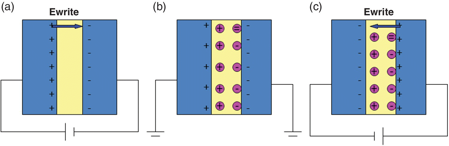
Figure 4.1 Illustration of different fields in P(VDF‐TrFE) FeRAMs: (a) applied write field, (b) the resulting imprinted field, and (c) the switching write field.
Based on Y. Hou (E. China University of S&T), Applied Physics Letters, 102 (6), 063507, February 2013 [1].
The imprint time is the time to form internal domains in response to an externally applied field. It was found that the effective fields and charge trap states in the ferroelectric layers were responsible for the switching behaviors observed. This permitted designating a protocol for copolymer FeRAM.
Using P(VDF‐TrFE‐CFE) terpolymer for fast NV memory was discussed in February of 2013 by Nanjing University [2]. P(VDF‐TrFE‐CFE) terpolymer thin film together with a small amount of chlorofluoroethylene (CFE) was considered for thin film nonvolatile memory. One of the issues with P(VDF‐TrFE) copolymer is the high operating voltage required to store charges due to the high activation energy required for nucleation and domain wall motion of anti‐parallel domains and the slow polarization switching. The use of the terpolymer thin film with a small amount of CFE destabilized the long range ordered and strongly correlated ferroelectric domains of the copolymer. Illustrations of the domains of the copolymer and the terpolymer are shown in Figure 4.2.
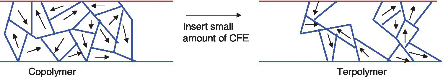
Figure 4.2 Illustrations of domains of copolymer and terpolymer. The terpolymer was obtained by inserting a small amount of chlorofluoroethylene (CFE) in the copolymer.
Based on X. Chen et al. (Nanjing University), Applied Physics Letters, 102 (6), February 2013 [2].
Integration of the P(VDF‐TrFE‐CFE) terpolymer with a small amount of CFE can lead to a low voltage operation and a high read and write speed. A stack of Au/P(VDF‐TrFE‐CFE)/Au was used. The polarization switching voltage for a 50 nm thick film was down to 1 V. The writing–erasing procedure was reversible and the device had a high signal‐to‐noise ratio and high storage capacity. The polarization state of the terpolymer was stable, as required for a data storage device. The switching behavior was thought to be due to the reduced polar domain size and also to the energy cost of domain wall motion during electrically polarized switching decreases.
Determining data retention in thin P(VDF‐TrFE) cells was discussed in July of 2013 by the University of Applied Science of Jena [3]. A technique for determining data retention in thin P(VDF‐TrFE) cells and potentially for nondestructive readout of ferroelectric memory cells was discussed [4]. Data retention tests are normally based on the application of read pulses to a ferroelectric sample while the charge response is recorded. Since a read flips the cell to the opposite state continuous recording of retention after read is not possible.
A new approach was used to determine the state of a ferroelectric cell based on the non‐destructive readout of the remnant polarization by measurement of small signal dielectric nonlinearities. The temporal development of the remnant polarization is directly accessible from the measured first and second harmonics in the current response to a small sinusoidal voltage signal. This technique has been used to study the retention of thin VDF‐TrFE copolymer films of molar ratio 70/30 with thickness below 200 nm.
Nonvolatile memory using an InZnSiO active channel and ferroelectric gate insulator was discussed in July of 2013 by KyunHee University [4]. Thin film transistor nonvolatile memory characteristics were considered for a hybrid gate stack using a solution processed indium‐zinc‐silicon oxide channel and an organic Fe‐(P(VDF‐TrFE)) ferroelectric gate insulator. Device properties such as field‐effect mobility, program speed, and retention were improved by controlling the InZnSiO channel composition of silicon. The use of silicon in the InZnSi x O channel layer modulated the carrier concentration and helped reduce defect density in the channel. It was found that the devices with InZnSiO of 2 mol% Si content showed the best performance. The subthreshold swing was 772 mV/decade, the memory window was 11.9 V, and the ON/OFF current ratio was 5.7 × 10⁵. By including the correct amount of silicon the trade‐off between carrier concentration and defect densities in the channel were optimized along with the program speed, endurance, and data retention.
A graphene‐ferroelectric device for multivalued memory systems was discussed in July of 2013 by the University of Texas Dallas [5]. A graphene‐FE hybrid device was considered for use as a multivalued memory system. The multilevel NVM system used a dual‐gated single layer graphene FET with a polymer ferroelectric as the top‐gate dielectric and a linear bottom‐gate dielectric. The multiple memory states were represented by various levels of graphene channel resistance resulting from changing the doping type and the number of p–n junctions in graphene. This was accomplished by controlling the polarity of the domains in the ferroelectric thin film using a biased metal‐coated atomic force microscope tip. A five level memory was demonstrated with resistance change between the lowest and highest state greater than 200%.
Switching and imprint for ferroelectric poly(vinylidene fluoride‐trifluoroethylene) P(VDF‐TrFE) copolymer was discussed in December of 2013 by the East China University [6]. High speed switching and improved imprint behaviors for poly(vinylidene fluoride‐trifluoroetylene) copolymer ultrathin films were explored with various pulse and unipolar poling processes. The analyses showed that the properties were dependent on the direction of the switching and unipolar poling field. These results provide another method for designing an optimum protocol for FeRAM based on P(VDF‐TrFE) copolymer ultrathin film.
FeRAM can be made of ZnO nanowire transistor (P(VDF‐TrFE) FeRAM on glass substrate. In January of 2014, Cambridge University discussed a fast ferroelectric NVM based on a top gate ZnO nanowire (NW) transistor made on a glass substrate [7]. The ZnO NW channel was spin‐coated with a ferroelectric poly(vinylidenefluoride‐co‐trifluoroethylene) P(VDF‐TrFE) layer acting as a top‐gate dielectric without a buffer layer. Electrical conductance modulation and memory hysteresis were done using a gate electric field‐induced reversible electrical polarization switching of the P(VDF‐TrFE) thin film. The device showed a 16.5 V memory window, a high drain current ON/OFF ratio of 105, a gate leakage current <300 pA, and excellent retention characteristics for over 104 s.
Temperature dependence of the imprint in P(VDF‐TrFE) copolymer was discussed in March of 2014 by Shanghai University of Engineering Science. The temperature dependence of the imprint in P(VDF‐TrFE) copolymer thin film capacitors was studied [8]. Characteristics of the imprint as a function of different temperatures and annealing processes were noted.
It appeared that the temperature‐induced shift of the imprint rate was limited for all the investigated temperature conditions and that this low shift is primarily associated with the competition between the trap states increasing and the detrapping process induced by the temperature increasing. The anneal temperature‐dependent imprint rates in the polymer chains have been analyzed and the annealed cell shows a low imprint rate after 104 switches at an annealing temperature above 100 °C. The internal electric fields for these processes were studied and it appeared that the effective fields and charge trap states in the ferroelectric layers were strongly responsible for the switching behaviors.
Flexible memory devices with amorphous‐InGaZnO (a‐InGaZnO) thin film memory transistor (TFT) and copolymer ferroelectric P(VDF‐TrFE) gate insulator were discussed in April of 2014 by the Institute of Technology, Zurich. Future flexible electronic systems require memory devices that combine low power operation and mechanical flexibility [9]. Mechanically flexible a‐InGaZnO memory TFT with a P(VDF‐TrFE) gate insulator were investigated. A schematic cross‐section of an IGZO memory TFT with a P(VDF‐TrFE) gate insulator layer is shown in Figure 4.3.
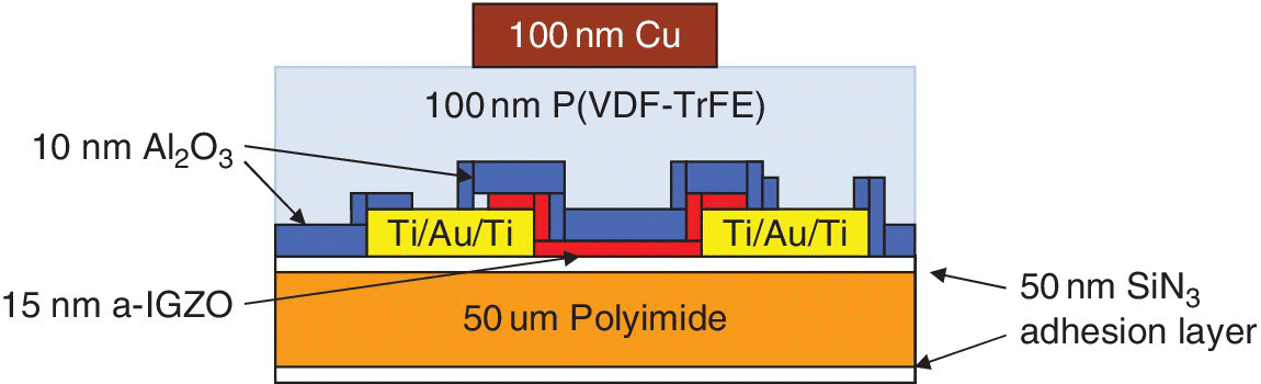
Figure 4.3 Schematic cross‐section of a flexible a‐InGaZnO memory TFT with a P(VDF‐TrFE) gate insulator layer.
Based on L. Petti et al. (IT Zurich), IEEE Trans. on Electron Devices, 61 (4), April 2014 [9].
Memory operation had a memory window of 3.2 V and an ON/OFF ratio of 1.5 × 10⁶. The mobility of 8 cm2/(V s) and the ON/OFF current ratio of 107 were comparable with the values for reference TFTs made on the same substrate. In order to use a memory TFT in flexible applications, their behavior under mechanical strain must be understood. In this study, flexible memory and reference TFTs were characterized with bending radii down to 5.5 mm. Tensile strain caused negative threshold voltage shifts and increased the drain current while compressive strain resulted in the opposite effects.
Memory TFTs compared with reference TFTs show up to 8 times larger threshold voltage shifts and 17 times larger drain current variations. It was shown that the strain‐dependent properties of a‐IGZO can only explain the shifts observed in reference TFTs while the variations in memory TFTs are primarily caused by the piezoelectric properties of P(VDF‐TrFE).
Memory operation was shown with a memory window of 3.2 V and a memory ON/OFF current ratio of 1.5 × 10⁶ for a gate source voltage sweep of ± 6 V. Tensile strain caused a negatively shifted threshold voltage and an increased drain current. Compressive bending resulted in a positive threshold voltage shift and a decreased drain current. Shifts in the Fe‐TFTs were caused by a superposition of the strain‐induced dependence of the polarization in the piezoelectric P(VDF‐TrFE) and the strain‐dependent IGZO properties. These shifts should be considered when designing future flexible memories. These devices had full memory operation down to a bending radii of 5.5 mm, which makes them applicable to use as flexible memories.
In September of 2014 the University Catholique de Louvain discussed the fabrication of an organic FeFET using a ferroelectric gate dielectric made of nanostripes, which are formed by nanoimprinting P(VDF‐TrFE) over a layer of semiconducting poly(triarylamine) [10]. The imprinting process results in the ferroelectric having a decreased switching voltage by a factor of about 1.5. This in turn results in a decreased operating voltage for the nanostripe material compared to a reference FeFET with a continuous ferroelectric layer. The transistor consists of a large number of nanostripe‐gated transistors, which are in parallel. This offers the potential for a significant size reduction in organic FeFETS.
Flexible 2T2C FeRAM can be made with TFT and P(VDF‐TrFE) copolymer. In October of 2014, Micron Technology and the University of Texas, Dallas discussed a 2T2C FeRAM in a low temperature fully integrated process for an FeRAM memory array for flexible electronics applications [11]. The cell used cadmium sulfide as the semiconductor material for n‐channel TFT transistors and P(VDF‐TrFE) copolymer as the ferroelectric material. At VDD = 5 V a voltage difference of about 1 volt between the high and low states is achieved at the output of the sense amplifier. Both of the materials used in this memory are compatible with low temperature processing while maintaining good device performance. The low temperature processes have TFTs with high mobility of 9.3 cm2/(V s), ON/OFF ratio of 108 at 20 V and 0 V, and ferroelectric capacitors with high switching polarization. The low temperature processed FeRAM was based on 2T2C architecture using P(VDF‐TrFE) for the capacitor and CdS for the TFT. Small FeRAM arrays of 4‐bit, 16‐bit, and 64‐bit capacity have been made and a 1 V voltage difference output from the sense amp has been achieved on a 4‐bit FeRAM array. The array is patterned using photolithographic processes compatible with flexible electronics system integration. A cross‐sectional view 2T2C FeRAM array process is shown in Figure 4.4.
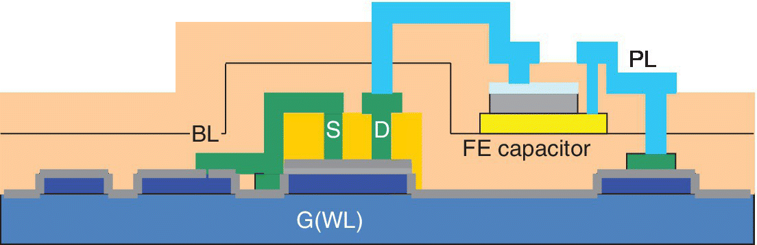
Figure 4.4 Cross‐sectional view of low temperature process for 2T2C FeRAM array.
Based on D. Mao et al. (Micron., University of Texas), IEEE Trans. on Electron Devices, 61 (10), 3442, October 2014 [11].
The FeRAM array is made on a silicon substrate with 500 nm SiO2 on top for electrical isolation. The TFT is made using CdS as the semiconductor and FE‐capacitor of P(VDF‐TrFE) copolymer. The highest temperature in the process is the TFT anneal at 300 °C.
P(VDF‐TrFE) copolymer organic FeFET and FeRAM characterization were discussed in October of 2014 by Slovak University of Technology [12]. The MIM structures were used to investigate the ferroelectric properties of FeFET and FeRAM. The I–V and C–V curves representing characteristics were analyzed. The MIM device fabrication and characterization was described including saturated polarization, maximum electric field intensity, critical electric field, and relative dielectric constant.
4.2.2 Printable Ferroelectric Embedded Memories
Flexible electronics has potential for use in rollable and foldable displays, smart patches and smart packaging on paper and plastic substrates. Printing sensors and transistors is an attractive idea since large area electronics can be fabricated roll‐to‐roll at low temperatures on plastic substrates. Due to the limitations of fully printed electronics systems in performance, today there is focus on both a fully printed electronics system and on integration of large area flexible electronics with chips. Most of the interest is in inexpensive plastic substrates although there is still some interest in metal foil and glass [13].
There has been progress in printed sensor elements, printed logic, and some printed logic and memory built with complementary n and p polymer semiconductors. Inkjet printing has been used for prototyping since short runs are possible with immediate turnaround. Many printing techniques are compatible with large area or roll‐to‐roll processing. Printing is valuable for those applications with a large area and for which only moderate complexity is required.
In December of 2012, Thin Film Electronics demonstrated a prototype label that replaced a disposable printed electronic tag with a low cost printed sensor system [14–16]. These tags could be used to replace bar codes in the Internet of Things”. The printed system included memory and sensor, and logic was designed to detect whether temperature thresholds had been exceeded. The data was recorded digitally in a nonvolatile memory for later retrieval. This technology is expected to compete with active RFID tags that have rewritable memory.
The prototype of an integrated printed electronic tag was based on rewritable ferroelectric memory. These labels could be used for tracking shipments of pharmaceuticals and perishable foods. These tags could be used to replace bar codes in the “Internet of things”. One application combines a tracking tag with a temperature sensor so a shipped package with perishable goods could be confirmed to have stayed within the correct temperature range during shipment. The circuit was printed with a technology similar to the inkjet printer, which sprays electronic circuitry on to thin film surfaces. It included the electronics for memory, sensors, such as temperature sensors, and a processor. It was expected to be a few years before the system is in mass production. The tags would be at a lower cost than current RFID tags. The prototype was built by PARC, Thin Film, and PST Sensors, who provided the printed thermistor, and Acreo, who provided the electrochromic display.
The tag has multiple electronics functions including memory, logic, and temperature sensor. The devices worked together by sensing temperature thresholds and writing to memory. A polymer ferroelectric memory is used in these tags. The data triggers a display through external circuitry.
Integrating memory, logic, sensors, and displays using printed circuitry is critical for delivery of cost‐effective mass produced printed electronic devices. Additional circuitry, including a timer function and wireless communication, were expected to be added to the system. The technology was expected to compete with active RFID tags that have rewritable memory.
In June of 2013, various French labs also demonstrated the required components of organic logic and complementary memory circuits [17]. The circuits were made with organic N‐type and P‐type transistors. Complementary NAND and NOR gates were made and characterized. An SRAM was made and an edge triggered flip‐flop was made of six organic two input and three input NAND gates consisting of 26 organic transistors with an area of 170 mm2. The maximum operating frequency of the flip‐flop was 220 Hz with a ±20 V power supply. The circuits were made using an organic sheet‐to‐sheet process at ambient temperature. Electrical characteristics were stable. A model was developed to represent the circuit performance. Target application was low cost RFID circuits replacing barcodes. Sheet‐to‐sheet printing was used since it is low cost and has good alignment accuracy.
Complementary CMOS‐like ICs on plastic foils have historically been difficult to make due to lack of air stable N‐type organic semiconductors. The NOR and NAND gates, in this case, were made using both N‐type and P‐type organic transistors. They had full rail‐to‐rail behavior with only a small offset due to the P‐type having a higher mobility than the N‐type. The use of both N‐ and P‐type transistors permitted rail‐to‐rail curves with no current consumption except during switching. The I on/I off ratio was >105. No vacuum process was required during the sheet‐to‐sheet printing. The circuit worked with a ±20 V power supply and ran at 220 Hz. An SRAM was also made with six organic transistors using the same manufacturing process as the rest of the sheet. The transient characteristics of the SRAM were determined. A schematic cross‐section of the screen‐printed complementary gate is shown in Figure 4.5.
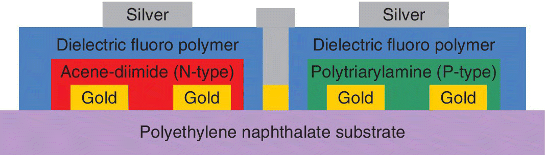
Figure 4.5 A schematic cross‐section of the screen‐printed complementary gate.
Based on M. Guerin et al. (Aix‐Marseille U., IM2NP, CNRS, IM2NP,LTEN‐LCEI, CEA‐Grenoble), IEEE Trans. on Electron Devices, 60 (6), June 2013 [17].
The CMOS semiconductor devices were made on a 125 µm thick polyethylene naphthalate substrate. A 30 nm Au source/drain layer served as a first level connection and was formed by laser ablation. The P‐type transistor was a polytriarylamine derivation and the N‐type was acene‐based, diimide. Together they were 100 nm thick. An 800 mm thick dielectric fluoropolymer was screen printed and annealed. Then the gate layer was screen printed using a 5 µm thick silver paste. This gate layer also served as a second connection layer. A final annealing was done at 100 °C. Process alignment was around ±25 µm. The process was performed in air.
The 6 T SRAM was made of the organic transistors as shown in the circuit schematic in Figure 4.6. To perform a write, the WL is set to VDD, then the BL is set to VDD, and BL is set to VSS. The point B is then pulled to VDD. When the WL is grounded, the SRAM is isolated with the data stored in it. This circuitry can be used to form an operational RFID tag.
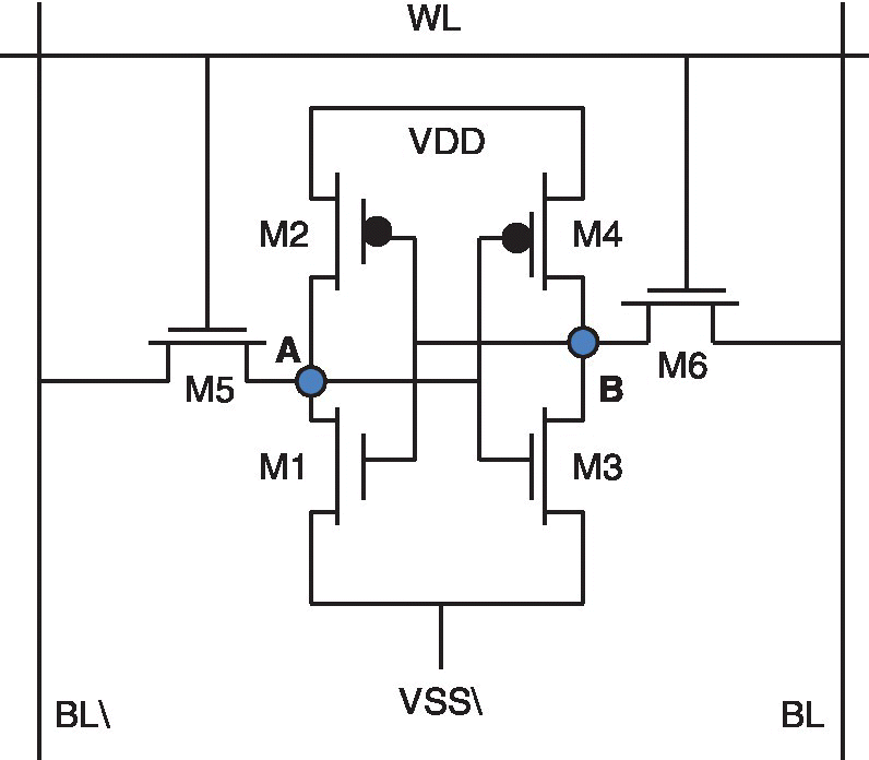
Figure 4.6 6T SRAM of organic transistors.
Based on M. Guerin et al. (Aix‐Marseille University, IM2NP, CNRS, IM2NP,LTEN‐LCEI, CEA‐Grenoble), IEEE Trans. on Electron Devices, 60 (6), June 2013 [17].
An 8b general purpose MCU was made in a hybrid oxide‐organic complementary thin film technology. This 8b MCU in hybrid oxide‐organic thin film was discussed in February of 2014 by IMEC, KU Leuven, Panasonic, Evonik, and Holst [18]. The n‐type transistors were based on a solution‐processed n‐type MOS and the p‐type transistors used an organic semiconductor. The high mobility n‐type semiconductor and the complementary logic permitted a greater than 50 times speed improvement. The robustness of the design permitted a complete standard cell library. The MPU was in two parts: a processor core chip and an instruction generator. The instruction generator has instructions stored in a write‐once‐read‐many (WORM) memory, which is formatted using a inkjet printing step to produce a print‐programmable ROM or PPROM. The entire printing process was performed at temperatures below 250 °C. A block diagram of the PPROM is shown in Figure 4.7.

Figure 4.7 Block diagram of print programmable ROM.
Based on K. Myny et al. (IMEC, Panasonic, KU Leuven, Evonik, Holst), ISSCC, February 2014 [18].
The hybrid oxide‐organic complementary processor had a core transistor count of 3504 and the PPROM transistor count was 852. The area was 1.2 × 1.86 cm2. Technology was 5 µm feature size p‐type Pentacene with n‐type metal oxide. Performance at V min of 6.5 V was 2.1 kHz at 12 V VDD. Mobility was –0.15 cm2/(V s) (p‐type) to 20 cm2/(V s) (n‐type).
In January of 2015, Xerox and Thinfilm announced a deal to mass‐produce their thin film “printed electronics”. Under the agreement, Thinfilm would be permitted to print up to a billion chips a year for various smart connected devices such as processors, memory, and sensors for the Internet of Things [19]. The smart labels for packages were expected to sense and store data for a tenth to a hundredth of the cost of conventional electronics. Options could be a temperature sensor printed on a smart label that can indicate the maximum temperature attained. Near field communications (NCF) technology could be used to read the sensors and transfer the data to the retailer using an Internet cloud. Smart labels can also be attached to perishable food or medicines.
In September of 2015, Xerox and Thinfilm discussed bringing printed memory to market [20]. Two types of printed memory were considered with or without cryptographic security. The Xerox printed memory a
the time was a small flexible label with 4 to 36 bits. It did not require a battery or a power source but did require a reading device to extract the data. Key applications considered were smart consumables, expensive fashions, and brand protection. The plan was to make the Xerox printed memory in Xerox’s Webster, New York, plant. The reader was still under development.
Labels without memory could already be printed on to plastic, which could be pasted on to a consumer product as a smart label, as shown in Figure 4.8. The label can be scanned with a smartphone using an application that permits reading of the QR code on the label.

Figure 4.8 Illustration of a bottle of wine with a barcode, QR Code, and ID number, which permits the consumer to use a smartphone to ensure the authenticity of the wine and gain information about it. Photo by B. Prince.
In September of 2015, Xerox launched printed memory products intended to combat counterfeiting of branded and governmental products [21]. These labels could collect and store information about the authenticity and condition of products in 36 rewritable bits. A second product, printed memory with cryptographic security, included a unique encrypted printed code in the memory, which can only be read by an authorized person with a reader that could interface with a secure smartphone application. The cryptographic security feature was developed by Xerox PARC and is an added feature in the uniquely encoded printed memory label, which could ensure the integrity of a product from the factory to the consumer.
In January of 2016, Xerox announced it was setting up a 1.3 billion capacity smart label print line in Webster, New York [22]. Operating at full speed, this line was expected to have an annual output of over 1 billion smart labels. These labels are intended to be sold by Xerox as part of its diversification into the printed electronics market.
In June of 2016, Thin Film Electronics announced it was modifying a production line in Webster, New York, to produce memory labels [23]. These labels can add low cost intelligence to high end objects like wine bottles or perishable foods. They can store up to 36 bits of information, which enables 68 billion distinct data combinations. The label is written and read off‐line and the reader needs to make physical contact. Data retention is up to 10 years. The label includes cryptographic capability and is combined with bar code technology. These are printed on the substrate. The data can be written and read using a contact reader that interfaces with a smartphone.
In March of 2017, Thin Film Electronics was making an NFC smart label that was printed and put on a bottle of Johnnie Walker Blue Label scotch [24]. This label permits communication with the consumer. The label authenticates the bottle, shows if it is counterfeit, and, using NFC, it can connect the consumer’s smartphone to a web page with personalized promotion or a direct line to the company. The solution was in field trials in 2017. Another use of a printed smart label was a web site that sells beer to local microbreweries in the San Francisco Bay Area. The Thinfilm smart label is put on the beer bottle. The consumer taps an NFC smartphone on the label and it takes you to a video that describes the beer. The smart label would permit the beer company to interact with the customers directly rather than through expensive ads.
In October of 2016, Hewlett Packard and Hong Kong University of S&T discussed a summary overview of the design of printed circuits using thin film transistors (TFTs) [25]. A new design style, called Pseudo CMOS, was discussed, which could handle several design challenges of TFTs. Examples of Pseudo CMOS circuits designed for various applications were shown. These applications included: energy, healthcare, biomedical, and near field communication (NFC) tags.
Characteristics of the various other TFT technologies discussed and their characteristics available for printed circuits are shown in Figure 4.9. The various TFT technologies used processes that included: lithography, shadow mask, inkjet printing, and shadow mask lithography. Feature size ranged from 8 µm for amorphous silicon to 50 µm for carbon nanotubes. Supply voltage went as low as 2 V and mobility from 1 cm2/(V s) for amorphous silicon to 25 cm2/(V s) for carbon nanotubes.
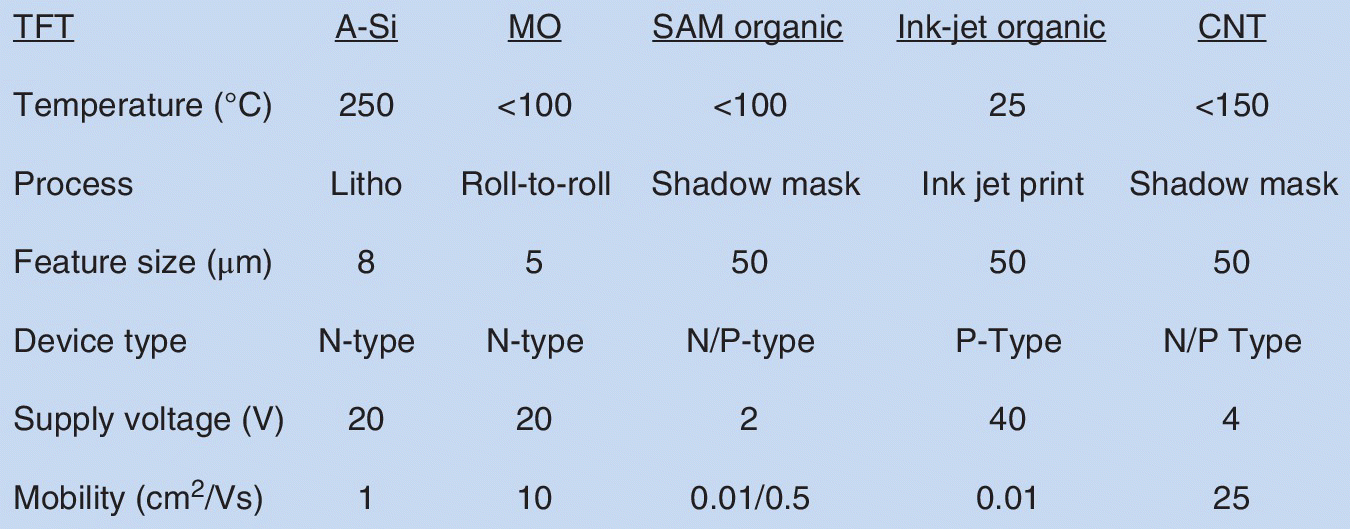
Figure 4.9 Characteristics of the various TFT technologies including: amorphous silicon, metal oxide RRAM, self‐assembly monolayer (SAM) organic and inkjet organic.
Based on T.C. Huang et al. (Hewlett Packard, Hong Kong University.of S&T), NOCS, October 2016 [25].
4.2.3 IoT Applications of Thin Film Ferroelectric Memory
In June of 2015, Kyung Hee University and the Electronics and Telecom Research Institute, Daijeon, discussed a liquid crystal display pixel architecture using two oxide thin film transistors (TFTs), two ferroelectric memory TFTs, and two capacitors, as shown in Figure 4.10 [26]. Both TFTs used InGaZnO film as an active layer. The ferroelectric MTFT showed hysteresis due to the ferroelectric gate insulator permitting it to operate as a memory. A low refresh rate was achieved by using oxide TFTs with extremely low leakage currents; however, there was an issue with flicker due to the current leakage through the liquid crystal and the flexoelectric effect of the liquid crystals.
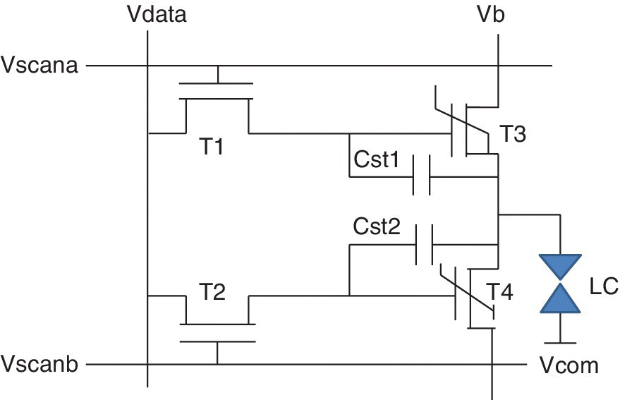
Figure 4.10 Schematic circuit diagram of liquid crystal display pixel architecture using two TFTs, two ferroelectric TFTs, and two capacitors.
Based on S.H. Lee et al. (Kyung Hee University ETRI, Daijeon), IEEE Electron Device Letters, 36 (6), 585, June 2015 [26].
A 6 × 5 pixel LCD was fabricated. The memory window of the Ferroelectric MTFT was 5 V with a gate‐voltage sweep from –20 to +20 V. After programming the memory, the LCD operated at a 0.5 Hz refresh rate. The ferroelectric MTFT maintained the on or off states. These states selected voltages to display black or white pixels, thereby maintaining flicker‐free images regardless of LC leakage.
In October of 2015, Kobe University and ROHM discussed a ferroelectric‐based nonvolatile flip‐flop (nvFF) for use in wearable healthcare systems [27]. In this nvFF, coupled FE capacitors with complementary data storage were developed. By using complementary stored data in coupled ferroelectric capacitors, an 88% capacitor size reduction was achieved while still maintaining a wide read voltage margin of 240 mV at 1.5 V. This resulted in 2.4 pJ of energy with 10 year 85 °C data retention. The access speed for the ferroelectric capacitors could be changed according to the required retention time and was 1.6 µs for 10 year data retention and 170 ns for 10 hour data retention. A short data retention is okay for power gating applications.
The resulting nvFF was used in a 32‐bit CPU in a wearable electrocardiogram (ECG) sensor LSI. The 32‐bit CPU core had an NVFF and a 16 KB ferroelectric‐based NVRAM for instruction and data caches. Since the frequency range of vital signals is low, both standby power reduction and sleep time maximization were important for reducing system level power. The standby current could be cut when the CPU core transited to the deep sleep state. In deep sleep, the data in the memory and the register values of the CPU core in the nvFF were stored sequentially in the ferroelectric capacitors. Thus 87% of the total power dissipation during measurement of the heart rate was reduced, with 64% area overhead using a 130 nm CMOS process and PZT thin films for the ferroelectric nvFF.
In January of 2016, Kyung Hee University and the Electronics and Telecom Research Institute discussed a new circuit architecture using NVM thin film IGZO transistors and oxide‐based TFT for low power consumption and small size for use in dynamic driving circuit applications [28]. The top gate used ferroelectric poly(vinylidene flouride‐triflouroethylene) gate insulator along with Al2O3/InGaZnO active layers. The memory device characteristics were confirmed for the fabricated nonvolatile memory TFT. The feasibility of a low power display driver circuit using embedded nonvolatile memory TFTs was confirmed.
4.3 Polymer Ferroelectric Tunnel Junctions
Ultrathin BaTiO3 ferroelectric tunnel junctions were studied in 2015 by the National University of Singapore and Trinity College Dublin using interface engineering [29]. States were changed using voltage in ferroelectric tunnel junctions (FTJs) since this permits lowering the switching energy of the memory. Enhanced tunneling electroresistance in FTJs can be achieved by using asymmetric electrodes or by introducing metal–insulator transition layers. The effect of each interface on FTJ performance was studied using varying asymmetries of the electrode and ferroelectric interfaces. High tunneling electroresistance (TER) of about 400% could be achieved with BaTiO3 layer thicknesses down to about 0.8 nm. The results showed that band offsets at each interface in the FTJs control the TER ratio. The off‐state resistance (Roff) was found to increase much more rapidly with the number of interfaces than the on‐state resistance (Ron). These results were found promising for future low energy memories.
Polymer ferroelectric tunnel electroresistance was discussed by CAS, University of Paris Saclay, University of Paris South, and East China Normal University in May of 2016 [30]. The application being considered was organic electronics for large area applications such as rollable displays or electronic paper that requires a simple, low power organic memory that can be written, erased, and read electrically. The NVM used ferroelectric polarization of an organic tunnel barrier. The device encoded the stored information and set the read out tunnel current. Piezoresponse force microscopy showed that films as thin as one or two layers of ferroelectric poly(vinylidene fluoride) (PVDF) remained switchable with low voltages. Submicrometer technology junctions based on these films displayed tunnel electroresistance (TER), reaching 1000% at room temperature. This was explained by ferroelectric switching and by electrostatic effects of direct tunneling.
An opportunity was provided to develop low‐cost, large‐scale arrays of organic ferroelectric tunnel junctions on silicon or flexible substrates. The electronic transport mechanism was more fully explored by observing room temperature TER in organic FTJs using ultrathin films. It was demonstrated that the ferroelectric switching could be sustained down to one layer and that charge transport across monolayers and bilayers of PVDF‐based FTJs proceeds by direct quantum mechanical tunneling transport.
4.4 Types and Characteristics of Polymer Resistive RAMs with Flexible Substrate
4.4.1 Overview of Polymer Resistive RAMs with Flexible Substrate
RRAMs can be made with low cost materials and simplified manufacturing procedures. Use of the RRAM for IoT applications is discussed in terms of process variation produced performance and yield limitations. Flexible polymer RRAMs are being developed based on Parylene‐C, which have good chemical stability and CMOS process compatibility. Copper atom switches can be made with a polymer solid electrolyte and with chalcogenides and exhibit a high ON/OFF current ratio. Inorganic thin film RRAMS have the potential for integration on flexible substrates with a low voltage read and multilevel operation.
4.4.2 Parylene‐C‐Based Resistive RAM
Parylene‐C based RRAMs in an 8 × 8 cross‐point array were discussed in December of 2012 by Peking University and Princeton University [31]. They discussed the resistive switching behavior of a single component polymer resistive memory using polychloro‐para‐xylylene (parylene‐C) [31]. A sandwiched structure of parylene‐C was made as an 8 × 8 crosspoint array of RRAMs integrated in a CMOS back‐end process. Parylene‐C was expected to be useful in the future for transparent, low cost, flexible NV memory applications. The ON/OFF current ratio of the RRAMs was 107. SET/RESET speed was in the nanosecond range and switching voltages were low. Retention was good. The switching mechanism was studied using Al, Cu, and Ag as active electrodes and Pt as the inert electrode. The read voltage was ±0.2 V. Ion was 10−4 and I off was 10−30. Cell size was 25 µm2. The ON/OFF current ratio was about 107. The currents at different read voltages showed a distinct difference between the ON and OFF states. For V(read) of 0.2 V, I(on) was 10−4 A and I(off) was 10−30 A. For V(read) of –0.2 V, I(on) was 10−3 A and I(off) was 10−30 A.
The RRAM showed good cycling behavior and retention. The resistive switching of the device was attributed to the formation and annihilation of a metallic filament. Since this material can tolerate conventional photolithography and is compatible with a CMOS back‐end process, the device was considered as a potential for hybrid integration with CMOS.
An RRAM with sub‐20 nA reset current was discussed in February 2013 by Peking University [32]. The organic RRAM was based on double layer parylene‐C technology. These devices were fabricated and showed stable bipolar resistive switching behavior and good data retention. Reset current was <20 nA and set current was 0.15 μA. The switching ratio was nearly 105 times that of single layer parylene‐C cells. A schematic view of the Al/parylene‐C/parylene‐C/W cell is shown in Figure 4.11.
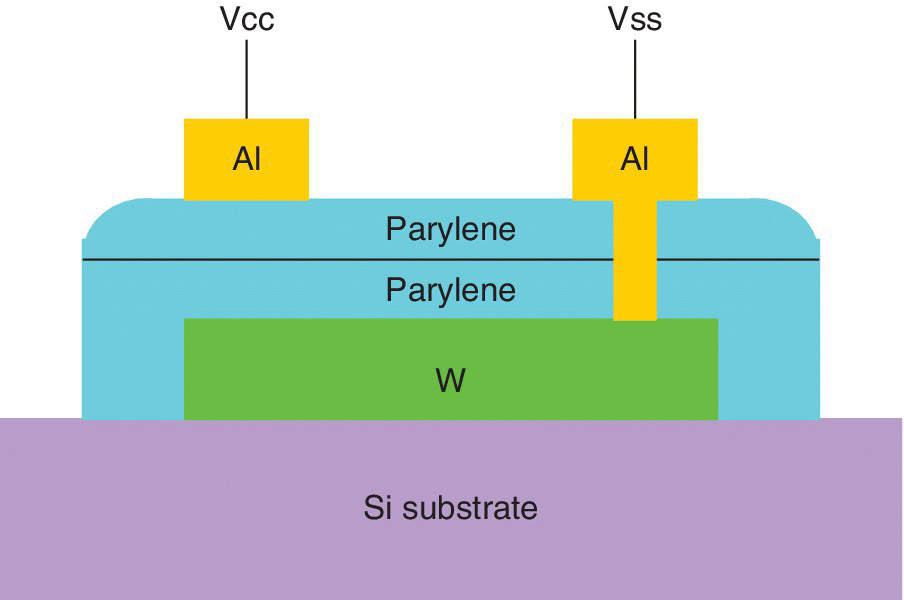
Figure 4.11 Schematic cross‐section of Al/parylene‐C/parylene‐C/W cell.
Based on W. Bai et al. (Peking University), IEEE Electron Device Letters, 34 (2), February 2013 [32].
The bottom electrode (BE) was sputtered W film on a silicon substrate. Parylene‐C film was deposited by room temperature polymer CVD. After an 18 hour exposure to air a thicker parylene‐C film was deposited. An Al top film electrode was deposited and patterned. Bias is put on the top electrode and the bottom electrode is grounded.
The resistive switching mechanism for the single layer parylene‐C device was interpreted as the formation and rupture of metallic filaments. The double layer parylene‐C with thin parylene‐C layer showed a high resistance state (HRS) current due to Poole‐Frenkel emission. The low resistance state (LRS) current was attributed to traps in dielectrics of very thin parylene‐film. The thin layer showed a negative temperature coefficient as opposed to the positive temperature coefficient in single layer metallic filaments. Hopping conduction was also shown in the double layer device, leading to a large internal resistance and a resulting small self‐compliance SET current. The resistance ratio (R hrs/R lrs) > 104. The device showed good retention for 104 s at 85 °C although degradation of the resistance ratio and retention ability was found at 210 °C.
Low cost, low power flexible parylene‐C RRAM was discussed in June of 2014 by IM Peking University, who studied organic resistance memories for future flexible applications [33]. The focus was on a polymer resistance memory device based on parylene‐C. This device had good chemical stability and CMOS process compatibility. It reduced operational current as needed for information storage in many flexible systems.
The switching layer of flexible RRAM can be organic, inorganic, or organic–inorganic. Organic RAMs can be based on various organic materials such as polymers or polymer composites containing nanoparticles. In the parylene‐C RRAM, the device was made on an SiO2/Si substrate or plastic substrate in order to be flexible. The parylene‐C layer is deposited by CVD. This process could be integrated into the BEOL in CMOS technology without contamination. The RRAM device had good NVM characteristics with low switching voltages and a high ON/OFF current ratio larger than 107 at 0.01 V read. The I–V curve of a typical Al/parylene‐C/W device is shown in Figure 4.12.
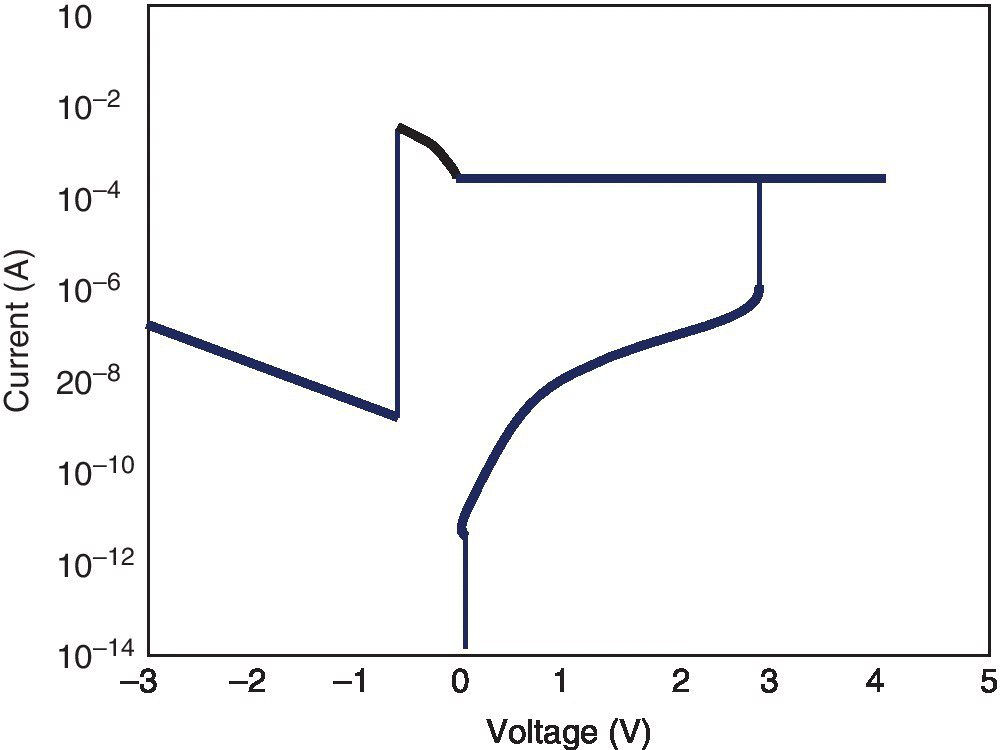
Figure 4.12 Illustration of I–V curve of typical Al/parylene‐C/W RRAM device.
Based on R. Huang et al. (Peking University), ISCAS, June 2014 [33].
This device can be made by a conventional photolithography process. It can switch in nanoseconds and has a high ON/OFF current ratio greater than 107. A double layer parylene RRAM was proposed for future investigation. A parylene‐C RRAM device was shown to be flexible, have low cost and low power, while remaining CMOS compatible.
4.4.3 Cu Atom Switches
The conduction mechanism in a Cu atom switch using a polymer solid electrolyte was discussed by LEAP in December of 2012 [34]. LEAP discussed low temperature characterization of electrical transport in an atom switch, which is also called a conductive bridge RAM. Atom switches and RRAMs both consist of metal–insulator–metal (MIM) structures. For the atom switch, the insulator works as a solid electrolyte that is sandwiched by an oxidizable electrode, of either copper or silver, and an inert electrode, either Ru or Pt. Chalcogenides such as GeSE, Cu2S, and Ag2S have also been used as the electrolyte for an atom switch.
The low resistive ON state with resistance <400 ohms shows metallic conduction along with high residual resistance. In the high resistive OFF state with resistance >108 ohms, the resistance exponentially increases with decreasing temperature due to Poole‐Frenkel conduction. In the intermediate resistance range of about 105 to 107 ohms, the resistance has a small temperature dependence since the electron tunneling is due to Cu residues in a solid electrolyte and is dominant. Metal oxides such as Ta2O5 and TaSiO achieve a reliable OFF state and a high ON/OFF conductance ratio, as needed for programmable switches in reconfigurable LSIs.
The polymer solid electrolyte (PSE) enables the complete collection of the Cu residues without degrading the electrolyte. This results in forming free operation and a high ON/OFF conductance ratio. In the atom switch, the resistance state reversibly switches between dielectric and metallic. Complete collection of the Cu residue from the solid electrolyte was shown to be key for forming free operation and a high ON/OFF conductance ratio.
In September of 2015, LEAP discussed the relationship between speed and low voltage programming of a Cu atom switch [35]. The effect was studied of the composition in the Al1‐x Ti x O y buffer layer, which is sandwiched between the Ru and Cu electrodes below the polymer solid electrolyte (PSE). A schematic cross‐section of the Cu atom switch stack is shown in Figure 4.13.
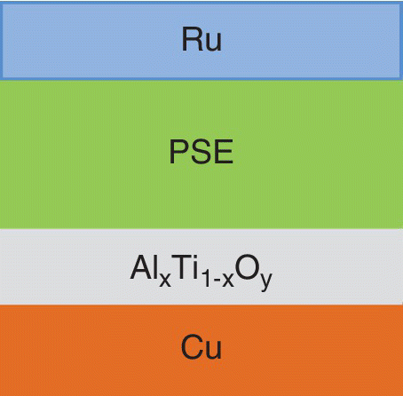
Figure 4.13 Copper atom switch stack with PSE and Al1‐x TixOy layers sandwiched between Ru and Cu electrodes.
Based on N. Banno et al. (LEAP), IEEE Trans. on Electron Devices, 62 (9), September 2015 [35].
To improve the voltage dependence of the switching slope (SS), which determines the time‐to‐on‐state, the Cu ionization rate was increased. This was done by changing the composition ratio of the Al1‐x Ti x O y buffer and PSE to attain a steep SS of 56 mV/decade by eliminating metallic Al residue on the Cu electrode. The operation of an atom switch, a type of conducting bridge RRAM, is illustrated in Figure 4.14.
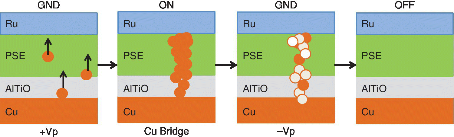
Figure 4.14 Atom switch physical operating mechanism.
Based on N. Banno et al. (LEAP), IEEE Trans. on Electron Devices, 62 (9), September 2015 [35].
Figure 4.14 shows two electrodes with the bottom electrode made of Cu and the top electrode made of Ru alloy sandwiching an AlTiO layer. When a positive voltage is placed on the Cu electrode and the Ru is grounded, a conducting Cu filament forms in the AlTiO between the two electrodes. This is the ON state. If the voltage is reversed, the filament dissolves back into the PSE.
This buffer has 10 ns 2 V programming in a 1 Mb array. Cycle endurance was greater than 103 cycles with an ON/OFF resistance ratio >104. The steep SS is required for conducting bridges used in low power nonvolatile field‐programmable gate arrays (FPGA). The switch was demonstrated in an FPGA, which is an array that can change its circuit configuration by programming switches and their connecting logic blocks.
The two terminal Cu atom switch (CAS) is used with a control terminal. The CAS is made up of two atom switches connected in the opposite direction to each other through a control gate. T1 and T2 are for signal transfers and the control gate (C) is for programming. Figure 4.15 illustrates the signal current for the switch in the (a) ON state and in the (b) OFF state.


Figure 4.15 Signal current for two terminal Cu atom switches (CASs) in (a) ON state and (b) OFF state.
Based on N. Banno et al. (LEAP), IEEE Trans. on Electron Devices, 62 (9), September 2015 [35].
For programming, the terminals are individually connected to + Vp and GND, as shown in Figure 4.16. To program the T1 terminal, +Vp is connected to T1 and GND to C. To program the T2 terminal +VP is connected to T2 and GND to C. The CAS was integrated in a 65 nm CMOS process with a seven‐layer Cu BEOL using two additional masks. The CAS was formed on the edge of two M4 lines.
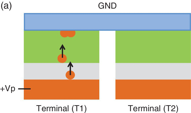

Figure 4.16 Programming the two terminal Cu atom switches (CASs): (a) left side and (b) right side. Based on N.
Banno et al. (LEAP), IEEE Trans. on Electron Devices, 62 (9), September 2015 [35].
A 1 Mb array was made. The two 512Kb arrays were surrounded with peripheral circuits and decoders. The arrays consisted of CAS elements placed at the crosspoints of the bit lines and word lines. The entire Cu bridge dissolves into the PSE and the Cu ions return to the Cu electrode, indicating a forming free operation of the atom switch. More than 1000 cycles of endurance with a 104 ON/OFF resistance ratio were confirmed.
In September of 2015, NEC discussed the ON‐state reliability of a Cu atom switch under current–temperature stress [36]. The DC current–stress tolerance of the ON‐state Cu atom switch was evaluated at high temperatures. It was found that stress due to the current in the RESET direction caused time‐dependent failures as a result of E‐field driven diffusion of the Cu in the conducting bridge. The maximum current per atom switch was found to be 115 μA. The reconfigurable switch block was operated at 500 MHz at 125 °C.
In June of 2016, NEC discussed a Cu atom switch with over 400 °C thermally tolerant polymer solid electrolyte (TT‐PSE) for nonvolatile programmable logic [37]. The Cu atom switch was made in a standard Cu back‐end‐of‐the‐line (BEOL), as shown in Figure 4.17. To achieve switching, hydrocarbons with weak chemical bindings in the PSE were selectively eliminated, resulting in higher thermal stability. Data retention characteristics were confirmed after thermal cycle stress at temperatures ranging from –65 to 150 °C for 1000 cycles. The atom switch was intended as a technology component of reliable reprogrammable logic for future robotic and vehicle applications in high temperature systems.

Figure 4.17 Illustration of polymer solid electrolyte BEOL Cu atom switch (CAS), which is between M4 and M5.
Based on K. Okamoto et al. (NEC), VLSI‐Technology Symposium, June 2016 [37].
A SET/RESET switching model of a Cu atom switch based on electrolysis was discussed by NEC in April of 2017 [38]. A nanometer thick layer of solid electrolyte gave an electric field of 3.3 MV/cm in the solid electrolyte at 2 V. This enabled ionization of Cu and the formation of a Cu bridge. It was found that the switching voltage depended on the resistance of the electrolyte. A compact model was used for estimating the resistance of the Cu atom switch programmed by various conditions.
4.4.4 Inorganic Thin Film Resistive RAMs on Flexible Substrates
An Ni/GeO x /TiO y /TaN RRAM on flexible substrate was discussed in April of 2013 by NCTU, NTNU, and IM‐CAS [39]. The dielectric substrate was GeO x /TiO x . The top and bottom electrodes were Ni/N‐rich TaN. Performance characteristics were 30 μW switching power (9 μA at 3 V, –1 μA at –3 V), 105 cycles of endurance, and good retention at 85 °C. These properties were thought due to: bulk transport properties by tunneling between traps, forming‐free resistive switching, and low power switching. It is difficult to integrate a floating gate or charge trapping Flash memory on a flexible substrate due to the degraded gate oxide quality at low temperature. The RRAM, however, can be made using a low temperature process and simple structure that can be used in the flexible electronics application.
A typical I–V sweep cycle curve of the Ni/GeO x /TiO y /TaN RRAM device on polyimide with an area of 11 300 µm2 is illustrated in Figure 4.18. A V read at 0.5 V is shown with the low resistance state (LRS) and high resistance state (HRS) indicated.
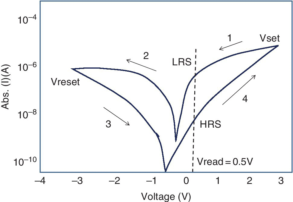
Figure 4.18 Illustration of swept I–V curve of Ni/GeOs/TiOy/TaN flexible RRAM device on flexible polyimide. A read is shown at 0.5 V with low resistance state (LRS) and high resistance state (HRS) shown.
Based on K.I. Chou et al. (NCTU, NTNU, IM‐CAS), IEEE Electron Device Letters, 34 (4), April 2013 [39].
The NVM device had adequate performance on a low cost flexible substrate. The device data showed I
set at V
set of 9 μA at 3
V and I
reset at V
reset of –1 μA at –3 V. Switching power was 30 μW. The ON/OFF current ratio was 30. Electrical endurance was 105 cycles and retention time was 104 seconds at 85 °C. Resistive switching was forming‐free and set/reset currents were low.
Inorganic–organic RRAM with uniform, multilevel cell (MLC) operation was discussed in April of 2014 by IM Peking University [40]. The concern was for improving uniformity and multilevel operation for an HfO x /parylene‐C hybrid RRAM device. Measurements showed that the switching parameter uniformity of this hybrid device was significantly improved compared to pure parylene‐C RRAM memories. A current/voltage (I–V) curve of a Pt/HfO x /parylene‐C/Al structure is shown in Figure 4.19.

Figure 4.19 Illustration of I–V curve of Pt/HfOx/parylene‐C/Al structure.
Based on Y. Liu et al. (IM Peking University), VLSI‐TSA, April 28, 2014 [40].
The resistive switching mechanism was attributed to formation and rupture of the metallic filament in the parylene layer. By inserting an HfO x layer, the filament is localized and good uniformity and stability are achieved. The organic hybrid devices are capable of low voltage operation with V set = 2 V, V reset = –0.6 V, and a high ON/OFF current ratio >103. Since the device is highly uniform and has a large ON/OFF current ratio, the MLC storage capability is good and good retention was demonstrated. It was concluded that the device has potential in flexible, high density NV memory applications.
Flexible electronics devices are interesting due to characteristics such as low cost, low fabrication temperature, light weight, and flexibility. In July of 2014, National Dong Hwa University discussed resistive switching memory with good performance to be used with flexible electronics [41]. In this study an inorganic Al/Al2O3/ZrO2/Al flexible resistive switching memory was made at room temperature. Inorganic materials tend to have relatively high mechanical strength, high humidity resistance, high durability, and good stability compared with organic materials.
To make the switching memory, an Al bottom electrode was deposited on a polyethersulfone plastic substrate; then ZrO2 and Al2O3 resistive switching layers were deposited on the bottom electrode. Al top electrodes were made on the Al2O3 layer through a shadow mask. All deposition steps were done at room temperature by RF sputtering. A resistive switching filamentary model of the flexible device was developed, as illustrated in Figure 4.20 showing (a) SET and (b) RESET. Resistive switching endurance was over 100 times with stable resistive switching characteristics. Flexibility and nonvolatility characteristics of the device were shown.
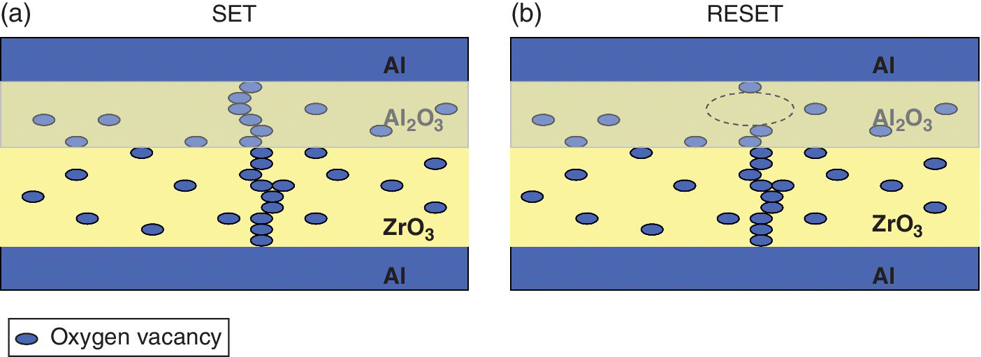
Figure 4.20 A resistive switching filamentary model of an Al2O3/ArO3 flexible device: (a) set and (b) reset.
Based on C.C. Lin (NDHU), IEEE Trans. on Magnetism, 50 (7), July 2014 [41].
4.4.5 IZO and IGZO Resistive RAM Memories
High density and high performance logic with embedded NVM using amorphous InGaZnO (a‐IGZO) TFTs was discussed in July of 2013 by NCTU [42]. High performance logic and NVM applications were served using the same device structure. This opened the opportunity of low cost embedded memory for system‐on‐plastic integration. The use of a‐IGZO TFT embedded NVM could permit several compact memory array architectures with high bit density.
Logic circuits have been shown using a‐IGZO TFT including logic gates, ring oscillators, shift registers and SRAM. The a‐IGZO TFT technology is therefore a potential platform for monolithic system‐on‐plastic (SoP) integration, which offers low cost, light weight, high density, large area, and mechanical flexibility. Embedded NVM devices have been suggested for use with flexible a‐IGZO TFT circuits. Charge storage NVM using both floating gate and charge trapping have been shown. RRAM can be implemented in back‐end metallization processes but it requires extra process steps and masks, which lower yield and add to cost.
An RRAM in the standard a‐IGZO process was shown to combine the advantages of low cost integration, high bit density, and flexible memory characteristics, making it suitable for SoP applications. A four mask a‐IGZO TFT with a top gate top contact structure was made on a flexible polyimide substrate in both coplanar and staggered configurations. The coplanar configuration is shown in Figure 4.21 (a) and the staggered in Figure 4.21 (b).
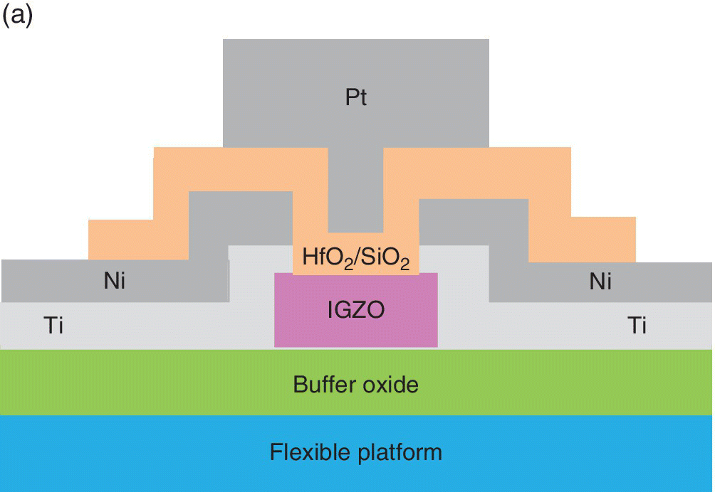

Figure 4.21 Four mask a‐IGZO TFTs with top gate top contact on flexible polyimide substrate in (a) coplanar configuration and (b) staggered configuration.
Based on T.H. Hou et al. (NCTU), AM‐FPD, July 2, 2013 [42].
The staggered a‐IGZO TFT used a reversed patterning sequence for the active regions and the S/D contacts. Also in the staggered TFT, the top gates and S/D contacts were replaced by Ni and Ti respectively. The resistance memory at the drain bit was activated by applying a 4 V forming voltage to the drain with the gate grounded. A stable bipolar resistance was attributed to the connection and rupture of Ni filaments in HfO2 localized at the gate drain overlap region. The logic transistors and resistance memory device had good characteristics in both flat and flexed states, making it potentially for low cost flexible embedded memory applications.
The logic transistors before forming had SS for the coplanar device of 120 mV/decade while the staggered one had SS of 140 mV/decade. Mobility of the coplanar device was 21 cm2/(V s) while the staggered one was 2 cm2/(V s). The forming voltage for the coplanar device was +4 V and for the staggered one was –6.5 V. Reliability characteristics differed only in retention, which was >10 years at 85 °C for the coplanar device and >104 s at 85 °C for the staggered one. The pulse speed was 50 ns for the coplanar and 10 µs for the staggered device.
A three‐state nonvolatile resistive memory for a‐IGZO TFT circuit was discussed in October of 2013 by National Chiao Tung University [43]. A logic compatible flexible amorphous indium–gallium–zinc oxide (a‐IGZO) TFT was made at low temperature. Before electrical forming, the a‐IGZO TFT showed good transistor characteristics such as an ON/OFF current ratio of 8.8 × 10⁶, steep subthreshold slope of 0.14 V/decade, V th of 0.55 V, and maximum field‐effect mobility of 2 cm/(V s). After electrical forming, a three‐bit‐per‐cell resistive switching memory was obtained using localized multilevel resistance states. Good transistor and NVM characteristics were found using a staggered a‐IGZO TFT structure.
The device was made at low temperature on a flexible substrate and offered low cost integration and good characteristics during flexing. This offers the potential for system‐on‐plastic applications. The staggered a‐IGZO TFT was made using the four mask process flow. The three distinct resistance states in the a‐IGZO TFT RRAM memory are illustrated in the I–V curve in Figure 4.22. Voltage was applied to the drain while the gate was grounded. SET pulses were –5 V for 10 µs and RESET pulses were 5 V for 500 µs. Good retention characteristics at 85 °C for the three states were shown to 104 cycles. Bending endurance was good over 104 s with a 10 nm bending radius.
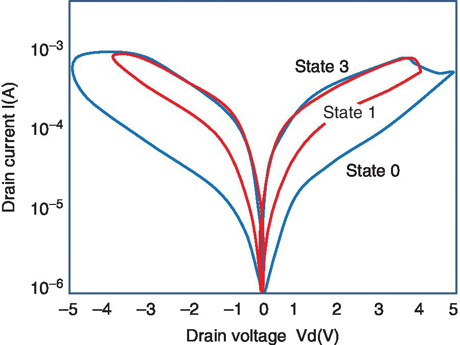
Figure 4.22 I–V curve of a‐IGZO RRAM memory showing three resistance states.
Based on S.C. Wu et al. (NCTU), IEEE Electron Device Letters, 34 (10), October 2013 [43].
In July of 2015, Kyun Hee University discussed the nonvolatile memory performances of transparent flexible thin film memory transistors using IGZO channels and ZnO charge trap layers [44]. An ON/OFF ratio greater than 7 orders of magnitude was found for the fully transparent charge trapping TFTs made on glass substrates when the width of the program pulses were set as 500 nm and the amplitude set at ±20 V. The memory window was 25.8 V wide.
To enable transmittance to visible wavelength, the gate electrodes were made of transparent In–Sn–O layers, which permitted the overall device structure to be made with all‐oxide gate stacks. Memory operations of the flexible charge trap memory TFTs on plastic polyethylene naphthalate substrates were also discussed.
4.4.6 Other Polymer Resistive RAMS with Flexible Substrates
Dynamic response of Al2O3/polymer diode RRAM was discussed in April of 2013 by the Institute de Telecommunications Lisboa, Portugal, who demonstrated dynamic response of a bistable resistive NVM made of Al2O3/polymer diodes [45], These diodes were probed in both the OFF and ON states with triangular and step voltage profiles. The OFF‐state response followed the predictions based on a classical, two‐layer capacitor description. As voltage scan rates increase, the model predicts that the fraction of the applied voltage, V ox, appearing across the oxide would decrease.
Device responses to step voltages in both the OFF and ON states show that switching events are characterized by a delay time. Coupling these delays to the lower values of V ox found during fast scan rates, the observation in the on‐state that device currents decrease with increasing voltage scan rate can be explained. If it is assumed that a critical current is required to turn off a conducting channel in the oxide, then a model can be formulated to explain the shift in the onset of negative differential resistance to lower voltages as the voltage scan rate increases. The fundamental limitations on the speed of operation of a bilayer resistive memory appear to be the time and voltage dependance of the switch‐on mechanism rather than the switch‐off process. This result sheds light on the apparently anomalous behavior of the on‐state, which is the disappearance of the negative differential resistance region at high voltage scan rates.
Resistive switching in multiferroic thin film was discussed in September of 2013 by various Chinese and German labs, which found resistive switching properties in multiferroic BiFeO2 and YMnO3 thin films grown by pulsed laser deposition [46]. Both materials when sandwiched between Au top and Pt/Ti bottom electrodes showed nonvolatile resistive switching when an electric field was applied. BiFeO3 switched in bipolar mode when a positive and negative bias was applied. The resistance ratio between high and low resistance states was larger than 100. The switching mechanism was described by a model of the flexible Schottky‐like barrier at the BFO/Pt interface, which may be related to the drift of oxygen vacancies (ions). An illustration of the bipolar I–V curve of the Au/BiFeO3/Pt/Ti is shown in Figure 4.23.
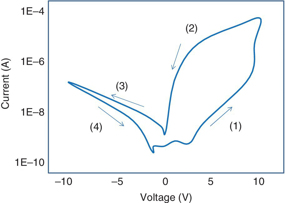
Figure 4.23 Illustration of the bipolar I–V curve of a flexible Au/BiFeO3/Pt/Ti RRAM.
Based on A. Bogusz et al. (Chemnitz Tech, University of ES&T Chengdi, IIN Dresden), ISCDG, September 26, 2013 [46].
YMnO3 showed a unipolar resistive switching with the resistance ratio between the high resistance state and low resistance state greater than 105. In this case the origin of the behavior was thought to be the formation and rupture of conductive filaments. Both of the films were considered potential for future NV RRAMs.
Ag/polystyrene/Ag conductive bridge RAM (CB‐RAM) nanogap devices were discussed in November of 2013 by the University of Pennsylvania [47]. A CB‐RAM was made with silver/polystyrene/silver nanogap devices. This reversible resistive switching used metal filament formation as the switching mechanism. The devices were encapsulated in polystyrene. The switching showed a high ON/OFF current ratio of >103 during cycle switching tests over many cycles. The gap was observed to evolve after extensive testing. Reversible electrical bistability was accomplished with an electrically inactive polymer, which expands the range of polymers suitable for organic digital memory applications.
A switchable diode effect in a polycrystalline thin film BiNdTiO RRAM was discussed in December of 2013 by Xiangtan University [48]. A switchable diode effect with a residual polarization of 55 μC/cm2 was shown in the BiNdTiO RRAM when fabricated on Pt/Ti/SiO2/Si substrates by chemical solution deposition. Consistencies of the P–V and I–V curves showed that the switchable diode effect was primarily caused by polarization modulated Schottky‐like barriers. The ON/OFF current ratio based on these switchable diodes was greater than three orders of magnitude during the retention capacity measurement. The polycrystalline BNT thin films were thought promising for the resistive memory applications.
Resistive switching in Au/pentacene/Si‐nanowire (NW) arrays was discussed in February of 2014 by National Changhua University of Education [49]. Resistive switching memory devices were fabricated including: Au/pentacene/n + Si, Au/pentacene/Si NW and Au/pentacene/H2O2 treated SiNWn + Si. The Au/pentacene/SiNW/n + Si devices showed hysteresis type behavior. H2O2 treatment could potentially lead to degradation of the hysteresis curve. No hysteresis current–voltage characteristics were observed for Au/pentacene/n + Si devices, which may indicate that the resistive switching characteristic is sensitive to silicon nanowire characteristics and that, potentially, the charge trapping effect originates from the SiNWs. The exploration of SiNWs as organic memory devices was thought promising.
Resistive memory based on PEDOT:PSS polymer was discussed in September of 2014 by the Changchun Institute of Applied Chemistry. Resistive memory devices based on PEDOT:PSS doping with polyvinyl alcohol were studied [50]. The resistive switching characteristics of the memory device were found to be dependent on the treatment of the polymer blend film by UV‐ozone. The UV‐ozone treated device showed improved performance. The ON/OFF current ratio was greater than 100. ON and OFF state retention was over 96 hours without deterioration. The resistive switching behavior in the UV‐ozone treated device was attributed to the formation and rupture of PEDOT‐PSS filaments as well as to narrow conducting paths through the native aluminum oxide.
In January of 2016, the University of Rome, Technical University Munchen, CNR‐ISMN, NanoTecCenter Weiz, and Graz University of Technology discussed modeling of filamentary conduction in organic thin film memories [51]. A semiclassical drift‐diffusion model was developed of electrical conductivity in the filament. It was shown that the global behavior of a memory device and the total current can be explained by fully formed and well connected filaments.
Resistive switching has been observed in many organic materials and two main mechanisms have been proposed to explain the bistable behavior. One mechanism is nanoparticles in the material that can act as trap sites. The bistability is an effect of the trapped charge, which can be trapped and detrapped under the control of an applied voltage, thereby switching the device. The other mechanism is the formation of highly conductive localized filaments, which provide pathways for current. These ionic pathways are formed under the influence of an applied voltage. The I–V characteristics of light exposed devices show a different open circuit voltage for each resistive state. This behavior is typical of an organic photovoltaic cell coupled with a shunt resistance, which is the filament.
A heating model of the filament was used to check if assumptions on the number of filaments and their radii were physically plausible. This permits an organic ITO/Alq3/Ag memory device to be pictured as an equivalent circuit under light where the conductive filaments can be represented as a shunt resistance R sh. The total current is I = I org – V/R sh. Different resistive states correspond to different open circuit voltages. The equivalent circuits of an organic ITO/Alq3.Ag RRAM memory device is shown in Figure 4.24. Alq3 is chemically C27H18AlN3O3 and ITO is indium–tin–oxide.
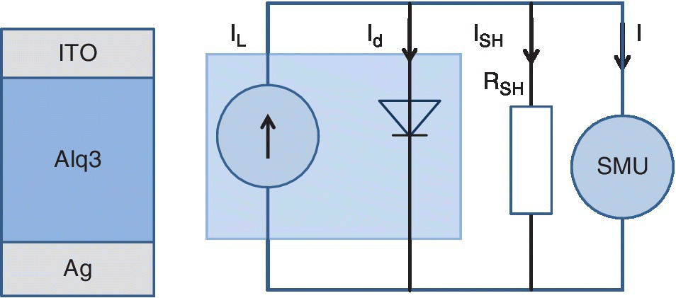
Figure 4.24 Equivalent circuit of an organic ITO/Alq3/Ag Memory Device where Alq3 is chemically C27H18AlN3O3 and ITO is indium–tin oxide.
Based on F. Santoni et al. (University of Rome, TU Munchen, CNR‐ISMN, NTC Weiz, Graz Tech.), IEEE Trans. on Nanotechnology, 15 (1), January 2016 [51] (permission of IEEE).
The ITO is used as an optically transparent bottom electrode. For the photovoltaic measurements, the device was illuminated with an inorganic blue emitting LED driven with a constant current. A symbolic view of the switching process showing the forming process is shown in Figure 4.25 (a). The ON/OFF switch intermediate state is shown in Figure 4.25 (b) and the OFF/ON switch is shown in Figure 4.25 (c).
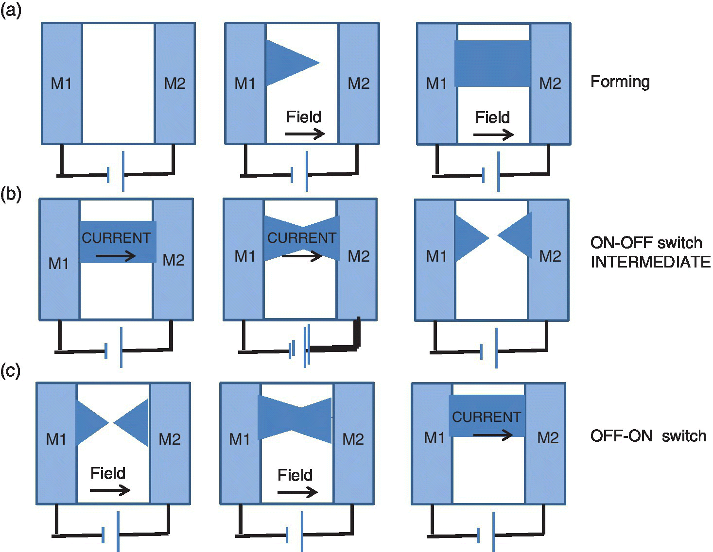
Figure 4.25 Schematic showing the switching process showing: (a) forming, (b) ON/OFF, (c) OFF/ON.
Based on F. Santoni et al. (University of Rome, TU Munchen, CNR‐ISMN, NTC Weiz, Graz Tech.), IEEE Trans. on Nanotechnology, 15 (1), January 2016 [51] (permission of IEEE).
A semiclassical drift‐diffusion model of the electrical conductivity of the filament was developed. The model correctly accounts for the behavior of the device observed by the photovoltaic measurements. Both trap‐assisted Poole‐Frenkel emission and Miller‐Abrahams hopping can be used to explain the observed behaviors. Poole‐Frenkel emission described the motion of electronics in an insulator due to random thermal fluctuations, which provide the energy to move electrons out of a localized state and into the conduction band before falling back into another localized state. The Miller‐Abrahams hopping is based on a phonon‐assisted tunneling mechanism. A simple thermal analysis was used to estimate the number of formed filaments and their radii.
A new type of resistance RAM memory device using graphene oxide (GO) Al/GO‐PEDOT: PSS/Pt was discussed in August of 2016 by Tsinghua, Beijing, and Fuzhou Universities [52]. The RRAM was nonvolatile and bipolar switching. The GO‐PEDOT:PSS composite showed potential for use in high density flexible nonvolatile RRAM memory. It showed repeated high speed switching, 1–3 V tight distribution of HRS and LRS and retention greater than 104 s. The ON/OFF current ratio was about 200.
In August of 2016, Kyong Hee University discussed a multilevel RRAM with a thin‐film transistor (TFT) structure [53]. A three‐terminal device structure was used, resulting in integration of a resistive change memory into the thin film transistor configuration. The three terminals were source (S), drain (D), and top electrode (TE). The device was formed on either a glass or a plastic substrate. Figure 4.26 shows a schematic cross‐section of the three‐terminal resistive change device.

Figure 4.26 Three terminal resistive change devices in TFT configuration with AZO channel.
Based on W.H. Lee et al. (Kyong Hee University), IEEE Electron Device Letters, 37 (8), August 2016.[53].
Both the functions of a transistor and a nonvolatile memory could be performed. Al‐doped ZnO (AZO) was used for the active channel of the TFT and for the resistive change material in the memory device.
The resistive change memory operations in the AZO could be found between the source and drain and the top electrode by the formation and collapse of the conductive filaments. The initial state is from the first forming process at the TE and the S/D regions. The first SET state was programmed by switching events at the TE/source region and the second SET state was programmed by a SET switching events at the TE/drain region. The final RESET state was programmed by the RESET switching event at both regions. The three states consisted of the RESET state, a single source or drain SET state, and a SET state for the source and drain.
The multilevel memory operations were realized by controlling the number of conducting filaments formed in the channel between the source, drain, and the top electrode, which effectively modulated the Ids levels in three different states. The programmed Ids values could be switched in a stable manner among the RESET, a first SET, and a second SET state. There were no variations in the programmed Ids at each memory state during a 10 hour retention time. The programmed current ratios for three‐level memory states were 1:3.8:25. Retention was 104 s and program endurance was 100 cycles.
An illustration of the bipolar resistive switching I–V characteristics of the Al/Al2O3/AZO/ITO structure between the source and drain and the top electrode is shown in Figure 4.27.
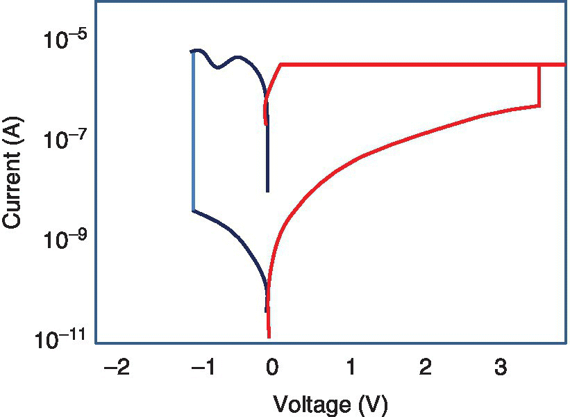
Figure 4.27 Bipolar resistive switching I–V characteristics of Al/Al2O3/AZO/ITO structure between top electrode (TE) and the source (S) and drain (D).
Based on W.H. Lee et al. (Kyong Hee University), IEEE Electron Device Letters, 37 (8), August 2016 [53].
An indium–‐tin‐oxide (ITO) RRAM with an ultralow switching voltage due to an inserted SiO2 layer was discussed in October of 2016 by National Sun Yat‐Sen University, University of Texas, Austin, National Cheng Kung, University, National Kaohsiung Normal University, and Xiamen University [54]. The amplitude of the switching voltage of the device was below 0.2 V whether measured by direct or by alternating current sweep operation. The observed RESET voltage increased with temperature while the Set voltage did not notably change under temperature variation. To determine the switching mechanism, conduction current fitting and switching voltage statistics were applied to explore the regular voltage variation dependence on temperature.
The switching mechanism of the device was discussed along with the current conduction mechanism. An ohmic conduction mechanism was found to be caused by original carriers at a low electric field. As the operating voltage became larger, the current conduction in the LRS was dominated by hopping conduction. A reaction model was proposed to explain the oxygen concentration gradient induced between the inserted SiO2 and the ITO electrode on the ITO‐based RRAM device.
Inkjet printed high performance RRAMs based on a high‐k HfO2 dielectric were implemented in April of 2017 by the Universities de Barcelona and Autonoma de Barcelona [55]. The technology had a high ON/OFF current ratio and low switching voltage, which could permit low power applications. The inkjet printed dielectric layer resulted in a flexible substrate that could enable low integration density memory in portable devices. The simple vertical metal–insulator–metal structure of the RRAM appeared suitable to this application. The use of a crossbar architecture permitted scalability.
Inkjet printing permitted a versatile, maskless, noncontact digital fabrication method that could be done at ambient room conditions. One memory cell that was found flexible and inexpensive was Cu/Cu x O/Ag for working at low voltages, but lack of resolution and of available inks were drawbacks. The study focused on inkjet printed HfO2 as a flexible thin film dielectric layer for an HfO2 based RRAM device. Inkjet printed RRAMS were shown to have comparable features to conventional CMOS compatible RRAMs.
An illustration of an RRAM with Ag top contact, HfO2 dielectric, and Au bottom contact is shown in Figure 4.28. The device is about 1 mm square. The Au bottom electrode is 50 nm thick, HfO2 was 200 nm thick, and the Ag top electrode was 700 nm thick.
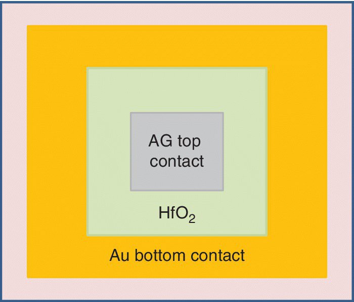
Figure 4.28 Illustration of 1 mm2 HfO2‐based RRAM with 50 nm thick Au BED, 200 nm thick HfO2 dielectric, and 700 nm thick Ag top electrode.
Based on G. Vescio et al. (University de Barcelona, University A. de Barcelona), IEEE Electron Device Letters, 38 (4), April 2017 [55].
An HfO2 nanoparticle ink was printed over the bottom electrode while the substrate temperature was kept at a constant 30 °C. A 3 hour postdeposition annealing process at 240 °C in a vacuum was needed to eliminate the solvents. A 700 nm thick silver top electrode was printed on the dielectric followed by annealing in vacuum at 200 °C to remove organic solvents and attain resistivity of about 16 µohm cm. A minimum thickness for each printed layer was specified to avoid pinholes. A forming process with current limitation was used to create a switchable conductive filament. A bipolar resistive switching process was used with positive bias for SET and negative bias for RESET. The I on/I off ratio was around 1000 in most cycles.
In May of 2017, National Cheng‐Kung University, National University of Kaohsiung, and Air Force Institute of Technology, Kaohsiung, discussed the performance of flexible RRAM devices based on simple spin‐coated sol gel derived strontium titanate nickelate (STN) thin films on a polymer substrate [56]. The stack of the device is shown in Figure 4.29. These devices had an ON/OFF current ratio of 105 and showed a uniform current distribution.
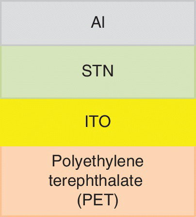
Figure 4.29 Stack of flexible RRAM devices based on simple spin‐coated Sol Gel derived strontium titanate nickelate thin film on polymer substrate.
Based on K.J. Lee et al. (NCKU, NU and Air Force IT, Kaohsiumg), IEEE Trans. on Electron Devices, 64 (5), May 2017 [56].
Issues with metal oxide‐based thin film RRAMs include: a low ON/OFF ratio (<103), cracking issues during repeated bending, and poor current distribution. The stability of the STN thin film is in part due to the strong bonding between bidentate ligands of nickel acetylacetone and titanium metal ions, which enable the chelation effect. The Ni ions can act as clusters and play a critical role in the formation and rupture of cone‐shaped conductive paths during resistive switching. The formation and rupture process promotes local alignment of oxygen vacancies among metallic Ni clusters, which enhance the distribution of switching parameters. Figure 4.30 illustrates the resistive switching mechanism of the STN‐based RRAM in the (a) pristine, (b) LRS, and (c) HRS conditions. The devices were made on a flexible plastic substrate and were durable under a repeated bending test.
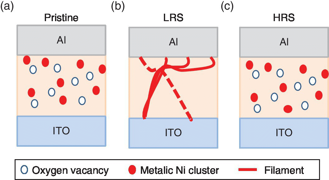
Figure 4.30 Illustration of the resistive switching mechanism model of the STN‐based RRAM in the (a) pristine, (b) LRS, and (c) HRS conditions.
Based on K.J. Lee et al. (NCKU, NU and Air Force IT, Kaohsiumg), IEEE Trans. on Electron Devices, 64 (5), May 2017 [56].
It was found that the STN thin film prepared by a solution process could be used effectively in making flexible memory devices with forming‐free resistive switching. The ON/OFF ratio was 105 after 90 days under an atmospheric environment. Current distribution showed good uniformity. The ON/OFF ratio showed no obvious degradation after 100 bending cycles. An increased barrier height, after adding the Ni, meant a lower HRS current and higher ON/OFF ratio. The metallic Ni clusters were used to interpret the switching mechanism in the STN devices.
In May of 2017, the Imperial College London and King Abdullah University of S&T discussed resistive switching memories based on empty aluminum nanogap electrodes [57]. Adhesion lithography was used to make the dense arrays of RRAMs along with a low temperature, large‐area‐compatible nanogap fabrication technique. These arrays were made on both rigid and flexible plastic substrates. The devices showed a nonvolatile memory operation. Endurance was stable. Resistance ratios were >104 and retention time was several months. The controlled resistive switching was found to be due to migration of metal from the electrodes into the nanogap when an external electric field was applied. This technology had potential in large area electronics and also in electronics for harsh environments such as: space, high and low temperatures, radiation, vibration, and pressure.
4.5 Charge Trapping Nanoparticle (NP) Memory on Flexible Substrates
4.5.1 Overview of Charge Trapping NP Memory on Flexible Substrates
A polymer carbon nanotube charge trapping memory was made using a thin parylene layer separating an SiO2/nanotube interface from the polymer coating. Graphene nanocrystal (NC) memory in a polymer matrix was studied where the graphene quantum dots acted as charge traps.
Inkjet printed IGZO thin film transistors with nanoparticle storage was described. Al/Au nanoparticles embedded in polystyrene were made with a good memory window for multilevel operation. RRAMs with NC of different diameters were found to suppress switching fluctuations. Variation of the resistive switching parameters for NP memories was studied.
4.5.2 Carbon Nanotube Charge Trapping Memory with Flexible Substrates
Polymer carbon nanotube (CNT) charge trapping memory was discussed in January of 2013 by CEA, IRAMIS, CNRS, and LEM. These devices were used as optoelectronic nonvolatile memories [58]. The detailed mechanism of charge trapping of mixed organic/inorganic optoelectronic devices was investigated by intercollating layers of parylene at different interfaces in the device structure. A thin parylene layer separated the SiO2/nanotube interface from the photosensitive polymer coating. The structure was suggested as an optimized solution for charging, stability, and robustness. A schematic cross‐section of this structure is shown in Figure 4.31.
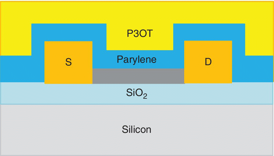
Figure 4.31 Schematic of a polymer carbon nanotube charge trapping memory using a thin parylene layer separating the SiO2/nanotube interface from a photosentive polymer coating.
Based on B. Brunel et al. (CEA, IRAMIS, CNRS, LEM), Applied Physics Letters, 102 (1), 013103, January 2013 [58].
To be used in reconfigurable circuits, the memory devices must support multiple reprogramming and read cycles. The robustness of the geometry was verified by performing more than 200 cycles. The ON/OFF ratio remained approximately constant while the ON and OFF states showed some variability. The metallic CNTs were suboptimal but it was expected that single tube devices would not have an issue.
Memory properties of graphene quantum dots in semiconducting poly93‐hexlthiophene polymeric matrix were discussed in August of 2014 by the National Institute for R&D in Microtechnology, Romania [59]. These graphene quantum dots act as charge trapping particles. The I–V measurements of thin films made from this nanocomposite deposited on gold interdigitated electrodes indicated that the whole transport I–V characteristics showed a strong nonlinear behavior and a hysteresis curve representative of a memristive response.
In November of 2015, Fuzhou University and Hanyang University discussed a solution involving processed, flexible, transparent nonvolatile memory with embedded graphene quantum dots in polymethylsilsesquioxane layers made on a transparent flexible substrate [60]. The hysteresis window was found from the current–voltage plots. The nonvolatile memory devices were reprogrammable and stable up to 1 × 10⁴ s with an ON/OFF current ratio of 104. The memory showed a stable hysteresis window with no obvious degradation upon bending under different radii of curvature.
Graphene quantum dots were used as the charge trap medium due to properties such as chemical inertness, low toxicity, and higher work function than other reported nanoparticles. The quantum confinement effect and boundary effect also made them a good charge trapping medium. Two MIMs were used. The structures were: MIMA Ag NW/PMSSQ/indium–tin oxide and MIMb Ag NWPMSSQ/GQD/PMSSQITOPET. The I–V characteristics of MIM‐B on a semilog scale are indicated in Figure 4.32. A representative hysteresis curve is shown.
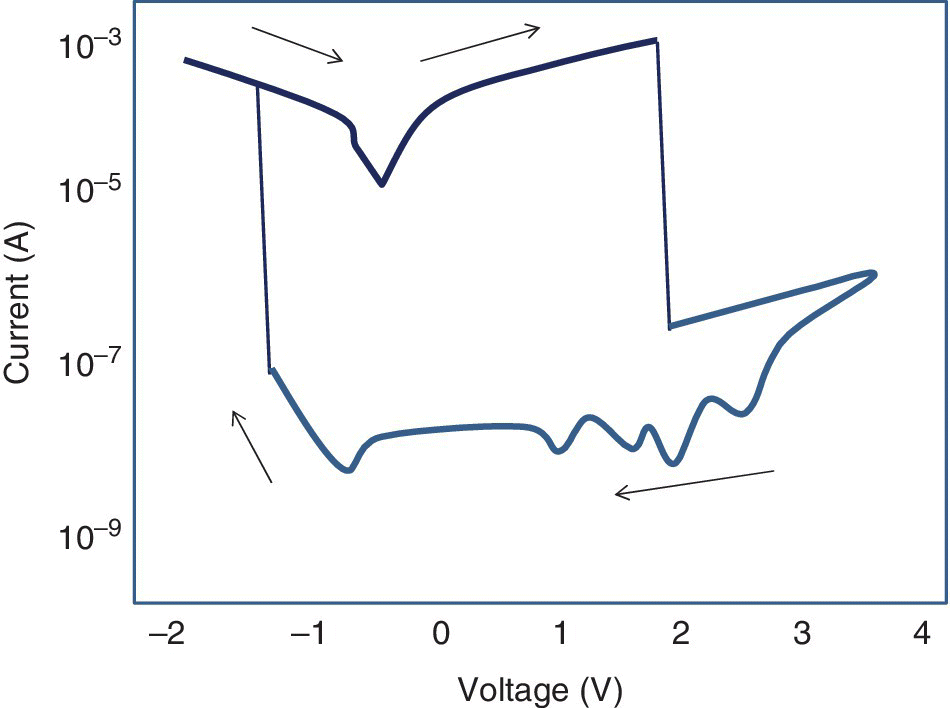
Figure 4.32 I–V switching characteristics on a semilog scale showing hysteresis curve of MIMb consisting of Ag NWPMSSQ/GQD/PMSSQITOPET.
Based on J. Lin et al. (Fuzhou University, Hanyang University), IEEE Electron Device Letters, 36 (11), November 2015 [60].
An illustration of the band diagrams for the (a) write process and the (b) erase process are shown in Figure 4.33. The device was programmed when electrons were trapped in the graphene quantum dots and erased when the electrons in the GQDs were detrapped.
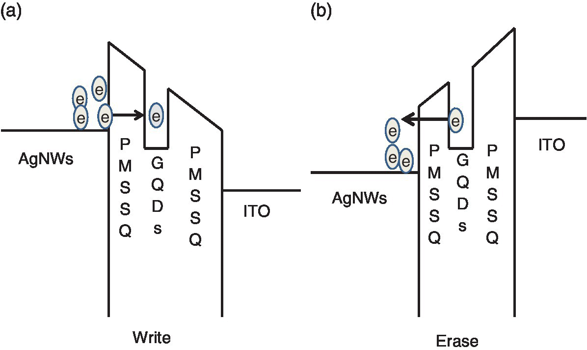
Figure 4.33 Band diagrams for (a) the write and (b) erase processes.
Based on J. Lin et al. (Fuzhou University, Hanyang University), IEEE Electron Device Letters, 36 (11), November 2015 [60].
4.5.3 Inkjet Printed Nanoparticle Memory
An inkjet printed thin film transistor (TFT) with silicon NP storage was discussed in January of 2013 by the Technical University of Singapore. An NP memory was produced with an inkjet printed In–Ga–Zn oxide (IGZO) thin film transistor [61]. An SiO2 gate dielectric was used that had embedded silicon nanoparticles (SiNP). The SiNP acted as charge trapping sites. A clockwise V gs–I d hysteresis curve was found. The curve was attributed to the charging and discharging of the silicon nanoparticles. The printed IGZO‐based memory had an ON/OFF current ratio of 103.
4.5.4 Other Nanoparticle Charge Trapping Memories on Flexible Substrates
Operation of Al/Au nanoparticles in a polystyrene layer was discussed in January of 2014 by Hanyang University, who discussed capacitance–voltage curves for Al/Au nanoparticles embedded in polystyrene layer/p‐Si devices at 300 K [62]. These curves showed a metal–insulator–semiconductor (MIS) behavior with flat‐band voltage shifts of the C–V curves due to the presence of charge trapping. Memory windows between 2.6 and 9.9 V were observed at different voltages, which indicated the potential for multilevel behavior.
Ct measurement showed that the charge trapping capability of Au nanoparticles embedded in a polystyrene layer was maintained for retention times larger than 104 s without major degradation. The multilevel charging and discharging mechanisms were models using the experimental results.
In September of 2015, the National Technical University of Athens discussed resistive switching characteristics of TiN/Ti/TiO2‐x /Au RRAM devices containing Pt nanoparticles (NP) with different diameters [63]. A primary concern was suppressing the fluctuation of switching parameters in the RRAM devices. Since the resistive switching effect originates in the creation and annihilation of conducting filaments within the metal oxide layer, the variations of the switching characteristics would be expected to be due to the stochastic nature of the conductive filament formation. While it is difficult to control the complex dielectric breakdown process, it is simple to indicate the regions in which it occurs. A significant improvement in switching parameters resulted from embedding metal nanoparticles in the dielectric matrix. This study looked at the influence of Pt NP size and density on the resistive switching properties of room temperature deposited TiO2 thin films. These operate without an electroforming process and showed large switching ratios. It was found that the devices with Pt NC embedded had improved uniformity and reliability as well as multilevel capability from increasing the NC size. Pt NCs assisted the formation of oxygen vacancy‐based filaments near the location of the NCs. This is important for increased uniformity since it limits the creation of clustered oxygen vacancy regions that show uncontrolled switching patterns.
Physical vapor deposition (PVD) was used with the process integrated in a single vacuum system. This permitted formation of a metal oxide thin film with embedded nanocrystals made under high purity vacuum conditions.
The RRAM device structure was: TiN/Ti/TiO2/Pt NCs/TiO2/Au/SiO2/Si. The MIM capacitors were patterned using lift‐off lithography. Each square electrode was about 100 × 100 µm2. Electrical characterization was done by applying all signals to the top electrode while keeping the bottom electrode grounded.
A typical DC current–voltage hysteresis loop for an RRAM is shown in Figure 4.34. The solid line represents the RRAM with 3 nm Pt NP and the black dotted line indicates the RRAM without the NP. The continuous transition between the HRS forward sweep and the LRS backward sweep is indicated. The arrows indicate the switching direction. The sweep is from –4 to +4 V.

Figure 4.34 Typical DC current–voltage hysteresis loop for a TiN/Ti/TiO2‐x/Au RRAM device (a) with 3 nm Pt NP (solid line) and (b) without NP (dotted line).
Based on P. Bousoulas et al. (NTU Athens), ESSDIRC, September 2015 [63].
A significant improvement of the resistive switching parameters was attained by embedding Pt NPs of different sizes and densities in the dielectric matrix. Variability was reduced by the enforcement of the possible percolative networks where switching took place. The bigger NPs induce very large ON currents with 3 nm Pt NP considered the optimum solution for spatial variability and power consumption. The small size of the NP permits integration into thin dielectric films, permitting device scaling. Multilevel capabilities were demonstrated.
Transparent memories using nanoparticles (NP) of polymer/ZnO nanocomposites were discussed in February of 2016 by National Taiwan University, National Taipei University of Technology, and National Central University [64]. These floating gate memories with metal NP covered with insulating polymer are studied for next generation nonvolatile organic memory. At issue is the fact that the transparency of the device with metal NPs is restricted to 60–70% due to the light absorption in the visible region caused by surface plasmon resonance effects of the NPs. A new memory used blends of hole trapping poly(9‐(4‐vinylphenyl) carbazole) with electron trapping ZnO NPs for charge storage. The memory stack is shown in Figure 4.35.

Figure 4.35 Transparent memory stack with polymer/ZnO nanoparticles for storage.
Based on C.C. Shih et al. (National Sun Yat Sen University), Scientific Reports, February 1, 2016 [64].
These devices showed a programmable memory window of 60 V during program/erase due to trapping and detrapping of charge carriers in the ZnO NP/PVPK composite. The retention time was >105 s and endurance was greater than 200 cycles. The devices had a transparency of 90% at 500 nm wavelength for the spray‐coated PEDOT:PSS electrode.
Flexible thin film transistors using the IGZO channel and ZnO charge‐trap layers made on polyethylene naphthalate (PEN) substrate were discussed in April of 2016 by Kyung Hee University and the Electronics and Telecomm Research Institute [65]. The fabrication process temperature was below 180 °C. An organic/inorganic hybrid barrier layer was introduced to improve the surface roughness and water vapor transmission rate of the PEN substrate. The gate stack was all oxide layers with an InGaZnO (IGZO) active channel, ZnO charge‐trap layer, Al2O3 blocking/tunneling layers, and In–Sn–O (ITO) transparent electrode in which the double layer tunneling and top protection layers were designed. A wide memory margin of 25.6 V, fast programming speed of 500 ns, and retention time of greater than 3 hours were achieved at 25 °C and at 80 °C. These memory characteristics were not degraded after delamination of the PEN substrate or under bending with a radius of curvature of 3.3 mm.
The switching behavior of TaN/Al2O3:Ag:ZnO/ITO resistive RAMs made on flexible substrates using embedded Ag nanoparticles was discussed by Fudan University in July of 2016 [66]. Variation in the resistive switching parameters is a critical issue in RRAMs. The embedded Ag nanoparticles improved device yield and reduced resistance variability from more than 160% to 30%. The Ag NP also reduced variability in SET voltages from 35 to 18% and in RESET voltages from 40 to 11%. Synaptic behavior of this flexible device was shown opening potential applications in neuromorphic computing applications.
The RRAM devices were made on flexible substrates. A 10 nm thick ZnO film was deposited on an ITO‐coated PET substrate using atomic layer deposition (ALD) at 130 °C with various precursors. The Ag nanoparticles were spin‐coated on the ZnO layer and baked at 100 °C to evaporate the solvent. Then a 10 nm Al2O3 layer was deposited using ALD at 130 °C with precursors. A 50 µm2 top electrode was defined using photolithography followed by a PVD deposited layer of TaN followed by a lift‐off process. The effect of the nanoparticles can be seen in the bipolar switching I–V curves of the TaN/Al2O3:Ag:ZnO/ITC RRAM devices (a) with and (b) without the nanoparticles in Figure 4.36. The average surface density of the Ag nanoparticles was estimated at 1.3 × 10⁸/cm2.
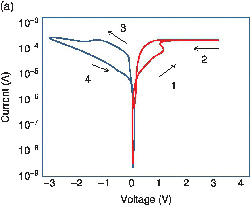
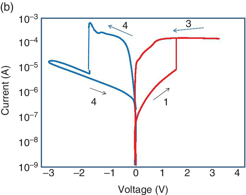
Figure 4.36 Illustrations of I–V curves of (a) TaN/Al2O3:Ag:ZnO/ITO RRAM devices with Ag nanoparticles (NP) and of I–V curves of (b) TaN/Al2O3/ZnO/ITO RRAM devices without Ag NP.
Based on D.T. Wang et al. (Fudan University), IEEE Electron Device Letters, 37 (7), July 2016 [66].
The reset current of the sample with the Ag NPs is smaller than that without the NPs. The set and reset processes were abrupt without the Ag NP, while with the Ag NP gradual set and reset processes were found. The retention after folding the material hundreds of times showed only a slight shift after 104 s. The 10 year memory window was still good. For the set process the switching speed of the Ag NP embedded device reached 100 ns while the control device was 10 ns. For reset, the switching speed with the Ag NP reached 1 µs and without the Ag NP was 10 ns. This was attributed to the slower speed of Ag ions compared to oxygen vacancies. The device with Ag NP showed gradual set and reset processes. The Ag NPs enhanced the device yield and uniformity, lowered the operating voltage, and reduced power consumption. This improvement was attributed to Ag ions providing an easy and controllable path to the formation of a conductive filament and suppressing random filament formation and rupture.
In September of 2016, KAIST discussed a floating gate memory using an MoS2 channel with a metal nanoparticle charge trapping layer and polymer tunneling dielectric [67]. MoS2 is a 2D planar material, like graphene, which has a layer dependent bandgap from 1.4 to 1.8 eV with high mobility of about 150 cm2/(V s) and a high ON/OFF current ratio of 109. The device has a Ti/Au source and drain, 90 nm SiO2 dielectric, and heavily p‐doped bottom gate. A schematic cross‐section of the device is shown in Figure 4.37.

Figure 4.37 Schematic cross‐section of a floating gate memory with an MoS2 channel with an Au nanoparticle charge trapping layer.
Based on M.H. Woo et al. (KAIST), ESSDERC, September 2016 [67].
For fabrication, a conformal, stable polymer insulator layer was deposited via initiated chemical vapor deposition (iCVD), which ensured the memory could endure a significant electrical stress. Different thicknesses of gold nanoparticles, achieved by means of thermal evaporation, were used to control the density and distribution of nanoparticles in the charge trapping layer, while the Al2O3 blocking dielectric was deposited using an atomic layer deposition (ALD) process to increase the gate coupling ratio for low power operation. The floating gate memory device was fabricated and showed a tunable memory window with a high ON/OFF ratio after applied programming and erase pulse. This permitted multibit data storage with a long retention current ratio (I on/I off).
The trap and detrap of charges from the MoS2 channel to the gold NP layer determined the program and erase states during memory operation. The ON/OFF ratio was greater than 108 and the mobility was 18.6 cm2/(V s). The device showed a stable memory operation with a 6.8 V memory window and more than 103 s of data retention with greater than 103 current ratio.
4.6 Transfer of Conventional Memory Chips on to Flexible Substrates
Flexible electronics is important for IoT applications due to its low weight, high portability, low fragility, and options for variable structure. Flexible processors and memories are also important for data storage and processing and network communications. For these applications the flexible devices developed using organic and polymeric materials frequently have insufficient performance and low integration density. For these high performance applications, flexible electronics using single substrate integration of silicon electronics devices is needed. Several techniques have been developed for integration of silicon chips on flexible substrates. These are outlined in this section.
4.6.1 Transfer of Silicon Chips Using SOI Base Wafers
Using SOI wafers to create thin layers of memory chips has the advantage of having a thin film of single crystalline silicon, which is compatible with full CMOS. The underlying buried oxide (BOX) layer can be etched away leaving the ultrathin silicon layer or maintained to protect the silicon.
High performance gate‐all‐around (GAA) Si nanowire (NW) SONOS on plastic substrate was discussed in December of 2014 by KAIST [68]. The ultrathin film of single crystal Si‐NW GAA SONOS memory devices were transferred on to a plastic substrate from a host silicon wafer. A schematic representation of the wafer thinning and transfer process is shown in Figure 4.38.

Figure 4.38 Schematic representation of the wafer thinning and transfer process.
Based on J.M. Choi et al. (KAIST), IEDM, December 2014 [68].
The process uses (a) a GAA NW SONOS silicon‐on‐insulator (SOI) over a buried oxide (BOX) and silicon handle wafer; then (b) a protection layer coating and thermal release tape is bonded on, (c) the wafer is then thinned down to the buried oxide, and (d) transferred on to a plastic/polyimide tape; (e) the thermal release tape and protection layer is then removed ending with (f) a GAA Si‐NW SONOS memory device on a flexible plastic substrate. This device can be tested and packaged. The final film layer is about 1 µm thick and the polyimide flexible backing is about 35 µm thick.
To form the GAA SONOS FETs, an SOI wafer with top silicon thickness of 110 nm was used. The top silicon was thinned to 50 nm by oxidation and etch and patterned to form a 50 nm diameter SiNW. The SiNW was reduced to 30 nm by sacrificial oxidation. The NW was suspended by wet etching the buried oxide beneath it while supported at the ends to the source and drain probe pads. The ONO layer was formed with thicknesses of 3/7/12 nm and implantation of source and drain done. SiO2 passivation was deposited and via holes cut, followed by Al deposition and patterning. No device degradation was observed during the film transfer.
There was negligible degradation when the substrate was flexed. Typical I–V curves were found. Program time was 10 ms and erase time 100 ms. The V th window was about 4 V at V prm = 14 V and V ers = –14 V. The result was a high performance nonvolatile memory chip on a flexible polymer substrate.
In December of 2015, KAIST discussed an ultrathin Si‐based flexible NAND Flash memory made without using a conventional transfer process [69]. The device and the flexible substrate are interconnected by flip‐chip thermocompression bonding with anisotropic conductive film (ACF). The bottom sacrificial silicon of the SOI wafer was gently etched away, which left flip‐chip bonded devices, which were sufficiently thinned to roughly 1 µm to make a very flexible fully packaged NAND Flash memory without cracks or wrinkles.
Using SOI wafers to create flexible memory chips has the advantage of having a piece of single crystalline silicon that is compatible with full CMOS. Other advantages are: that an ultrathin chip is known to be highly flexible, which makes the chip resilient under various stress conditions, it provides a direct interconnection between the device and the outer electrode without requiring an additional wiring process, and it is unnecessary to transfer the device to a flexible substrate since the flip‐chip bonded device is already attached to the flexible printed circuit board substrate.
Retention characteristics of the flexible Flash memory showed that the threshold window exceeded 104 seconds. Endurance of more than 2000 program/erase cycles was shown. The I–V curves of the programmed and erased states of a cell in the NAND Flash memory measured at V d = 0.5 V is shown in Figure 4.39. Programming was at V = 12 V and erase at V = –16 V.
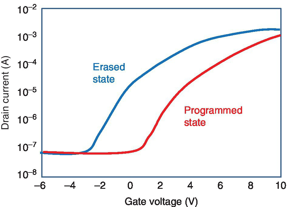
Figure 4.39 I–V curves of programmed and erased states of a cell in the flexible NAND Flash.
Based on D.H. Kim, et al. (KAIST), IEEE IEDM, December 2015 [69].
The final device had reproducible memory operation with good mechanical stability on a flexible substrate. Addressing tests were performed successfully under various conditions. A roll‐to‐roll process was in development to permit mass production of packaged silicon circuits on flexible substrates.
4.6.2 Creating Thin Chips Using an Underlying Cavity
An additive technique for growing ultrathin silicon chips was discussed in February of 2013 by the Institut für Mikroelecktronik, Stuttgart [70]. This method involved growing layers of crystalline silicon one at a time on a foundation laced with sealed cavities. This resulted in the crystalline silicon layer being attached to an array of small vertical pillars, ensuring that the foundation would be strong enough to support the chip throughout the processing but weak enough to snap the finished chip off the top of the wafer. The wafer could then be polished and reused as a substrate.
The process involved etching a 1 µm layer of porous silicon into a solid wafer and then a second, 200 nanometer, layer of more coarsely porous silicon beneath that. Both layers were then sintered at high temperature causing the nanopores in the coarse layer to merge into larger pores. The result was one continuous cavity interrupted by vertical pillars. The surface layer then serves as a seed for the crystalline silicon, which is grown over the entire surface of the wafer to the desired thickness. The chip then goes through typical integrated circuit processing. After fabrication is complete, the surface layer is still firmly attached to the thick silicon wafer by the array of pillars within the buried cavity. A deep trench is then etched at the edges of the chip and down into the cavity, which leaves the chip supported by the pillars alone. A pick‐and‐place tool using a vacuum gripper is used to grab the chip and tug it, snapping the vertical pillars with mechanical force. The tool then places each chip on to a stack or on to a flexible substrate with other thin film components.
In February of 2016, Arizona State University discussed the systematic design of a flexible system [71]. Hybrid flexible systems and system‐on‐polymer (SoP) are described that combine the advantages of flexible electronics and traditional silicon technology. Flexibility of the chip is considered as a new design metric along with power, performance, and area metrics. A new approach to optimization of placement of rigid components on to a flexible substrate is discussed, which can result in minimizing the loss in flexibility.
Flexible electronics include: mechanically bendable, rollable, conformal, or elastic circuits. Flexible electronics are lighter, thinner, and cost less to make. They can be used in wearable systems as part of clothing or labels. Flexible electronics have already been used in displays, sensors, photovoltaic cells, batteries, and small MCU and RF transmitters. Drawbacks of flexible electronics include: lower degrees of integration and performance and larger variations than in current silicon technology. The solution proposed is a form of hybrid flexible electronics where silicon integrated circuits are combined with flexible substrates. These hybrid devices are designated systems on polymer/plastic/paper (SoP) and flexibility is proposed as a new design metric along with usual performance and area metrics.
In June of 2017, The University of Oulu, Meyer Burger BV, and Tampere University discussed using inkjet printed silver traces and interconnections made with the print‐on‐slope technique for connection to an RFID chip operating in the ultrahigh frequency range [72]. An underfill material was used to attach silicon RFID chips on to the flexible polymer substrates. The cured underfill was also used as a sloped surface for printing interconnection traces from the chip to the plastic substrate’s radiators. A single phase continuous roll‐to‐roll compatible process was used. The compatibility of various low temperature nanoparticle inks was tested with different substrate materials. The structures were exposed to thermal/humidity tests at 85 °C/85% relative humidity for up to a 2000 hour period. The samples were characterized by a read range measurement device and by optical imaging and field emission scanning electron microscopy. The bulk conductive traces were characterized electrically by measuring their resistances. The conclusion was that inkjet printing is feasible for producing conductive traces for RFID structures and the print‐on‐slope technique is a cost‐effective method for making interconnections between chip and substrate.
Modeling devices and circuits on flexible ultrathin chips were discussed in February of 2017 by the University of Glasgow [73]. Compact models are needed for simulation and prediction of changes in response to device and circuit bending induced stress to make designing circuits for bendable electronics easier. Compressive and tensile stress studies were done on transistors and simple circuits like inverters with different channel orientation of transistors on ultrathin chips. Two fabricated chips were thinned to 20 µm using conventional dicing‐before‐grinding steps of CMOS processing to obtain sufficient bendability, which was defined as a 20 mm bending radius. Electrical characterization was done of the thinned chip on a flexible substrate. The results showed a change of carrier mobilities in various transistors and threshold voltage of the inverters during different bending conditions. A compact model was developed that predicts the mobility variation, and threshold voltage in compressive and tensile bending stress conditions and orientations. The predictions agreed with the experimental measurements.
4.6.3 Fan‐Out Wafer Level Packaging for Assembling Silicon Chips on Flexible Substrate
Fan‐out wafer level packaging (FO‐WLP) technology extends conventional WLP to provide a greater number of external package contacts while permitting a smaller chip area. The goal is to avoid using expensive silicon for accommodating more I/Os by embedding an individual die in an epoxy‐like material that extends the dimensions of the package beyond the silicon die.
The interconnects are redistributed over the base of the extended package, as shown in Figure 4.40. Figure 4.40 (a) illustrates a single layer of redistribution while Figure 4.40 (b) illustrates a two‐layer redistribution.

Figure 4.40 Redistribution of interconnects over base of extended fan‐out WL package: (a) single layer of redistribution and (b) two layers of redistribution.
In March of 2017, Sumitomo Bakelite Co. discussed the different types of packaging structures found in more advanced wafer level packaging (WLP) [74]. Advanced FO‐WLP is made in a package‐on‐package (PoP) or single inline package (SiP) with multiple side‐by‐side chips. An illustration is shown in Figure 4.41 (a) of fan‐out PoP and in Figure 4.41 (b) of fan‐out SiP with multiple side‐by‐side chips.

Figure 4.41 Advanced fan‐out–wafer level packaging (FO‐WLP) in (a) fan‐out package‐on‐package (FO‐PoP) and (b) fan‐out single‐in‐line package (FO‐SiP).
Based on I. Watanabe et al. (CSTIC), March 12, 2017 [74].
Some changes of process and package structure are required for use of FO‐WLP with epoxy molding compound. For fan‐out PoP a grinding process is required to expose the face of the Cu pillar on the chip. If the die top thickness is below 70 µm, thicker epoxy molding compound is required to control the optical transparency. An application mentioned is a smartphone with an application processor that includes an FO‐WLP as a bottom package in PoP.
In June of 2017, Orbotech discussed an overview of the fan‐out wafer level packaging process and its challenges [75]. An illustration of the process is shown in Figure 4.42.
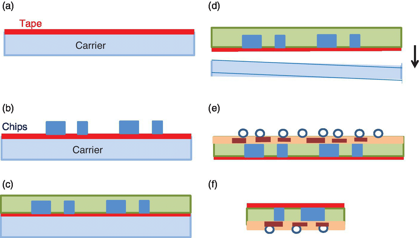
Figure 4.42 Fan‐out wafer level packaging process: (a) application of tape, (b) chip placement, (c) wafer level molding, (d) release from carrier, (e) redistribution and bumping, and (f) singulation.
Based on SPTS Technology Press Release, August 2016 [75].
The chips are initially placed on a tape‐plus‐carrier using a placement tool and then the chips are embedded in a mold compound. The cured mold with the embedded chips is released from the carrier. Redistribution layers for the I/Os are formed and bump processing is done. The individual chips are then singulated.
The FO‐WLP devices can have thousands of I/O points that are seamlessly connected using finely spaced lines as thin as 2 to 5 µm. Heterogenous devices including different types of chips can be included on the substrate and the system connected in the redistribution layers.
Fan‐out wafers feature singulated chips embedded in the epoxy molding compound. Spin‐on dielectrics surround the redistribution layers. Advantages include significant package height reduction by elimination of the substrate. Issues include: moisture absorption, outgassing, and limited tolerance to elevated temperatures. While silicon circuits can withstand heat up to 400 °C and can be degassed quickly, the EMC and dielectrics used in FO‐WLP withstand heat up to about 120 °C and degassing takes longer, which reduces the throughput of a conventional sputter system. Multiwafer degas has helped.
In 2015, TSMC discussed probing for the integrated fan‐out wafer level chip scale package (FO‐WLP) [76]. This package is more cost effective than other current 3D IC packages for consumer mobile wearable and IoT markets. A study was undertaken to improve the quality, yield, and cost of the integrated FO‐WLP by probing copper pillars without solder caps. Adaptive probing was developed to improve traditional fixed probe methods so variations of copper pillar, wafer warping, and noncoplanarity of high pin count probes could be tolerated.
The proposed adaptive probing technique can handle varieties of critical probing cases. Adaptive and online tuning for each die are required. Additional probing depth was used based on the depth of the first passed die using a manual trial. Multiple touchdowns on each die are used in probing to be sure the CuO has been penetrated to reduce the electrical resistance. An adaptive programing algorithm was generated. An example of the concept of adaptive probing is shown in Figure 4.43.

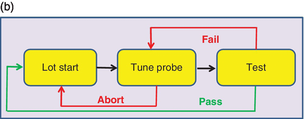
Figure 4.43 Concept of adaptive probing: (a) traditional fixed probing and (b) adaptive probing with probing depth set according to initial test results.
Based on M. Lee et al. (TSMC), eMDC&ISSM, September 2015 [76].
In 2016 Kulicke and Soffa Industries discussed thermocompression bonding for FO‐WLP using new equipment with much higher throughput than before, which significantly lowered cost per unit [77]. This equipment was developed to support next generation fine pitch, 2.5D and 3D assemblies using Cu interconnects. It was adapted to support die placement for fan‐out wafer level packaging (FO‐WLP) and also for high accuracy flip‐chip placement. Although there was initial concern about the differential cost of the process compared to an earlier process, as the units per hour approached 1400, the difference became negligible.
The first assembly step in an FO‐WLP process is the placement of known good die on to a carrier. These dies can be either face up or face down. In single die face down FO‐WLP packages placement accuracy is important but not critical and the required resolution for redistribution layers is typically 10 µm. In more advanced multidie SiP FO‐WLP products, the requirement is 5 µm or less and die placement accuracy becomes critical for assembly yield. Underfills applied prior to bonding can be a nonconductive paste (NCP) or a nonconductive film (NCF) that is applied to the wafer prior to dicing. High volume NCF processes are expected to dominate production as the units‐per‐hour rate increases.
Several fatigue‐related mechanisms connected to standalone package reliability or solder joint capability have been investigated successfully for FO‐WLP. In 2017, MediaTek discussed a failure mechanism induced by chip‐to‐board interaction for FO‐WLP [78]. This is a failure mechanism specifically related to this packaging technology. Circular cracks were detected on passivation and on the redistribution layer (RDL) due to mismatched thermal expansion among the modules. This is primarily due to the mismatch in thermal expansion between the molding compound and the die, as shown in the fan‐out wafer level CSP in Figure 4.44 (a). Figure 4.44 (b) for a fan‐in wafer level CSP did not show the problem. The figure illustrates thermal gradient induced stress concentration on the junction among the die edge, molding, and RDL on the FO‐WLP. No indication of this type of stress is shown on the fan‐in WLCSP, which lacks the effect of the material change from molding compound to silicon die.
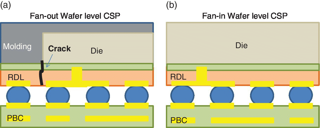
Figure 4.44 Failure mechanism for fan‐out but not for fan‐in wafer level packaging: (a) example of cracking on fan‐out wafer and (b) illustration of no cracking on fan‐in wafer.
Based on T. Strothmann and H. Clauberg (Kulicke&Soffa), CSTIC, March 2016 [77].
The chip‐to‐board interaction was studied and improved by various passivation techniques, tuning the process window, optimizing the redistribution layer patterns, and by using suitable solder ball material. A simulation model was developed with design guidelines for reducing the problem.
In 2017, Nanyang TU and ChipPAC discussed the effect of a high temperature storage (HTS) test on FO‐WLP package strength [79]. There were three different structures of FO‐WLP studied, as shown in Figure 4.45.

Figure 4.45 An overmolded FO‐WLP with 490 µm thickness and two thin FO‐WLP both ground to 200 µm thickness. On wafer 3 a thin backside protection tape was laminated.
Based on C. Xu et al. (Nanyang Technology University), CSTIC, March 2017 [79].
High temperature storage (HTS) for 1000 hours was done according to the JEDEC standard for high temperature storage life (JESD22‐A103). A three‐point bending test was used to evaluate the flexing strength. It was conducted at room temperature at three readout points in the high temperature storage test – at 0, 500, and 1000 hours. Results indicated that FO‐WLP flex strength increased with an increase in high temperature storage test time. The thick FO‐WLP showed the highest flex strength. The back‐side protection tape did not increase the flexure strength but was shown to have a tighter flexure strength distribution.
In 2017, NCTU and Kingyoup Optronics discussed release layers in a temporary bonding scheme involving mechanically supported thin wafer handling for applications such as FO‐WLP, 2.5D interposers with TSV, and 3D‐IC high density integration with TSV interconnects [80]. The release layer studied was an inorganic amorphous silicon together with a type of polyimide adhesive based on high 355 nm wavelength laser absorption.
An illustration of the process flow for temporary bonding is shown in Figure 4.46 where (a) shows the device wafer and the glass handler, (b) shows the use of the spin‐coated adhesive layer applied to the device wafer and the release layer deposited by HDP‐CVD to the glass wafer, (c) shows the layers temporarily bonded, and (d) shows the separation using a room temperature laser release process.
Figure 4.46 Illustration of process flow for temporary bonding before and after the laser ablation process.
Based on C.‐A. Cheng et al. (NCTU, Kingyoup Optronics), Journal of Electron Devices Society, 5 (2), March 2017 [80].
Bonding was done under a temperature of 210 °C using a 1 MPa bonding force. Also checked for the bonded structure were: chemical resistance for BEOL processes, mechanical bonding strength between the carrier wafer and an ultrathin device with thickness below 100 µm, and thermal stability up to 300 °C. Release process temperature and high throughput are also significant factors.
In May of 2016, the Fraunhofer Institute and TU Berlin discussed a foldable FO‐WLP [81]. In FO‐WLP, known good bare dies are embedded into a mold compound to form a reconfigured wafer. A redistribution layer is applied on the reconfigured die, which routes the die pads to the space both around and on the die. Bumps are then formed and the system is singulated. This technology can be used for multichip packages, referred to as system‐in‐package (SiP) or package‐on‐package (PoP), which is usually accomplished by stacking and using TSV. This study looks at a foldable FO‐WLP that uses a single sided planar process to achieve a stacked 3D package by folding alone. The folding can be done by using a flexible redistribution layer and a singulation process that cuts through only the molding compound leaving the redistribution layer untouched. The feasibility was checked using a multichip package with the dies connected by wiring done by laminating a polyimide film over the embedded chips. Microvias were then drilled to the die pads using a UV laser and metallized by Cu electroplating. The Cu was etched to form wire and pads. The wafer was diced in two steps: bending cuts were done by dicing through only the molding compound and then the package was folded. This technique can also be used to integrate multiple die packages on to free form surfaces.
To be able to make high performance circuits using ultrathin silicon chips in flexible electronic circuits, simulation and modeling of changes on device and circuit characteristics in response to bending induced stress is needed. In 2017, the University of Glasgow discussed issues in developing a compact model of CMOS devices and circuits on flexible thin chips [82]. Compressive and tensile stress studies on transistors and simple circuits were done. Different designs of devices and circuits in standard 180 nm CMOS were made in two separated chips. The chips were thinned to 20 µm using a conventional dicing‐before‐grinding technique followed by post‐CMOS thinning required to obtain a bendability of 20 mm bending radius. The thinned chips were packaged on a flexible substrate. Results showed a change of carrier mobilities in various transistors and change of switching threshold voltage of inverters during different bending conditions. A compact model was developed that predicts the variation in mobility and threshold voltage using compressive and tensile behind stress conditions and orientations. The model showed agreement with the experimental measurements.
References
- 1 Hou, Y., Lu, Z., Pu, T. et al. (2013) Fast switching protocol for ferroelectric random access memory based on poly(vinylidene fluoride‐trifluoroethylene) copolymer ultrathin films (East China University of S&T). Applied Physics Letters, 102 (6), 063507, February 2013.
- 2 Chen, X. et al. (2013) P(VDF‐TrFE‐CFE) terpolymer thin‐film for high performance non‐volatile memory (Nanjing University). Applied Physics Letters, 102, (6), 063101, February 2013.
- 3 von Nordheim, D. et al. (2013) Retention of thin ferroelectric VDF‐TrFE copolymer films evaluated from dielectric non‐linearities (University of Applied Science, Jena), ISAF/PFM, pp. 208, July 21, 2013.
- 4 Bak, J.Y. and Yoon, S.M. (2013) Nonvolatile memory characteristics of thin‐film transistors using hybrid gate stack composed of solution‐processed indium–zinc–silicon oxide active channel and organic ferroelectric gate insulator (Kyung Hee University). Journal of Vacuum S&T, 31 (4), 040601, July 2013.
- 5 Jandhyala, S. et al. (2013) Graphene‐ferroelectric hybrid devices for multi‐valued memory system (University of Texas Dallas). Applied Physics Letters, 103 (2), 022903, July 2013.
- 6 Hou, Y. et al. (2013) Unipolar poling‐induced high switching speed and improved imprint behaviors for poly(vinylidene fluoride‐trifluoroethylene) copolymer ultrathin films (East China University). Applied Physics Letters, 103 (26), 263503, December 2013.
- 7 Nedic, S. et al. (2014) High performance non‐volatile ferroelectric copolymer memory based on a ZnO nanowire transistor fabricated on a transparent substrate (University of Cambridge). Applied Physics Letters, 104 (3), 033101, January 2014.
- 8 Zhang, X. et al. (2014) Temperature dependence of imprint mechanism in poly(vinylidene fluoride‐trifluoroethylene) copolymer ultrathin films (Shanghai University of Engineering Science). Applied Physics Letters, 104 (10), 103505, March 2014.
- 9 Petti, L. et al. (2014) Influence of mechanical bending on flexible InGaZnO‐based ferroelectric memory TFTs (Institute of Technology, Zurich). IEEE Trans. on Electron Devices, 61 (4), 1085, April 2014.
- 10 Cai, R. et al. (2014) An organic ferroelectric field effect transistor with poly(vinylidene fluoride‐co‐trifluoroethylene) nanostripes as gate dielectric (Université Catholique de Louvain). Applied Physics Letters, 105 (11), 113113, September 2014.
- 11 Mao, D. et al. (2014) Low temperature processed two‐transistor‐two‐capacitor‐based ferroelectric random access memory (Micron., University of Texas Dallas). IEEE Trans. on Electron Devices, 61 (10), 3442, October 2014.
- 12 Micjan, M. et al. (2014) Ferroelectric polymer films for flexible memory devices (Slovak University of Technology), ASDAM, October 20, 2014.
- 13 Bringans, R.D. and Verese, J. (2016) Challenges and opportunities in flexible electronics, IEEE IEDM (PARC), December 2016.
- 14 Printed sensor system rolls off the press, Thinfilm Electronics Press Release, December 20, 2012.
- 15 Thinfilm demonstrates first integrated printed electronic system with rewritable memory, Thin Film Press Release, December 20, 2012.
- 16 Takahashi, D. (2012) Thin Film Electronics demonstrates a way to make disposable interactive smart labels that replace bar codes, Thin Film Electronics, December 19, 2012.
- 17 Guerin, M. et al. (2013) Organic complementary logic circuits and volatile memories integrated on plastic foils (Aix‐Marseille Université, IM2NP, CNRS, IM2NP, LTEN‐LCEI, CEA‐Grenoble). IEEE Trans. on Electron Devices, 60 (6), June 2013.
- 18 Myny, K. et al. (2014) Thin‐film microprocessor using a hybrid oxide‐organic complementary technology with inkjet‐printed P2ROM memory (IMEC, Panasonic, KU Leuven, Evonik, Holst), ISSCC, February 2014.
- 19 Takahashi, D. (2015) Thinfilm teams with Xerox so it can print a billion chips a year for the Internet of Things, https//VentureBeat.com, January 21, 2015.
- 20 Savastano, Xerox, Thinfilm look to bring Xerox printed memory to market, http//www.printedelectronicsnow.com, September 23, 2015.
- 21 Xerox launches printed memory products to combat counterfeiting, Xerox Press Release, September 15, 2015.
- 22 Xerox to set up 1.3 billion capacity Thinfilm smart label print line, Plastic Electronics, https//www.plusplasticelectronics.com, January 21, 2016.
- 23 Hilson, G. (2016) Printed memory to secure IoT, EE Times, June 13, 2016
- 24 Takahashi, D. (2017) Thinfilm's tiny printed NFC labels enable brands to connect with consumers via smart packaging, March 23, 2017.
- 25 Huang, T.C. et al. (2016) Printed circuits on flexible substrates: opportunities and challenges (Hewlett Packard, Hong Kong University of S&T), Symposium on Networks‐on‐Chips (NOCS), October 2016.
- 26 Lee, S.H. et al. (2015) Pixel architecture for low‐power liquid crystal display comprising oxide and ferroelectric memory thin film transistors (Kyung Hee University, Electronics and Telecommunications Research Institute, Daijeon). IEEE Electron Device Letters, 36 (6), 585, June 2015.
- 27 Izumi, S., Kimura, H. et al. (2015) A ferroelectric‐based non‐volatile flip‐flop for wearable healthcare systems (Kobe University, ROHM), Non‐volatile Memory Technology Symposium, October 2015.
- 28 Kyeong‐Ah Kim et al. (2016) Read‐out modulation scheme for the display driving circuits composed of nonvolatile ferroelectric memory and oxide‐semiconductor thin‐film transistors for low‐power consumption (Kyung Hee University, Electronics and Telecommunication Research Institute), IEEE Trans. on Electron Devices, 61 (1), January 2016.
- 29 Li, C. et al. (2015) Ultrathin BaTiO2‐based ferroelectric tunnel junctions through interface engineering (NUS, Trinity College Dublin). ACS Nanoletters, Nano Lett., 15 (4), 2568–2573, March 2015.
- 30 Tian, T.T. et al. (2016) Tunnel electroresistance through organic ferroelectrics (CAS, Université Paris‐Saclay, East China Normal University). Nature Communications, 7, 11502, May 4, 2016.
- 31 Huang, R., Tang, Y., Kuang, Y. et al. (2012) Resistive switching in organic memory device based on parylene‐C with highly compatible process for high‐density and low‐cost memory applications (Peking University, Princeton University). IEEE Trans. on Electron Devices, 59 (12), 3578, December 2012.
- 32 Bai, W., Huang, R., Cai, Y. et al. (2013) Record low‐power organic RRAM with sub‐20 nA reset current (Peking University), IEEE Electron Device Letters, 34 (2), 223, February 2013.
- 33 Huang, R. et al. (2014) Resistive switching in organic memory devices for flexible applications (Peking University), ISCAS, June 2014.
- 34 Sakamoto, T., Tada, M., Okamoto, K. and Hada, H. (2012) Electronic conduction mechanism in atom switch using polymer solid electrolyte (LEAP). IEEE Trans. on Electron Devices, 59 (12), 3574, December 2012.
- 35 Banno, N. et al. (2015) Cu atom switch with steep time‐to‐ON‐state versus switching voltage using Cu ionization control (LEAP). IEEE Trans. on Electron Devices, 62 (9), September 2015.
- 36 Tada, M. et al. (2015) ON‐state reliability of Cu atom switch under current–temperature stress (NEC). IEEE Trans. on Electron Devices, 62 (9), September 2015.
- 37 Okamoto, K. et al. (2016) Robust Cu atom switch with over‐400 °C thermally tolerant polymer‐solid electrolyte (TT‐PSE) for nonvolatile programmable logic (NEC), VLSI‐T, June 2016.
- 38 Tada, M. and Sakamoto, T. (2017) Set/reset switching model of Cu atom switch based on electrolysis (NEC). IEEE Trans. on Electron Devices, 64 (4), April 2017.
- 39 Chou, K.I., Cheng, C.H., Zheng, Z.W. et al. (2013) Ni/GeOx/TiOy/TaN RRAM on flexible substrate with excellent resistance distribution (NCTU, National Taiwan Normal University, IM‐CAS). IEEE Electron Device Letters, 34 (4), 505, April 2013.
- 40 Liu, Y. et al. (2014) Inorganic–organic hybrid switching memory with high uniformity and multilevel operation (IM Peking University), VLSI‐TSA, April 28, 2014.
- 41 Lin, C.C. (2014) Resistive switching behavior of Al/Al2O3/ZrO2/Al structural device for flexible nonvolatile memory application (National Dong Hwa University). IEEE Trans. on Magnetics, 50 (7), July 2014.
- 42 Hou, T.H. et al. (2013) Low‐cost embedded RRAM technology for system‐on‐plastic integration using a‐IGZO TFTs (NCTU), AM‐FPD, July 2, 2013.
- 43 Wu, S.C. et al. (2013) Flexible three‐bit‐per‐cell resistive switching memory using a‐IGZO TFTs (NCTU). IEEE Electron Device Letters, 34 (10), 1263, October 2013.
- 44 Kim, S.J., Won‐Ho Lee and Sung‐Min Yoon (2015) Nonvolatile memory performances of transparent and/or flexible memory thin‐film transistors using IGZO channel and ZnO charge‐trap layers (Kyung Hee University), AMFPD, July 2015.
- 45 Rocha, P.R.F. et al. (2013) The role of internal structure in the anomalous switching dynamics of metal‐oxide/polymer resistive random access memories (Institute de Telecom, Lisboa, Portugal). Journal of Applied Physics, 113 (13), 134504, April 2013.
- 46 Bogusz, A. et al. (2013) Resistive switching in thin multiferroic films (Chemnitz University of Technology, University of Electronic S&T Chengdi, Institute of Ion‐Beam Physics and Materials Research Dresden, Institute of Integrated Nanosciences Dresden), ISCDG, September 26, 2013.
- 47 Mutiso, R.M. et al. (2013) Resistive switching in silver/polystyrene/silver nano‐gap devices (University of Pennsylvania). Applied Physics Letters, 103 (22), 223302, November 2013.
- 48 Song, H.J. (2013) Switchable diode effect in polycrystalline Bi3.15Nd0.85Ti3O12 thin films for resistive memories (Xiangtan University). Applied Physics Letters, 103 (26), 262901, December 2013.
- 49 Tsai, H.Y. et al. (2014) Resistive switching behaviors of Au/pentacene/Si‐nanowire arrays/heavily doped n‐type Si devices for memory applications (National Changhua University of Education). Applied Physics Letters, 104 (5), 053501, February 2014.
- 50 Huang, J. and Ma, D. (2014) Electrical switching and memory behaviors in organic diodes based on polymer blend films treated by ultraviolet ozone (Changchun Institute of Applied Chemistry). Applied Physics Letters, 105 (9), 093303, September 2014.
- 51 Santoni, F. et al. (2016) Modeling of filamentary conduction in organic thin film memories and comparison with experimental data (University of Rome, TU Munchen, CNR‐ISMN, NanoTecCenter Weiz, Graz University of Technology). IEEE Trans. on Nanotechnology, 15 (1), January 2016.
- 52 Chao, H., Chongjie Wang, Wei, R. et al. (2016) Bipolar resistive switching in Al/GO‐PEDOT: PSS/Pt memory devices (Tsinghua University, Beijing University of Chemical Technology, Fuzhou University), EDSSC, August 2016.
- 53 Lee, W.H., Kim, E.J. and Yoon, S.M. (2016) Multilevel resistive‐change memory operation of Al‐doped ZnO thin‐film transistor (Kyong Hee University). IEEE Electron Device Letters, 37 (8), August 2016.
- 54 Shih, C.C. et al. (2016) Ultra‐low switching voltage induced by inserting SiO2 layer in indium‐tin‐oxide‐based resistance random access memory (Nat.ional Sun Yat‐Sen University, University of Texas, Austin, National Cheng Kung University, National Kaohsiung Normal University, Xiamen University). IEEE Electron Device Letters, 37 (10), October 2016.
- 55 Vescio, G. et al. (2017) Inkjet printed HfO2‐based ReRAMs: First demonstration and performance characterization (University de Barcelona, University Autonoma de Barcelona). IEEE Electron Device Letters, 38 (4), April 2017.
- 56 Lee, K.J. et al. (2017) Effects of Ni in strontium titanate nickelate thin films for flexible nonvolatile memory applications (National Cheng‐Kung University, National University of Kaohsiung, Air Force Institute of Technology, Kaohsiumg). IEEE Trans. on Electron Devices, 64 (5), 2001, May 2017.
- 57 Semple, J. et al. (2017) Semiconductor‐free nonvolatile resistive switching memory devices based on metal nanogaps fabricated on flexible substrates via adhesion lithography (Imperial College London, King Abdullah University of S&T). IEEE Trans. on Electron Devices, 64 (5), 1973, May 2017.
- 58 Brunel, B., Levesque, P.L., Ardiaca, F. et al. (2013) Control over the interface properties of carbon nanotube‐based optoelectronic memory devices (CEA, IRAMIS, CNRS, LEM). Applied Physics Letters, 102 (1), 013103, January 2013.
- 59 Cosmin Obreja, A. et al. (2014) Charge transport and memristive properties of graphene quantum dots embedded in poly(3‐hexylthiophene) matrix (National Institute for R&D in Microtech, Romania). Applied Physics Letters, 105 (8), 083303, August 28, 2014.
- 60 Lin, J. et al. (2015) Solution‐processed, flexible, and transparent non‐volatile memory with embedded graphene quantum dots in polymethylsilsesquioxane layers (Fuzhou University, Hanyang University). IEEE Electron Device Letters, 36 (11), November 2015.
- 61 Wang, Y. et al. (2013) Ink‐jet printed In‐Ga‐Zn oxide nonvolatile TFT memory utilizing silicon nanocrystals embedded in SiO2 gate dielectric (Technology University of Singapore), Nanoelectronics Conference (INEC), pp. 222, January 2, 2013.
- 62 Yun, D.Y. (2014) Multilevel charging and discharging mechanisms of nonvolatile memory devices based on nanocomposites consisting of monolayered Au nanoparticles embedded in a polystyrene layer (Hanyang University). Applied Physics Letters, 104 (2), 023304, January 20, 2014.
- 63 P. Bousoulas, P. et al. (2015) Improving the resistive switching uniformity of forming‐free TiO2‐x based devices by embedded Pt nanocrystals (National Technical University of Athens), ESSDIRC, September 2015.
- 64 Shih, C.C. et al. (2016) High performance transparent transistor memory devices using nano‐floating gate of polymer/ZnO nanocomposites (National Sun Yat Sen University), Scientific Reports, February 1, 2016.
- 65 Kim, S.J. et al. (2016) High performance and stable flexible memory thin‐film transistors using In‐Ga‐Zn‐O channel and ZnO charge‐trap layers on poly (ethylene naphthalate) substrate (Kyung Hee University, Electronics and Telecomm Research Institute). IEEE Trans. on Electron Devices, 63 (4), April 2016.
- 66 Wang, D.T. et al. (2016) Resistive switching and synaptic behaviors of TaN/Al2O3/ZnO/ITO flexible devices with embedded Ag nanoparticles (Fudan University), IEEE Electron Device Letters, 37 (7), 878, July 2016.
- 67 Woo, M.H. et al. (2016) Floating gate memory based on MoS2 channel and iCVD polymer tunneling dielectric (KAIST), ESSDERC, September 2016.
- 68 Choi, J.M., Han, J.W. and Choi, Y.K. (2014) Flexible high‐performance nonvolatile memory by transferring GAA silicon nanowire SONOS onto a plastic substrate (KAIST), IEDM, December 2014.
- 69 Kim, D.H. et al. (2015) ACF‐packaged ultrathin Si‐based flexible NAND Flash memory (KAIST), IEEE IEDM, December 2015.
- 70 Burghartz, J.N. (2013) Make way for flexible silicon chips (Institut fur Mikroelektronik Stuttgart), IEEE Spectrum, February 25, 2013.
- 71 Gupta, U. et al. (2016) Can systems extend to polymer? SoP architecture design and challenges (Arizona State University), IEEE SOCC, February 2016.
- 72 Putalla, J. et al. (2017) Capability assessment of inkjet printing for reliable RFID applications (University of Oulu, Meyer Burger BV, Tampere University). IEEE Trans. on Device and Materials Reliability, 17 (2), 281, June 2017.
- 73 Vilouras, A. et al. (2017) Modeling of CMOS devices and circuits on flexible ultrathin chips (University of Glasgow). IEEE Trans. on Electron Devices, 64 (5), May 2017, 2038, February 23, 2017.
- 74 Watanabe, I. et al. (2017) Latest material technologies for fan‐out wafer level package (Sumitomo Bakelite Co.), Semiconductor Technology International Conference (CSTIC), March 12, 2017.
- 75 Fan‐out wafer level packaging: Breakthrough advantages and surmountable challenges (SPTS Technology), Press Release, August 2016.
- 76 Lee, M. et al. (2015) Novel adaptive probing for wafer level chip scale package (TSMC), eMDC&ISSM, September 2015.
- 77 Strothmann, T. and Clauberg, H. (2016) High throughput thermocompression bonding enabled with a flexible manufacturing platform (Kulicke&Soffa), CSTIC, March 2016.
- 78 Yu, C.K. et al. (2017) A unique failure mechanism induced by chip to board interaction on fan‐out wafer level package (MediaTek), IRPS, April 2017.
- 79 Xu, C., Zhong, Z.W. and Choi, W.K. (2017) Effect of high temperature storage on fan‐out wafer level package strength (Nanyang Technology University), CSTIC, March 2017.
- 80 Cheng, C.‐A. et al. (2017) Feasibility investigation of amorphous silicon as release layer in temporary bonding for 3‐D integration and FOWLP scheme (National Chiao Tung University, Kingyoup Optronics). Journal of Electron Devices Society, 5 (2), March 2017.
- 81 Braun, T. et al. (2016) Foldable fan‐out wafer level packaging (Fraunhofer Institüt Berlin, TU Berlin), ECTC, May 2016.
- 82 Vilouras, A. et al. (2017) Modeling of CMOS devices and circuits on flexible ultrathin chips (University of Glasgow). IEEE Trans. Electron Devices, 64, (5), May 2017.