
In Chapter 24, we discussed two kinds of transistors—bipolar junction transistors (BJTs) and field effect transistors (FETs). The previous chapters have focused primarily on BJTs because they are, in fact, great at various tasks that are commonly considered “amplification.”
However, there are two amplification tasks for which BJTs are terribly suited—switching and logic circuits. Many people don’t think of amplification when they think of logic circuits, but, indeed, they do require amplification. Think about the memory of a computer (which is a type of logic circuit). The memory of the computer has to continue to last after it has been written to. If there was no amplification, the signal would fade over time.1 Therefore, in order to just “hold on” to the signal, amplification is required.
While this can be done with BJTs, since BJTs are current amplifiers, they tend to utilize a lot of current to get this done. Field effect transistors (FETs) operate instead on voltage and require very little current to operate. Therefore, they are very efficient for logic-type applications.
27.1 Operation of a FET
A FET has a very similar set of parts to a BJT. There are three parts—a gate, a source, and a drain.2
The basic operation of the FET is that a voltage at the gate controls the current conduction between the drain and the source. The gate controls the conduction between the drain and the source. Like BJTs, FETs have fully off, fully on, and partially on states. However, unlike BJTs, even when “fully on,” FETs still offer a resistance between the drain and the source. This is why, for current-focused applications, BJTs are often used—in their fully on state, they don’t limit the current from the collector to the emitter.
Unlike the BJT, the FET is operated by voltages rather than current. Because of this, the gate essentially consumes almost no current whatsoever (it can have a Thévenin equivalence of hundreds of megaohms of resistance). So, while BJTs consume current to perform their operation, FETs consume almost none.
A depletion mode FET is normally “on” (allowing current to flow between the drain and the source), but turns off when a sufficient voltage (compared to the source) is applied at the gate. The voltage works to “deplete” the transistor of its conducting ability.
An enhancement mode FET is normally “off” (blocking current flow between the drain and the source), but turns on when a sufficient voltage (compared to the source) is applied at the gate. The voltage works to “enhance” the transistor’s ability to conduct.
FETs are distinguished as N-channel or P-channel based on their orientation. In an N-channel FET, the current flows from the drain to the source (i.e., the drain acts like the collector, and the source acts like the emitter). In a P-channel FET, the current flows from the source to the drain (i.e., the source acts like the collector, and the drain acts like the emitter). For an enhancement mode FET, the gate activates the channel when the gate voltage (compared to the source) is sufficiently positive if it is an N-channel and sufficiently negative if it is a P-channel. For a depletion mode FET, the gate closes the channel when the gate voltage (compared to the source) is sufficiently negative if it is an N-channel and sufficiently positive if it is a P-channel.3
So, for instance, in a P-channel depletion mode FET, the source will be positive, the drain will be negative, and the channel will close as the gate voltage becomes more and more negative compared to the source.
Additionally, most FETs have a “threshold voltage” that the gate must achieve before it switches on.
In addition to the channel and the mode, FETs are made in a variety of different ways, which leads to numerous different types of FETs—MOSFETs, JFETs, QFETs, MNOSs, and others. Each of these has its own distinct operating characteristics (threshold voltage, channel resistance, etc.). We will focus on one particular FET to make life easier—the N-channel enhancement mode MOSFET. This is the most commonly used FET by hobbyists.
27.2 The N-Channel Enhancement Mode MOSFET

The Schematic Symbol for an N-Channel MOSFET Transistor
Figure 27-1 shows the schematic symbol for the N-channel MOSFET. Notice that the arrow is pointing out from the source. Again, that is because in this transistor, the source performs the same function as the emitter on a BJT.
27.3 Using a MOSFET
Figure 27-2 shows a schematic of a simplistic usage of a MOSFET. In this figure, the gate of the MOSFET is controlled by a switch. When the switch is on, the MOSFET conducts. However, the important thing to note is that the pathway into the gate of the MOSFET consumes basically no current whatsoever!
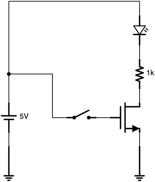
A Simple MOSFET Circuit

A Microcontroller Pin Controlling a MOSFET
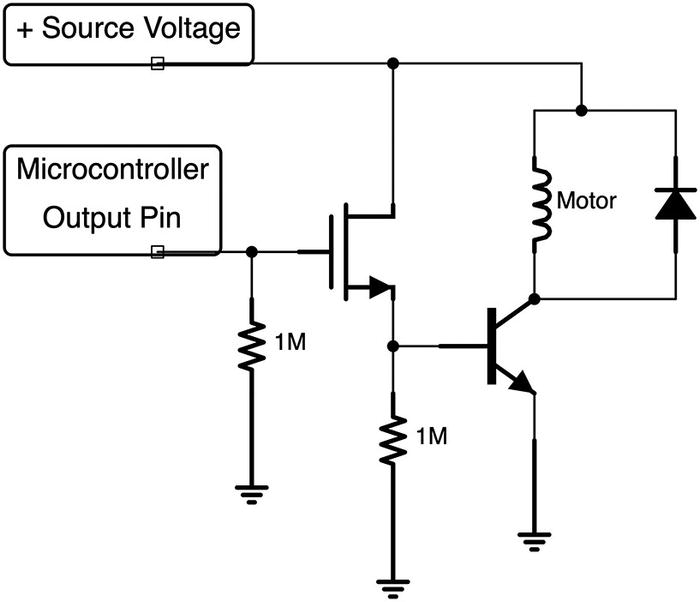
Combining a MOSFET with a BJT to Power a Motor
One issue, however, is that, as we mentioned, MOSFETs always have resistance between the drain and source, limiting the amount of current that a MOSFET can source. If we wanted to power a motor, for instance, we would need to increase the current. We can do this by adding a BJT to the output of our MOSFET. Figure 27-4 shows this configuration. Notice that both transistors have a pull-down resistor attached. This prevents any accidental conduction of our devices.

A MOSFET with Two BJTs for Higher Current
However, even this configuration may not provide enough current. The transistor can only amplify what it gets from the MOSFET, and the current output from the MOSFET is sometimes just not high enough for a single-stage amplification. Therefore, we can use the output from the first BJT as an input to the base of a second BJT to open up the power even more. Figure 27-5 shows this configuration. Note that each transistor has a pull-down resistor to make sure that it gets shut off when the pin goes low.
This configuration provides practically unlimited current through the collector of the transistor and doesn’t utilize any current output from the microcontroller.
27.4 MOSFETs in Logic Circuits
MOSFETs are also great to use in logic circuits, again, because they use practically no current at all. While the pathway from the drain to the source can draw current, if the output coming from the source goes to another MOSFET, then it won’t utilize any current either. As we mentioned earlier, we can think of the gate of a MOSFET as having a resistance on the order of a hundred megaohms. Therefore, Ohm’s law will prevent any significant amount of current running into them.
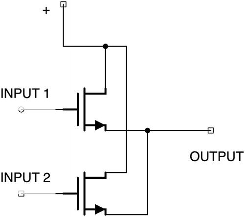
In Chapter 12, we learned about integrated circuits that could perform logic functions such as AND, OR, and NOT. We can mimic these same logic functions with MOSFET transistors (we can also mimic them with BJTs, but we would waste a lot of current doing it).

An AND Gate Using MOSFETs
An OR Gate Using MOSFETs

A NOT Gate Using MOSFETs
Review
- 1.
Field effect transistors (FETs) are similar to BJTs, but they are controlled by voltage instead of current.
- 2.
The parts of the FET transistor are the gate, the source, and the drain, though whether the source or the drain is on the positive side depends on the type of transistor.
- 3.
The N-channel depletion mode MOSFET is wired (somewhat confusingly) so that the drain is on the positive side and the source is on the negative side. Applying a positive voltage at the gate allows current to flow from the drain to the source.
- 4.
Because FETs operate using voltage, the gate consumes almost no current, making it ideal for controlling devices from microcontrollers.
- 5.
When a device is truly power-hungry, a FET can be used in combination with one or two BJTs to provide additional current output to the device.
- 6.
FETs can also be used in combination with each other to produce logic circuits that utilize very little current.
Apply What You Have Learned
- 1.
Why is it especially important to include pull-down resistors with FET transistors?
- 2.
Which types of FETs are normally conducting between the drain and the source? Which ones are normally not conducting?
- 3.
Create a circuit that combines an AND gate and an OR gate using N-channel MOSFETs. It should turn on an LED if buttons 1 and 2 are pressed or if button 3 is pressed.
- 4.
Why is a BJT needed to power an electric motor in addition to the MOSFET?