
Chapter 5: Implementing systems with FPGAs
This chapter dives into the process of designing and implementing systems with FPGAs. It begins with a description of the FPGA compilation software tools that convert a description of a logic design in a programming language into an executable FPGA configuration. We will discuss the types of algorithms best suited to FPGA implementation and suggest a decision approach for determining whether a particular embedded system algorithm is more appropriately implemented using a traditional processor or with an FPGA. The chapter ends with the step-by-step development of a baseline FPGA-based processor project that will be expanded to implement a high-speed digital oscilloscope using circuitry and software developed in later chapters.
After completing this chapter, you will have learned about the processing steps performed by FPGA compilation tools and will understand the types of algorithms best suited to FPGA implementation. You will know how to determine whether FPGA implementation is right for a given design and will have worked through a real FPGA system development project for a high-performance processing application.
We will cover the following topics in this chapter:
- The FPGA compilation process
- Algorithm types most suitable for FPGA implementation
- Kicking off the oscilloscope FPGA project
Technical requirements
We will be using Xilinx Vivado and an Arty A7-100 development board in this chapter. See Chapter 4, Developing Your First FPGA Program, for information on Vivado download and installation.
The files for this chapter are available at https://github.com/PacktPublishing/Architecting-High-Performance-Embedded-Systems.
The FPGA compilation process
The process of compiling a digital circuit model begins with a specification of circuit behavior in a hardware description language, such as VHDL or Verilog, and produces as its output an implementation of that circuit that can be downloaded and executed in an FPGA. The software tool set that performs the synthesis process is sometimes called a silicon compiler or hardware compiler.
FPGA compilation takes place in three steps: synthesis, placement, and routing. Chapter 4, Developing Your First FPGA Program, introduced these steps. Behind the scenes, the software tools that perform the steps implement a collection of sophisticated algorithms to produce an optimized FPGA configuration that correctly implements the circuit described by the source code.
Before you can begin the compilation process, the first step is to create a complete description of the circuit, typically as a collection of files in the VHDL or Verilog languages. This is called design entry.
Design entry
We will continue with the 4-bit adder circuit we used for the example project in Chapter 4, Developing Your First FPGA Program. The purpose of this example is to clarify that, as in traditional software development, there are multiple ways to solve a given problem in hardware description languages. As we'll see, it is generally better to choose an implementation that is clear and understandable for the developer than to try to create a more optimized but also more complicated design. We'll also introduce some new constructs in the VHDL language.
From a review of the code in Adder4.vhdl, listed in the Creating VHDL source files section of Chapter 4, Developing Your First FPGA Program, you will observe that the carry output from each full adder (the signal named C_OUT) is used as an input for the next full adder (as the signal named C_IN). As a result of this configuration, which is referred to as a ripple-carry adder, it is possible for a carry from the least significant adder to propagate through all of the higher-order adders. For example, this occurs when 1 is added to the binary value 1111. The circuitry interacting with the adder must therefore wait for this maximum propagation delay after presenting inputs to the adder before it can reliably read the adder output.
If we look at this problem at a higher level of abstraction, we can examine alternative implementations that produce the same computed result in a different manner. Instead of specifying the exact set of logic operations to perform the addition operation, in terms of AND, OR, and XOR operators, as we did in FullAdder.vhdl, we can instead create a Lookup Table (LUT) that uses an input of 8 bits, formed by concatenating the two 4-bit addends, with output consisting of the 4-bit sum and the 1-bit carry. The following listing shows how this table is represented in VHDL:
-- Load the standard libraries
library IEEE;
use IEEE.STD_LOGIC_1164.ALL;
-- Define the 4-bit adder inputs and outputs
entity ADDER4LUT is
port (
A4 : in std_logic_vector(3 downto 0);
B4 : in std_logic_vector(3 downto 0);
SUM4 : out std_logic_vector(3 downto 0);
C_OUT4 : out std_logic
);
end entity ADDER4LUT;
-- Define the behavior of the 4-bit adder
architecture BEHAVIORAL of ADDER4LUT is
begin
ADDER_LUT : process (A4, B4) is
variable concat_input : std_logic_vector(7 downto 0);
begin
concat_input := A4 & B4;
case concat_input is
when "00000000" =>
SUM4 <= "0000"; C_OUT4 <= '0';
when "00000001" =>
SUM4 <= "0001"; C_OUT4 <= '0';
when "00000010" =>
SUM4 <= "0010"; C_OUT4 <= '0';
.
.
.
when "11111110" =>
SUM4 <= "1101"; C_OUT4 <= '1';
when "11111111" =>
SUM4 <= "1110"; C_OUT4 <= '1';
when others =>
SUM4 <= "UUUU"; C_OUT4 <= 'U';
end case;
end process ADDER_LUT;
end architecture BEHAVIORAL;
In this listing, 250 of the 256 table entries were elided as indicated by the vertical …
The case statement in this code is enclosed in a process statement. process statements provide a way to insert collections of sequentially executed statements within the normal VHDL construct of concurrently executing statements. The process statement includes a sensitivity list (containing A4 and B4 in this example) that identifies the signals that trigger the execution of the process statement whenever they change state.
Although a process statement contains a set of statements that execute sequentially, the process statement itself is a concurrent statement that executes in parallel with the other concurrent statements in the design once its execution has been triggered by a change to a signal in its sensitivity list. If the same signal is assigned different values multiple times within a process body, only the final assignment will take effect.
You may wonder why it is necessary to include the when others condition at the conclusion of the case statement. Although all 256 possible combinations of 0 and 1 bit values are covered in the when conditions, the VHDL std_logic data type includes representations of other signal conditions, including uninitialized inputs. The when others condition causes the outputs of the adder to return unknown values if any input has a value other than 0 or 1. This is a form of defensive coding that will cause a simulation run to alert us if we forget to connect any of the inputs to this logic component, or use an uninitialized or otherwise inappropriate value as an input.
These rules and behaviors are likely to be unfamiliar to anyone comfortable with traditional programming languages. When implementing and testing VHDL designs, you can expect to experience some confusing experiences where things don't seem to be functioning as you expect. You'll need to keep in mind that with VHDL you are defining digital logic that acts in parallel, not a sequentially executing algorithm. It is also important to thoroughly simulate circuit behavior and ensure your code is operating properly before attempting to run it in an FPGA.
Getting back to our example, while it might be reasonable to include a 256-element lookup table in the design of a 4-bit adder, the size of the lookup table quickly becomes unmanageable if the data words to be added consist of 16, 32, or 64 bits. Rather than using large lookup tables, practical digital adder circuits use more sophisticated logic than the ripple-carry adder, in the form of a carry look-ahead adder, to improve execution speed. The carry look-ahead adder includes logic to anticipate the propagation of carries, thereby reducing the time taken to produce a final result.
We will not be getting into the details of carry look-ahead adder construction, but we will note that the VHDL language contains an addition operator, and you can expect the implementation resulting from the use of this operator to be highly optimized for the targeted FPGA model. The following code is a 4-bit adder using the native VHDL addition operator rather than a collection of gate-level single-bit adders or a lookup table to perform the addition operation:
-- Load the standard libraries
library IEEE;
use IEEE.NUMERIC_STD.ALL;
-- Define the 4-bit adder inputs and outputs
entity ADDER4NATIVE is
port (
A4 : in std_logic_vector(3 downto 0);
B4 : in std_logic_vector(3 downto 0);
SUM4 : out std_logic_vector(3 downto 0);
C_OUT4 : out std_logic
);
end entity ADDER4NATIVE;
-- Define the behavior of the 4-bit adder
architecture BEHAVIORAL of ADDER4NATIVE is
begin
ADDER_NATIVE : process (A4, B4) is
variable sum5 : unsigned(4 downto 0);
begin
sum5 := unsigned('0' & A4) + unsigned('0' & B4);
SUM4 <= std_logic_vector(sum5(3 downto 0));
C_OUT4 <= std_logic(sum5(4));
end process ADDER_NATIVE;
end architecture BEHAVIORAL;
This example includes the IEEE.NUMERIC_STD package, which brings in the ability to use numeric data types such as signed and unsigned integers in addition to the logic data types defined in the IEEE.STD_LOGIC_1164 package. The example code performs type conversions from the std_logic_vector data type to the unsigned integer type and uses those numeric values to compute the sum5 intermediate value, which is the 5-bit sum of the A4 and B4 addends. Each addend is extended from 4 to 5 bits by prepending it with a single bit of zero using the syntax '0' & A4. The unsigned result is converted back to the 4-bit std_logic_vector result SUM4 and a single-bit std_logic carry output C_OUT4.
Summarizing this series of VHDL examples, we have seen three different implementations of the 4-bit adder circuit: first as a collection of four single-bit adder logic circuits, second as a lookup table that produces its output by simply looking up the results given the inputs, and, finally, using the native VHDL addition operator. While this has been a somewhat contrived example, it should be clear that any given algorithm can be described in a variety of ways in VHDL or other Hardware Description Languages (HDLs).
With the design entry completed, we are now ready to perform logic synthesis.
Logic synthesis
FPGA circuits of moderate to high complexity typically consist of both combinational logic, which was the subject of the example project in Chapter 4, Developing Your First FPGA Program, and sequential logic. The output of a combinational logic circuit depends only on its inputs at a given moment, as we saw with various combinations of switch and pushbutton inputs on the Arty A7 board as it performed the addition operation.
Sequential circuits, on the other hand, maintain state information representing the results of past operations that affects future operations. Sequential logic within a circuit, or within a functional subset of a circuit, almost always uses a shared clock signal to trigger the update of coordinated data storage elements. By using a clock signal, these updates occur simultaneously and at regular intervals defined by the clock frequency. Sequential logic circuits that update state information based on a common clock signal are referred to as synchronous sequential logic. Most sophisticated digital circuits can be represented as hierarchical arrangements of lower-level components consisting of combinational and synchronous sequential logic.
FPGA devices generally implement combinational logic using lookup tables, which represent the output of a logic gate configuration using a small RAM. For a typical 6-input lookup table, the RAM contains Instance 4 single-bit entries, where each entry contains the single-bit circuit output for one possible combination of input values. Figure 5.1 shows the inputs and output of this simple lookup table:
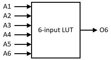
Figure 5.1 – 6-input lookup table
More complex combinational circuits can be constructed by combining multiple lookup tables in parallel and in series. The synthesis tool performs this step automatically for you.
FPGAs use flip-flops, block RAM, and distributed RAM to hold state information. Lookup tables and the components containing state information form the raw materials from which complex circuit designs are constructed by the silicon compiler.
Clock signals drive the operation of synchronous sequential logic within the digital circuit. In a typical FPGA design, a number of clock signals will be defined with frequencies that vary depending on the function that uses each signal. Clock signals internal to the FPGA may drive high-speed operations at frequencies in the hundreds of MHz. Other clock signals that drive interfaces to external peripherals, such as an Ethernet interface or DDR3 RAM, may have frequencies tailored to the needs of the external hardware. FPGAs generally contain clock generation hardware that supports the production of several clock frequencies for various uses.
Using vendor-provided FPGA development tools, system designers define the logic circuit, typically in VHDL or Verilog, and provide information describing the circuit clocking requirements and constraints associated with I/O interfaces and timing. The compilation tools provided by the vendor then perform the steps of synthesis, placement, and routing.
A significant portion of the processing effort involved in FPGA synthesis focuses on minimizing the amount of FPGA resources consumed by the implementation while meeting timing constraints. By minimizing resource consumption, the tools enable more complex designs to be implemented in smaller, less expensive devices. The next section will discuss some aspects of the design optimization process.
Design optimization
A significant portion of the processing that occurs during synthesis, implementation, and routing is devoted to optimizing the performance of the circuit. This optimization process has multiple goals, including minimizing resource usage, achieving maximum performance (in terms of maximum clock speed and minimum propagation delay), and minimizing power consumption.
By using an appropriate selection of constraints, discussed later in this chapter, it is possible for the designer to focus the optimization process on the goals most appropriate for the system under development. For example, a battery-powered system may put a premium on power consumption while being less concerned with achieving peak performance.
The optimization performed by these tools can be quite surprising to users unfamiliar with their capabilities. It is important to understand that the tools are not limited to implementing a circuit that resembles the way you have laid it out in VHDL code. The only requirement the tools must abide by is ensuring that the implemented circuit functions identically, in terms of input and output, to the design described in the code.
To emphasize this point, we can look at the performance (in terms of maximum propagation delay), resource utilization (in terms of the number of lookup tables used), and power consumption in milliwatts to compare the three forms of the 4-bit adder circuit design we developed in the earlier examples. We will continue with the 4-bit adder using the native VHDL addition operator listed earlier in this chapter.
Before we can do this, we first need to add two lines to the end of the Arty-A7-100.xdc constraints file:
create_clock -period 10 -name virtual_clock
set_max_delay 12.0 -from [all_inputs] -to [all_outputs]
The create_clock statement creates a virtual clock, which we have named virtual_clock, with a period of 10 ns. This is necessary because our circuit does not have any actual clock signals, but Vivado requires a reference clock to perform timing analysis, even if the clock is not really present. The set_max_delay statement defines a constraint stating that the maximum propagation delay we can tolerate for our FPGA implementation is 12 ns between any input and any output. We do not have a real need for propagation to take no more than 12 ns. We have chosen this limit because it is within the capabilities of the FPGA device.
Perform the following steps to implement the design:
- Save the preceding changes to the XDC file.
- Select Run Implementation. You will be prompted to rerun the synthesis step, which is necessary to incorporate the changed constraints.
- When implementation completes, select Open Implemented Design.
- Select Timing Analysis in the drop-down list near the top-right corner of the main window.
- Click Project Summary and maximize the window.
- Scroll to the bottom, if necessary, to locate the Timing, Utilization, and Power summaries.
The following figure highlights key items on the Timing, Utilization, and Power summaries:
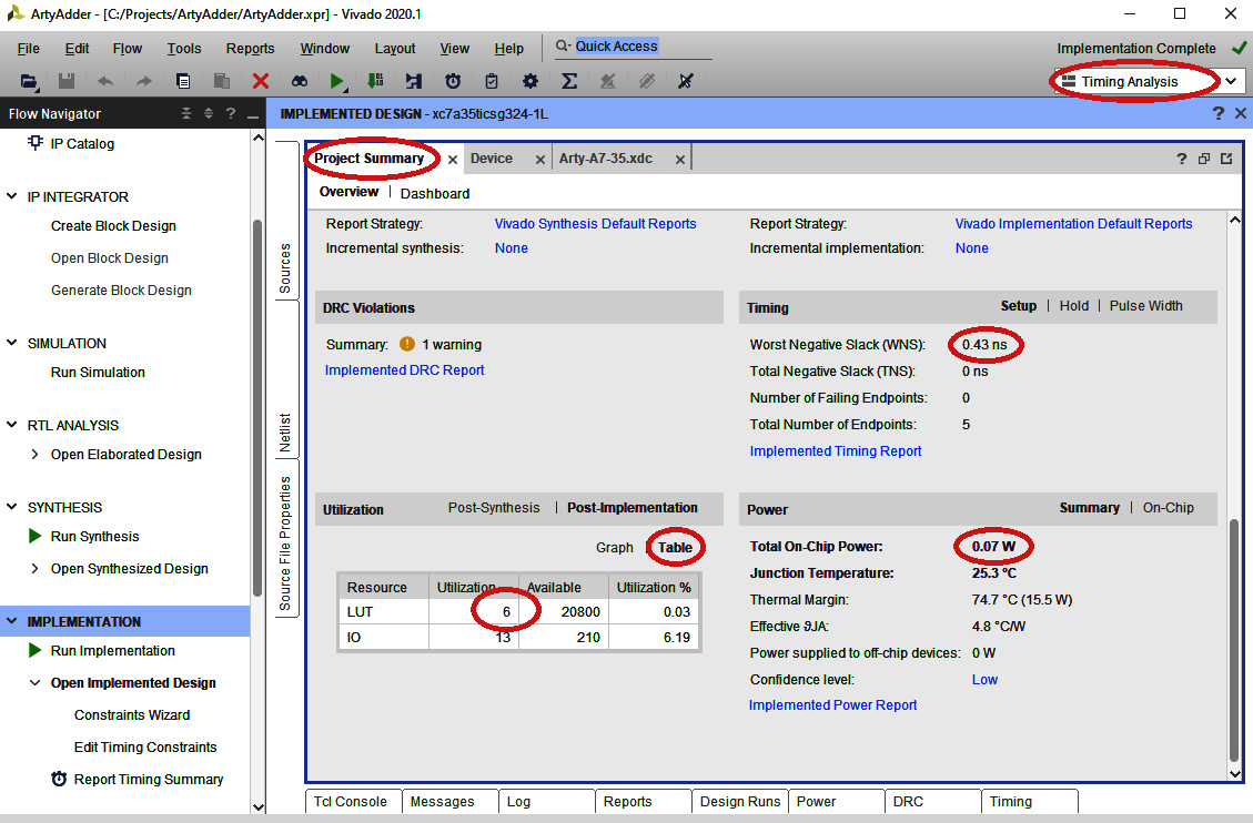
Figure 5.2 – The Timing, Utilization, and Power summaries
This display shows a Worst Negative Slack (WNS) time of 0.43 ns. Numerically, this value represents the most marginal propagation path in the design relative to our maximum delay constraint of 12 ns. Because the WNS is positive, all timing constraints have been met. The actual worst-case propagation delay in the circuit is our constraint (12 ns) minus WNS (0.43 ns), which is 11.57 ns.
The Utilization summary displays the FPGA resource consumption in terms of lookup tables and I/O pins. Click Table to display the number of each item used. Our design consumes 6 LUTs and uses 13 I/O pins (4 switches, 4 buttons, 4 green LEDs, and 1 multicolor LED). The Power summary indicates that our design consumes 0.07 W of power.
If you haven't done so already, add design source files named Adder4LUT.vhdl and Adder4Native.vhdl to your project. Insert the 4-bit adder definition into each file that contains the source code for each model as described earlier in this chapter. For the Adder4LUT.vhdl model, because the code in the case statement is so lengthy and repetitive, you should use your favorite programming language to generate the textual contents of the case statement.
You can switch your implementation of the adder between these three designs by changing two lines in the ArtyAdder.vhdl file. The following example code shows the architecture section of ArtyAdder.vhdl with the two lines changed to select ADDER4NATIVE as the 4-bit adder implementation:
architecture BEHAVIORAL of ARTY_ADDER is
-- Reference the previous definition of the 4-bit adder
component ADDER4NATIVE is
port (
A4 : in std_logic_vector(3 downto 0);
B4 : in std_logic_vector(3 downto 0);
SUM4 : out std_logic_vector(3 downto 0);
C_OUT4 : out std_logic
);
end component;
begin
ADDER : ADDER4NATIVE
port map (
A4 => sw,
B4 => btn,
SUM4 => led,
C_OUT4 => led0_g
);
end architecture BEHAVIORAL;
After changing those two lines, rerun the synthesis and implementation, then view the Timing Utilization and Power summaries. The results of this procedure for each of the three adder designs are shown in the following table:

From these results, it is clear that, although these three design variants were based on substantially different approaches to defining the 4-bit addition operation, and they required significantly varying amounts of source code, the optimized form of each resulted in very similar FPGA implementations in terms of performance and resource utilization.
The key takeaway from this analysis is that developers should not exert substantial effort in attempting to lay out an overly complex, fully optimized design. Instead, create a design that is understandable, maintainable, and functionally correct. Leave the optimization to the compilation tools. They are very good at it.
The next section introduces an alternative method for design entry: high-level synthesis.
High-level synthesis
Our examples up to this point have consisted of VHDL code-based circuit designs. As discussed in the FPGA implementation languages section of Chapter 4, Developing Your First FPGA Program, it is also possible to implement FPGA designs using traditional programming languages such as C and C++.
Although other languages are available for use in high-level synthesis, our discussion will focus on C and C++. The high-level synthesis tools from Xilinx are available within an integrated development environment named Vitis HLS. If you installed Vitis along with Vivado, you can start Vitis HLS by double-clicking the icon with that name on your desktop.
Although most of the capabilities of the C and C++ languages are available in Vitis HLS, there are some significant limitations you must keep in mind:
- Dynamic memory allocation is not allowed. All data items must be allocated as automatic (stack-based) values or as static data. All features of C and C++ that rely on the use of heap memory are unavailable.
- Library functions that assume the presence of an operating system are not available. There is no file reading or writing, and no interaction with users via the console.
- Recursive function calls are not allowed.
- Some forms of pointer conversion are prohibited. Function pointers are not allowed.
One important feature that is available in Vitis HLS that is not available natively in standard C/C++ is support for arbitrary precision integers and for fixed-point numbers. Fixed-point numbers are integers that can represent fractional values by placing the decimal point at a fixed location within the data bits. For example, a 16-bit fixed-point number with the decimal point placed before the two least significant bits has a fractional resolution of ¼. In this format, the number 4642.25 is represented by the binary value 01001000100010.01.
To gain some familiarity with high-level synthesis, let's implement our 4-bit adder in C++ within Vitis HLS. To do so, follow these steps:
- Double-click the Vitis HLS icon to start the application.
- Click Create Project in the Vitis main dialog.
- Name the project ArtyAdder4HLS and set the location to C:Projects as shown in the following figure. Click Next:
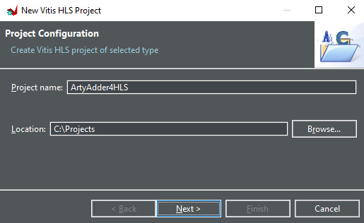
Figure 5.3 – Vitis HLS project configuration dialog
- Set Top Function to ArtyAdder4HLS as shown in the following figure, then click Next:
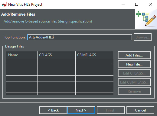
Figure 5.4 – Vitis HLS Add/Remove Files dialog
- Click Next to skip past the Add/remove C-based testbench files dialog.
- Set Solution Name to ArtyAdder4HLS as shown in the following figure, then click Finish:
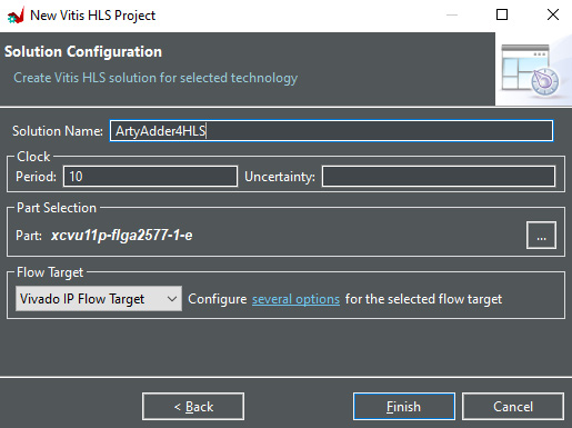
Figure 5.5 – Vitis HLS solution configuration dialog
- In the Vitis Explorer sub-window, right-click Source and select New File…. Enter the name ArtyAdder4HLS.cpp and store it at C:ProjectsArtyAdder4HLS.
- Insert the following code into the ArtyAdder4HLS.cpp file:
#include <ap_int.h>
void ArtyAdder4HLS(ap_uint<4> a, ap_uint<4> b,
ap_uint<4> *sum, ap_uint<1> *c_out)
{
unsigned sum5 = a + b;
*sum = sum5;
*c_out = sum5 >> 4;
}
- The data types identified as ap_uint<> are arbitrary-precision unsigned integers with the number of bits indicated between the angle brackets. Observe that the C++ statements in the body of the function closely mirror the statements in the Adder4Native version of the 4-bit adder.
- Click the green triangle in the icon ribbon to start the synthesis process. If prompted, answer Yes, you want to save the editor file.
Vitis HLS will generate both Verilog and VHDL versions of the model. Expand the ArtyAdder4HLS folder in the Vitis Explorer and double-click the ArtyAdder4HLS.vhd file to open it in the editor as shown in the following screenshot:
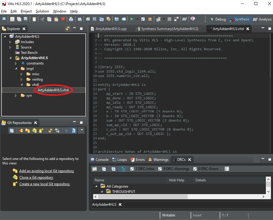
Figure 5.6 – ArtyAdder4HLS.vhd file contents
Vitis HLS adds a control input (ap_start) and status outputs (ap_done, ap_idle, sum_ap_vld, and c_out_ap_vld) to the list of inputs and outputs we have defined for the 4-bit adder. Those signals are not relevant for our circuit, which contains purely combinational logic.
Copy the ArtyAdder4HLS.vhd file to the folder containing the VHDL files for our ArtyAdder project (C:ProjectsArtyAdderArtyAdder.srcssources_1 ew). Add that file to the project and create a new file named ArtyAdder4HLSWrapper.vhdl with the following content:
-- Load the standard libraries
library IEEE;
use IEEE.STD_LOGIC_1164.ALL;
use IEEE.NUMERIC_STD.ALL;
-- Define the 4-bit adder inputs and outputs
entity ADDER4HLSWRAPPER is
port (
A4 : in std_logic_vector(3 downto 0);
B4 : in std_logic_vector(3 downto 0);
SUM4 : out std_logic_vector(3 downto 0);
C_OUT4 : out std_logic
);
end entity ADDER4HLSWRAPPER;
-- Define the behavior of the 4-bit adder
architecture BEHAVIORAL of ADDER4HLSWRAPPER is
component ARTYADDER4HLS is
port (
AP_START : in std_logic;
AP_DONE : out std_logic;
AP_IDLE : out std_logic;
AP_READY : out std_logic;
A : in std_logic_vector(3 downto 0);
B : in std_logic_vector(3 downto 0);
SUM : out std_logic_vector(3 downto 0);
SUM_AP_VLD : out std_logic;
C_OUT : out std_logic_vector(0 downto 0);
C_OUT_AP_VLD : out std_logic
);
end component;
signal c_out_vec : std_logic_vector(0 downto 0);
begin
-- The carry input to the first adder is set to 0
ARTYADDER4HLS_INSTANCE : ARTYADDER4HLS
port map (
AP_START => '1',
AP_DONE => open,
AP_IDLE => open,
AP_READY => open,
A => A4,
B => B4,
SUM => SUM4,
SUM_AP_VLD => open,
C_OUT => c_out_vec,
C_OUT_AP_VLD => open
);
C_OUT4 <= c_out_vec(0);
end architecture BEHAVIORAL;
Here, we have set the unused input to the ARTYADDER4HLS_INSTANCE component to 1 and set the unused outputs to open, meaning the signals are unconnected.
After completing the implementation of this design, we can augment the table in the Design optimization section to add a row with the parameters for the C++ HLS version of the 4-bit adder:

We see that the C++ version of the 4-bit adder results in the best performance in terms of minimizing propagation delay and minimizing resource usage. This may be surprising if you had assumed that coding directly in HDL would produce a better performing result. Of course, this is a very simple example and it would not be prudent to assume similar results would apply to a very complex design. But they might!
Optimization and constraints
In general, given the large quantity of resources available in a particular model of FPGA, it is possible to implement a particular logic circuit source code definition in a tremendous variety of ways. Although each of these variations will perform the logical functions of the circuit in an identical manner, each implementation will be unique in various aspects. Some configurations will use more of the FPGA resources and some will use less. Some will be faster, in terms of propagation delay and attainable clock speed, and some will be slower. Some will consume more power, and some will consume less. Of all the possible ways a specific circuit might be implemented in a given FPGA, how should the tool select the configuration to implement?
By default, the Vivado tools place the highest priority on optimizing timing by minimizing the propagation time of signals that have the slowest paths. As secondary optimization goals, the area (in terms of FPGA resource usage) will be minimized and power consumption will be minimized. For advanced users, configuration options are available to adjust the relative priority of the optimization goals and to adjust the amount of effort, in terms of execution time, to put into the search for an optimal design. Given the very large number of possible configurations, it is not possible for the tools to evaluate every one of them. In general, the result of the optimization process is a design that may not be the best possible configuration. Instead, the result is a design that meets specifications and is likely to be not very far from the absolute best design in terms of performance metrics.
Practical FPGA designs require constraints on the optimization process. One obvious category of constraints is the selection of I/O pins for signals. By indicating that a particular signal must be connected to a specific I/O pin, the synthesis and implementation processes must then restrict their search to consider only configurations that have that signal connected to the given pin. Every I/O signal used by the FPGA logic must have an I/O pin constraint. These constraints define the interface between the FPGA and external circuitry.
The other primary category of constraints relates to timing. In FPGA designs that implement synchronous sequential logic, proper operation of the circuitry is dependent on the reliable operation of flip-flop-based registers. Flip-flops are clocked devices, meaning they capture the input signal on a clock edge. For the input data to be captured reliably, the input signal must be stable for some period of time before the clock edge and must remain stable for an additional length of time following the clock edge.
Figure 5.7 shows a simplified version of the D flip-flop discussed in Chapter 1, Architecting High-Performance Embedded Systems, along with a timing diagram of the D and Clock inputs to the flip-flop:
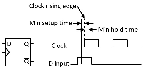
Figure 5.7 – D flip-flop input timing constraints
The flip-flop reads the D signal on the rising edge of the clock. For the flip-flop to read the signal reliably, the input must be at the desired level at least the minimum setup time before the clock edge and it must be held at the same level at least the minimum hold time following the clock edge. In the figure, the D input satisfies the timing constraints and will load a high (binary 1) value into the flip-flop on the first clock rising edge and will load a 0 on the second rising edge.
During the optimization process, the synthesis and implementation tools evaluate the setup and hold time requirements for all synchronous logic elements and attempt to produce a design that satisfies the timing requirements for all devices in the circuit.
If the design is to be connected to an external device with strict timing requirements, or if you know of particular timing constraints internal to the FPGA that the automated tools may not satisfy by default, it is possible to define additional timing constraints to meet the requirements. Basic timing constraints include the clock frequencies used by the FPGA circuit and the setup and hold times of I/O connections to the FPGA. More advanced uses of timing constraints can be employed to declare requirements related to internal communication paths within the FPGA.
An effective FPGA design contains constraint definitions for all of the I/O signal pins in use, including the timing requirements associated with those pins. The constraint set also includes internal timing requirements for the circuit such as clock frequencies used in various portions of the circuit and any other specific timing goals the circuit must satisfy. This information is used by the synthesis and implementation tools in their effort to produce a near-optimal circuit design that satisfies all of the constraints.
With this understanding of the FPGA development process, one of the first things a system architect must consider when developing a new system is whether the use of an FPGA solution even makes sense for that project. To assist with this decision process, the next section describes the types of algorithms that are most suitable for use in FPGA implementations.
Algorithm types most suitable for FPGA implementation
A key differentiating factor of an algorithm suitable for an FPGA-based solution is that data arrives faster than a standard processor, even a high-speed device, can receive the data, perform the necessary processing, and write output to the intended destination. If this is the case for a particular system architecture, the next question to ask is if there is an available off-the-shelf solution that supports the required data rate and is capable of performing the necessary processing. If no such acceptable solution exists, it is prudent to explore the use of an FPGA in the design. The following sections identify some categories of processing algorithms that often involve the use of FPGAs.
Algorithms that process high-speed data streams
Video is an example of a high-speed data source, with high-resolution video arriving at rates of tens of gigabits per second. If your application involves standard video operations such as signal enhancement, frame rate conversion, or motion compensation, it may make sense to use an existing solution rather than developing your own. But if an off-the-shelf video signal processor does not meet your needs, you may want to consider implementing your solution with a custom FPGA design.
Another category of high-speed data stream is produced by high-speed ADCs, with bit rates reaching into the gigabits per second. These ADCs are used in systems such as radar and radio communication systems, among many others. Ordinary processors cannot handle the sheer quantity of data produced by these devices, necessitating the use of an FPGA or another gate array device to perform the initial data reception and processing stages, ultimately generating a lower data rate output for consumption by a processor.
The general approach for using an FPGA in a high-speed data system requires the processing performed by the FPGA to handle the highest-speed aspects of system operation while interaction with the system processor and other peripherals takes place at substantially lower data rates.
Parallel algorithms
Computational algorithms with a high degree of parallelism can be substantially accelerated by execution on an FPGA. The naturally parallel nature of HDLs combines with high-level synthesis capabilities to provide a straightforward path for execution speed acceleration.
Some examples of parallel algorithms that may be suitable for FPGA acceleration include sorting large datasets, matrix operations, genetic algorithms, and neural network algorithms.
If you have an existing software algorithm containing parallel features, it may be possible to generate an FPGA implementation with substantially improved performance by compiling the code using high-level synthesis tools. This approach requires that the algorithm is in a programming language supported by the high-level synthesis tools. A complete system design might implement the accelerated FPGA-based algorithm as a coprocessor running alongside a standard processor that performs all of the remaining work of the system.
Algorithms using nonstandard data sizes
Processors typically operate natively on data sizes of 8, 16, 32, and sometimes 64 bits. When working with devices that produce or receive data in other sizes, for example, a 12-bit ADC, it is common to select the next larger supported data size (in this case, 16 bits) and simply ignore the extra bits appended to the actual data bits.
While this approach is acceptable for many purposes, it also results in the waste of 25% of memory storage space and communication bandwidth when working with these data values unless additional steps are taken to break up the data values and store them in system-supported 8-bit chunks.
Wouldn't it be nice if you could declare variables with a 12-bit data type natively in the software that runs on your system processor? You can't do that in general, but you can define a 12-bit data type in your FPGA model and use that type for data storage, transfer, and mathematical operations. Variables of this data type will only need to be organized into 8-bit chunks, or some multiple of 8 bits, when communicating with external devices.
This section summarized some of the types of algorithms that are candidates for acceleration by implementation in an FPGA. The examples mentioned here are by no means exhaustive. A system designer should consider the use of an FPGA in any scenario where computational throughput is a bottleneck.
In the next section, we will take all of the knowledge we have gained on the use of FPGAs in high-performance embedded systems and focus on a specific project that puts this knowledge to use: a high-speed, high-resolution, digital oscilloscope.
Kicking off the oscilloscope FPGA project
In this section, we will roll up our sleeves and get to work on an FPGA design project that will require the use of the FPGA development process discussed to this point, as well as a high-speed circuit board design, which we will get started on in the next chapter.
Project description
This project will develop a digital oscilloscope based on the Arty A7-100T board that uses a standard oscilloscope probe to measure voltages on a system under test. The key requirements of this project are as follows:
- The input voltage range is ±10V when using a scope probe set to the 1X range.
- The input voltage is sampled at 100 MHz with 14 bits of resolution.
- Input triggering is based on the input signal rising or falling edge and trigger voltage level. Pulse length triggering is also supported.
- Once triggered, up to 248 MB of sequential sample data can be captured. This data will be transferred to the host PC for display after each capture sequence completes.
- The hardware consists of a small add-on board that we will design and construct in the following chapters, which will be plugged into the connectors on the Arty A7-100T development board. The Arty provides the FPGA device used in the system. The add-on board contains the ADC, oscilloscope probe input connector, and analog signal processing.
- After each sample sequence is collected, the Arty transfers the collected data to a host system over Ethernet.
This may seem to be an unusual combination of features, so I will try to provide a rationale for these requirements. The primary purpose of this example is to demonstrate architecture and development techniques for high-performance FPGA-based solutions, not to produce a product that sells well. If you work through and understand the processes used to develop this system, you should be able to move on to other high-performance FPGA designs with ease.
The oscilloscope sampling speed (100 MHz) is not especially fast for a digital oscilloscope. The reason for keeping the speed of ADC sampling at this level is, first, to keep the cost of the parts down. Extremely high-speed ADCs are very costly. The ADC used for this design costs about $37. Second, high-speed circuit design is difficult. Extremely high-speed circuit design is even more difficult. We are only trying to provide an introduction to the issues associated with high-speed circuit design with this project, so limiting the maximum circuit frequency to a reasonable level will help prevent frustration.
The use of the Ethernet communication mechanism opens this architecture up for use as an IoT device. Most digital oscilloscopes use USB to connect to a physically nearby host. With our Ethernet connection, the oscilloscope and its user interface could potentially be on opposite sides of the earth.
The remainder of this chapter sets up a baseline Vivado design for this project.
Baseline Vivado project
This project will use a Xilinx MicroBlaze soft processor running the FreeRTOS real-time operating system to perform TCP/IP communications over the Ethernet port on the Arty A7-100. To complete this phase of the project, you will need the following items:
- An Arty A7-100T board
- A USB cable connecting the Arty board to your computer
- An Ethernet cable connecting the Arty board to your local network
- Vivado installed on your computer
I am assuming you are now a bit familiar with Vivado. Screenshots will only be provided to demonstrate features that have not been seen as part of previous examples.
The following bullet points provide an overview of the steps we will perform:
- Create a new Vivado project.
- Create a block diagram-based representation of a MicroBlaze microcontroller system with interfaces to the following components on the Arty A7 board: DDR3 SDRAM, an Ethernet interface, 4 LEDs, 4 pushbuttons, 4 RGB LEDs, 4 switches, the SPI connector (J6 on the Arty A7 board), and the USB UART.
- Define a 25 MHz clock as the reference clock for the Ethernet interface. This clock signal is assigned to the appropriate pin on the FPGA package using a constraint.
- Generate a bitstream from the design.
- Export the project from Vivado into the Vitis software development environment.
- Create a Vitis project that implements a simple TCP echo server.
- Run the software on the Arty board and observe messages sent via the UART.
- Use Telnet to verify the TCP echo server is working.
Let's get started:
- Begin by creating a project using the steps listed in the Creating a project section in Chapter 4, Developing Your First FPGA Program. The suggested name for this project is oscilloscope-fpga and the location is C:Projectsoscilloscope-fpga.
- Click Create Block Design to open the block design window. You will be prompted for a design name. The default, design_1, is acceptable:
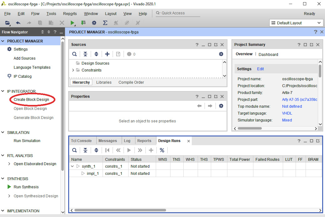
Figure 5.8 – Creating the block design
- Select the Board tab in the Block Design window. Drag System Clock onto the Diagram window.
- Double-click the Clocking Wizard component to open its Re-customize IP dialog. Be sure to double-click the background of the component and not on one of the pin names.
- Select the Output Clocks tab in the dialog. Check the checkboxes next to clk_out2 and clk_out3 (clk_out1 should already be checked). Set Output Freq for clk_out1 to 166.66667 MHz, clk_out2 to 200 MHz, and clk_out3 to 25 MHz:
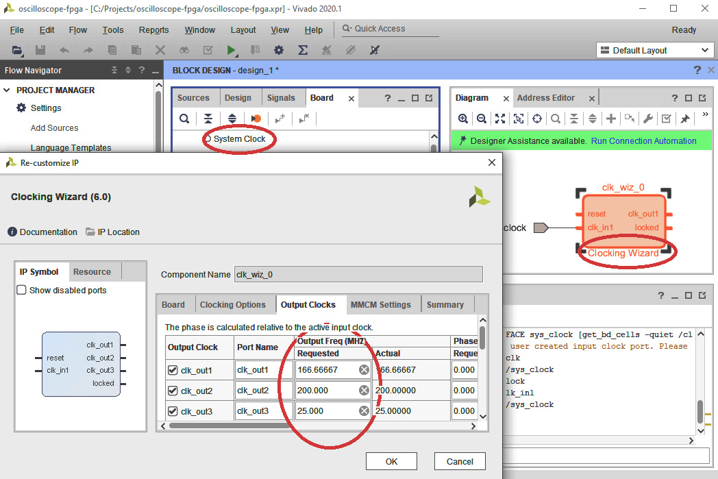
Figure 5.9 – Configuring the Clocking Wizard
- Scroll the Output Clocks window to the bottom and set Reset Type to Active Low. Click OK.
- On the Clocking Wizard component, right-click clk_out3 and select Make External from the menu. A port will appear on the diagram.
- Click on the text clk_out3_0 in the Diagram window. In the External Port Properties window, rename clk_out3_0 to eth_ref_clk.
- Click Run Connection Automation in the green bar. Click OK in the dialog that appears.
- Drag DDR3 SDRAM from the Board tab into the Diagram window.
- Delete the clk_ref_i and sys_clk_i external ports from the Memory Interface Generator (click to select each port, then press the Delete key).
- Click and drag from the clk_out1 pin on Clocking Wizard to the sys_clk_i pin on the Memory Interface Generator to create a connecting wire.
- Click and drag from the clk_out2 pin on the Clocking Wizard to the clk_ref_i pin on the Memory Interface Generator to create a connecting wire.
- Place the mouse over the reset port connected to the Clocking Wizard and when it appears as a pencil, click and drag to the sys_rst input on the Memory Interface Generator. This will create another connecting wire. After this step, the diagram should appear as follows:
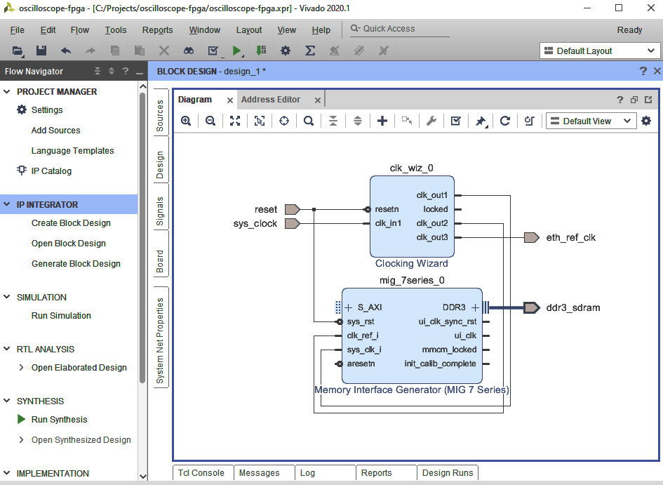
Figure 5.10 – The completed clocking configuration
- Click the + icon at the top of the Diagram window and type micro in the search box that appears. Select the MicroBlaze entry and press Enter.
- Click Run Block Automation in the green bar. Select Real-time as the Preset, set Local Memory to 32 KB, and set Clock Connection to /mig_7series0/ui_clk (83 MHz). Click OK.
- Click Run Connection Automation in the green bar. In the dialog that appears, check the box next to All Automation and click OK.
- Double-click the MicroBlaze component in the diagram. Step through the numbered pages in the dialog and make the following changes: On Page 2, uncheck Enable Integer Divider and Enable Additional Machine Status Register Instructions, and check Enable Branch Target Cache. On Page 3, do not make any changes. On Page 4, set the Instruction and Data Cache sizes both to 32 kB. On Page 5, set Number of PC Breakpoints to 6. No changes are needed on Page 6. Click OK.
- Drag the following items from the Board window into the Diagram window and click OK after adding each one: Ethernet MII, 4 LEDS, 4 Push Buttons, 4 RGB LEDs, 4 Switches, SPI connector J6, and USB UART.
- Click the + icon at the top of the Diagram window and type timer in the search box that appears. Select the AXI Timer entry and press Enter.
- Click Run Connection Automation in the green bar. In the dialog that appears, check the box next to All Automation. Click OK.
- Find the Concat block on the diagram and double-click it to open the Re-customize IP dialog. Change Number of Ports to 3 and click OK.
- Connect the In0-In2 ports of the Concat block to the following pins, in order: AXI EthernetLite/ip2intc_irpt, AXI UartLite/interrupt, and AXI Timer/interrupt.
- Press Ctrl + S to save the design.
- Press F6 to validate the design. Ensure validation is successful with no errors.
- Select the Sources tab in the Block Design window. Right-click on design_1 under Design Sources and select Create HDL Wrapper. Click OK.
This completes the block diagram for the initial phase of the project. In the next series of steps, we will add constraints to specify the characteristics of the Ethernet interface clock output pin:
- Still in the Sources tab, expand Constraints, then right-click on constrs_1 and select Add Sources.
- In the Add Sources dialog, click Next, then click Create File. Name the file arty and click OK, then click Finish.
- Expand the constrs_1 item and double-click arty.xdc to open the file.
- Insert the following text into arty.xdc:
set_property IOSTANDARD LVCMOS33 [get_ports eth_ref_clk]
set_property PACKAGE_PIN G18 [get_ports eth_ref_clk]
- Press Ctrl + S to save the file.
Design entry is now complete for this phase of the project. We will now perform the synthesis, implementation, and bitstream generation steps:
- Under Flow Navigator, click Generate Bitstream. Click Yes in the No Implementation Results Available dialog and OK in the Launch Runs dialog. This process may take several minutes to complete.
- When the Bitstream Generation Completed dialog appears, click Cancel.
If there are no errors reported, this completes the first stage of the oscilloscope FPGA development project. Although we have not implemented any logic related to our ADC interface yet, the current design is capable of booting and running a software application.
Follow these steps to create and run the code for the TCP echo server:
- In Vivado, select File | Export | Export Hardware…. Select the Fixed Platform type, then click Next.
- In the Output dialog, select the Include Bitstream option and click Next.
- In the Files dialog, select the directory C:/Projects/oscilloscope-software and click Next. Click Finish to complete the export.
- Locate the desktop icon titled Xilinx Vitis 2020.1 (or look for your version number, if different) and double-click it.
- Select the C:Projectsoscilloscope-software directory for your workspace and launch Vitis:
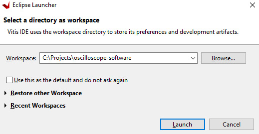
Figure 5.11 – Vitis workspace selection dialog
- In the Vitis main window, click Create Application Project.
- Click Next in the Create a New Application Project window.
- In the Platform dialog, click the Create a new platform from hardware (XSA) tab.
- Click the Browse… button and locate the hardware definition file. This should be at C:Projectsoscilloscope-software design_1_wrapper.xsa. After selecting the file, click Next in the Platform dialog.
- On the Application Project Details screen, enter oscilloscope-software as the Application project name and click Next.
- In the Domain dialog, select freertos10_xilinx in the Operating System dropdown. Click Next.
- In the Templates dialog, select FreeRTOS lwIP Echo Server and click Finish.
- After Vitis finishes setting up the project, it is necessary to change a configuration setting for the Ethernet interface or the application will not work properly. Click Navigate to BSP Settings as shown in the following screenshot:
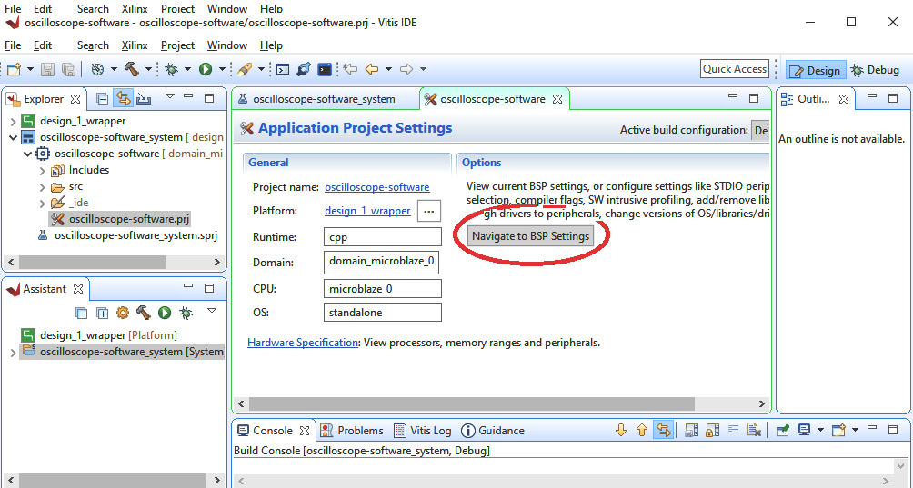
Figure 5.12 – Navigate to BSP Settings button
- In the Board Support Package window, click Modify BSP Settings…, then select lwip211 in the tree on the left. Find the temac_adapter_options section in the main window and expand it. Change phy_link_speed to 100 Mbps (CONFIG_LINKSPEED100) and click OK. This step is necessary because auto-negotiation of link speed does not work properly:
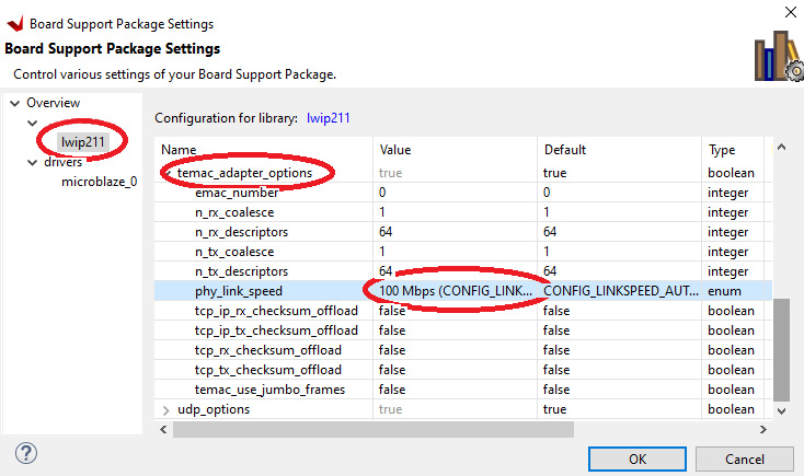
Figure 5.13 – Configuring Ethernet link speed
- Type Ctrl + B to build the project.
If the build process completes with no errors, the result is an executable file that will run on the soft processor in the Arty FPGA. Follow these steps to run the program in the debugger:
- Connect the Arty A7 board to your PC with a USB cable and use an Ethernet cable to connect the Arty Ethernet port to the switch used by your PC.
- Use the Windows Device Manager to identify the COM port number of the Arty board. To do this, type device into the Windows search box and select Device Manager. Expand the Ports (COM and LPT) section. Observe the COM port number that disappears and reappears when you disconnect and reconnect the Arty board USB cable.
- Click the Debug icon in the toolbar as shown in the following screenshot. This will load the configuration bitstream and the application you just built into the FPGA:
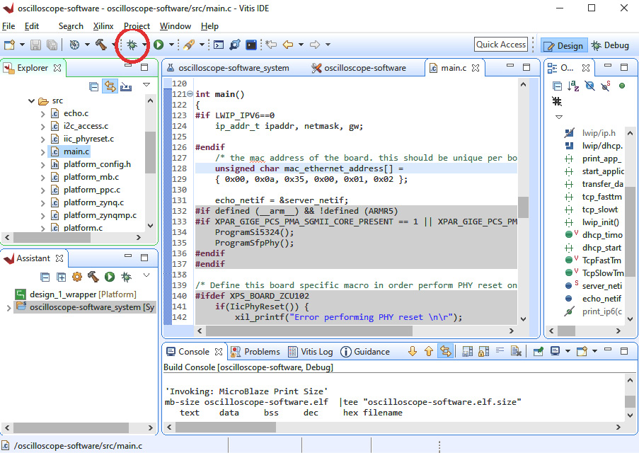
Figure 5.14 – Starting the debugger
- In the bottom-center dialog area, locate the Vitis Serial Terminal tab and click the green + icon to add a serial port:
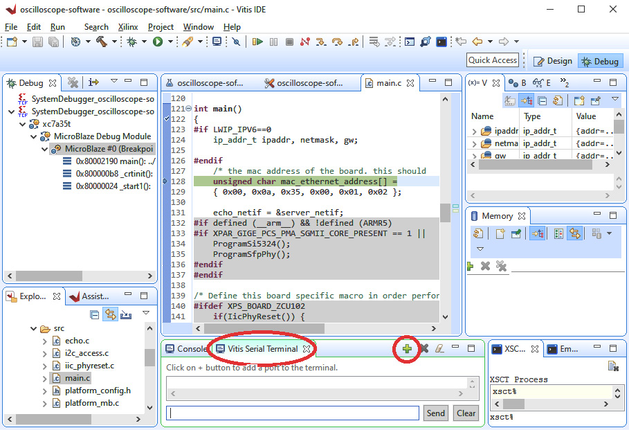
Figure 5.15 – Configuring the serial terminal
- In the Connect to serial port dialog, select the COM port number you identified in the Windows Device Manager and set Baud Rate to 9600. Click OK.
- Press F8 to start the application. You should see output in the serial terminal window similar to this:
-----lwIP Socket Mode Echo server Demo Application ------
link speed: 100
DHCP request success
Board IP: 192.168.1.188
Netmask : 255.255.255.0
Gateway : 192.168.1.1
echo server 7 $ telnet <board_ip> 7
- If you do not have telnet enabled on your Windows computer, run Command Prompt as administrator and enter this command:
dism /online /Enable-Feature /FeatureName:TelnetClient
- After the dism command completes, close the Administrator Command Prompt and open a user-level Command Prompt.
- Using the board IP address displayed in the serial terminal window (192.168.1.188 in this example), run telnet with this command:
telnet 192.168.1.188 7
- Begin typing text in the telnet window. For example, typing abcdefgh produces the following output, which contains an echo of each character except the first:
abbccddeeffgghh
- To verify the echoed characters are coming from the Arty board, break the application execution by clicking the Suspend button as shown in the following screenshot:
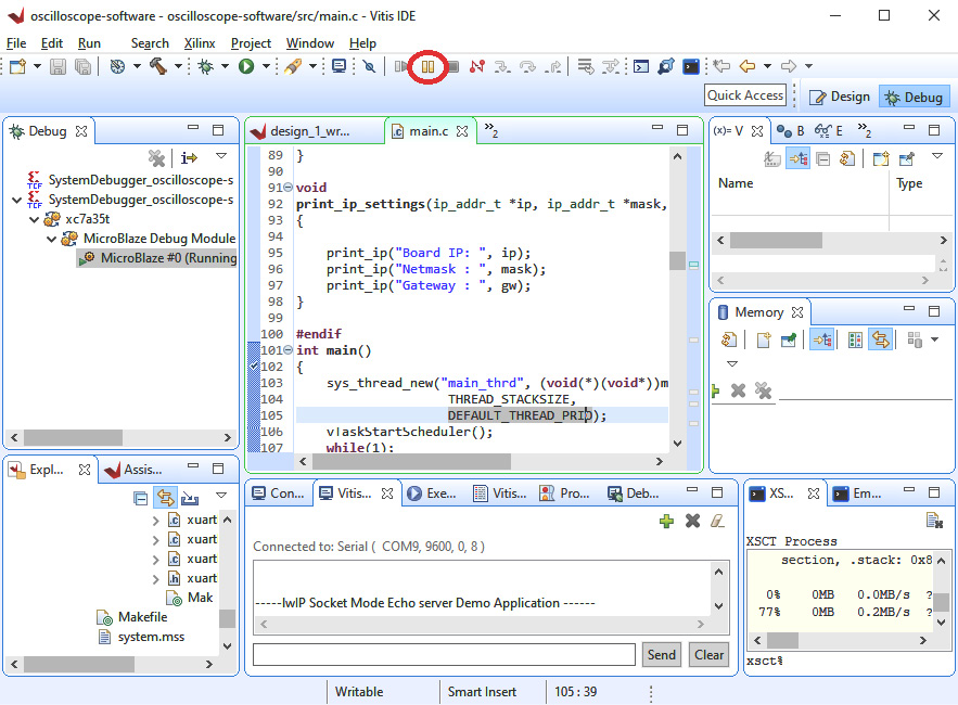
Figure 5.16 – Suspending debugger execution
- Type some more characters into the telnet window. Observe that they are no longer being echoed (only one character appears for each keypress).
This completes the initial implementation phase of the FPGA design and the software application that will run on it. In this chapter, we have developed a baseline Arty A7 MicroBlaze processor system running the FreeRTOS real-time operating system that includes TCP/IP networking.
Summary
This chapter described the process of designing and implementing systems using FPGAs. It began with a description of the FPGA compilation software tools that convert a description of a logic circuit in an HDL into an executable FPGA configuration. The types of algorithms best suited to FPGAs were identified and a decision approach was proposed for determining whether a particular embedded system algorithm is better suited for execution as code on a traditional processor or in a custom FPGA. The chapter concluded with the development of a complete FPGA-based computer system with TCP/IP networking. This project will be further refined into a high-performance network-connected digital oscilloscope in later chapters.
Having completed this chapter, you learned about the processing performed by FPGA compilation software tools. You understand the types of algorithms most suited to FPGA implementation and how to determine whether FPGA implementation is right for a given application. You have also worked through an FPGA design example that will support a high-performance, real-time application in the coming chapters.
The next chapter introduces the excellent, open source KiCad electronics design and automation suite and describes how it can be used to develop high-performance digital circuits. The chapter will continue the example oscilloscope project we began in this chapter, transitioning into the circuit board development phase.