
14
AC–DC converters (rectifiers)
Ahteshamul Haque Department of Electrical Engineering, Faculty of Engineering & Technology, Jamia Millia Islamia University, New Delhi, India
Abstract
Power electronic converters play a major role in renewable energy systems. These converters are used to regulate and shape an electrical signal in the required form. Among these converters, AC–DC converters, commonly known as rectifiers, are used extensively in renewable energy systems such as grid-connected DC microgrids, grid-connected solar photovoltaic energy conversion systems, etc. The main objective of this chapter is to elaborate the working principle of major types of rectifiers. The types discussed are single-phase, three-phase full-bridge controlled, and uncontrolled rectifiers with resistive and inductive load. The workings of these converters are discussed with mathematical expressions and solved examples. The performance parameters are also discussed. Other topics covered in this chapter are pulse width modulated rectifiers and filters for AC–DC converters.
Keywords
single phase
three phase
full bridge
controlled
uncontrolled
filter
PWM (pulse width modulation)
14.1. Introduction
Renewable energy sources need power electronic converters to regulate the power generated and to convert it into a desired shape and quality. Alternating current-to-direct current (AC–DC) converters are a type of power processing converters that are mainly known as rectifiers and are used extensively in renewable energy systems (RES). One such application is the grid-connected DC microgrid [1]. In addition to RES, the use of AC–DC converters is very wide, that is, they are used in drive applications, power quality circuits, etc. It becomes necessary for a power electronics engineer to have a thorough understanding of its working mechanism. The main objective of this chapter is to provide the working of various types of AC–DC rectifiers. AC–DC rectifiers are broadly classified as controlled and uncontrolled rectifiers. They are further classified, based on the AC input supply, that is, single and three phase [2]. The uncontrolled full-bridge rectifier uses diodes as switching devices in applications, where the control of power flow is not required, such as in a constant speed DC drive. However, in controlled rectifiers, switches such as thyristors, IGBT, and MOSFET, are used, which provides the control of power flow [3,4]. In this chapter the working of these two types of converters with resistive and inductive loads, along with their schematics, waveforms, and mathematical expressions have been discussed. Also, in order to evaluate the effectiveness of AC–DC converters, various performance parameters have also been discussed.
The drawbacks of the above rectifiers are poor-power factors and harmonics penetration on the AC side [5]. To overcome this negative effect pulse width modulated (PWM) rectifiers are introduced [6]. The working principle of a PWM rectifier has been explained in this chapter. Details of the filters used in AC–DC rectifiers have also been described. A few solved examples and practice problems are given at the end.
14.2. Performance parameters
Ideally, the magnitude of DC signals should be constant in amplitude and continuous with time. The rectifier is a power processing circuit that converts AC signal into DC signal and should meet the requirements, which is either ideal or close to it. At the same time, a rectifier should maintain the input AC signals that is, current as sinusoidal as possible to maintain the unity power factor. Various types of rectifier circuits used are discussed in the upcoming sections. It is important to evaluate the performance of a rectifier circuit for its closeness towards ideal performance.
The performance parameters used to evaluate the rectifier circuit have been discussed further [2].
14.2.1. Performance parameters of the output side
Rectification efficiency of a rectifier, which shows the effectiveness of the rectification process is,
The output DC voltage of a rectifier is composed of two components,
1. The DC value
2. The AC component, that is, ripple.
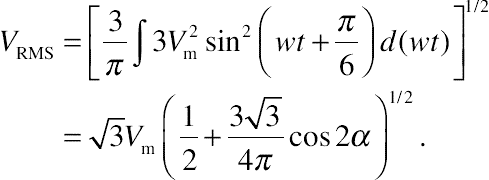
The effective (RMS) value of the AC component of the output voltage is,
 (14.8)
Information about the shape of the output voltage is given by form factor (FF),
The ripple content in the output voltage is measured by ripple factor (RF),
If a transformer is connected at the input side between the AC supply and the rectifier circuit, then the transformer utilization factor is,
where, VS, RMS voltage (secondary) of the transformer supply; IS, RMS current (secondary) of the transformer supply.
14.2.2. Performance parameters of the input side
Let, IS, RMS value of input current; IS1, fundamental component of IS.
If ϕ is the angle between the fundamental component of current and voltage then ϕ is called the displacement angle. The displacement factor is defined as,
The harmonic factor (HF) or total harmonic distortion (THD) of the input current is defined as,
The input power factor PF is,
The crest factor CF is,
Note:
1. If the input current IS is purely sinusoidal, IS1 = IS, then the power factor equals the displacement factor.
2. For an ideal rectifier the values of the parameters are η = 100%, VAC = 0, RF = 0, TUF = 1, HF = THD = 0, PF = DF = 1.
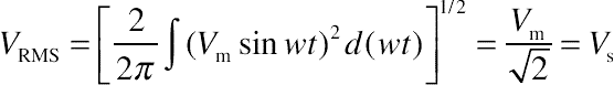
14.3. Single-phase full-bridge rectifier circuit
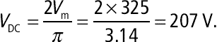
The schematic of a single-phase full-bridge rectifier circuit is shown in Figure 14.1. It has four diodes D1, D2, D3, and D4 connected to an AC voltage source VAC. Diodes D1 and D2 conduct through the load during the positive half cycle of AC voltage supply. Diodes D3 and D4 conduct during the negative half cycle of the AC voltage supply. The AC input voltage VAC can be given directly or through an isolation transformer. The schematic shown in Figure 14.1 is commonly used in practical applications.

Figure 14.1 Schematic of a single-phase full-bridge rectifier circuit.
14.3.1. With resistive load
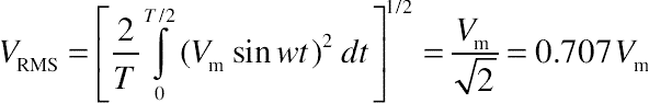
The waveforms with resistive load have been shown in Figure 14.2.
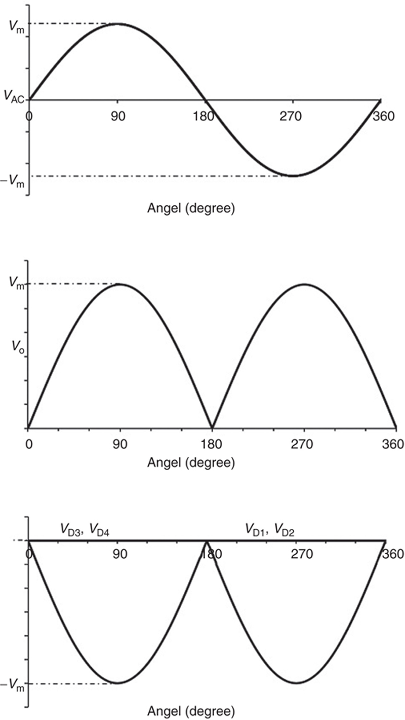
Figure 14.2 Waveforms of a single-phase full-bridge rectifier circuit with R load.
The average output voltage Vo is:
 (14.16)
Since the output voltage is not pure DC and it has AC component in the positive half cycle, it is essential for an engineer to compute the AC component in terms of RMS value.
The RMS value of the output voltage is,
 (14.17)
Example 14.1
In the rectifier circuit of Figure 14.1 the load is purely resistive: R = 100 Ω. The AC input supply voltage is VAC = 325 sin(2π 60t). Calculate (1) the rectification efficiency, (2) the ripple factor, (3) the form factor, (4) the peak inverse voltage (PIV) of diode D1, and (5) the crest factor of the input current.
Solution
The average output voltage is,
The average load current is IDC,
The RMS value of the output voltage is,

RMS load current is,

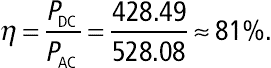
1. The rectification efficiency is,
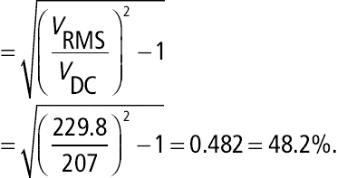
2. The ripple factor is,
3. Form factor = 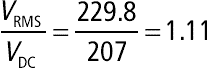
4. The PIV of the diode = Vm = 325 V
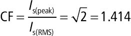
5. The crest factor (CF) of the input current is,
14.3.2. With battery load
Batteries are used in RES to increase reliability. In a grid-connected system, the batteries may be charged from an AC grid via a converter working as a rectifier. In this section the operation of a single-phase full-bridge converter with a battery load is discussed.
The output is connected with a battery as shown in Figure 14.3. If VAC > Vb only, then the current will flow from the AC side via the rectifier circuit to the load.
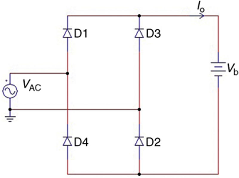
Figure 14.3 Single-phase full-bridge with battery load.
The angle at which the current will start flowing is,
 (14.18)
The current will stop flowing when VAC < Vb,
The charging current Io is,
 (14.19)
R is the internal resistor of the battery connected in series with the battery. The waveforms are shown in Figure 14.4.

Figure 14.4 Waveforms of a single-phase rectifier with battery load.
14.3.3. With highly inductive (R–L) load
In practice, most of the load is inductive in nature. The nature of the load current depends on the value of R and L of the load. An example of highly inductive load is the armature of a DC motor. A schematic of a full-bridge rectifier with R–L load is shown in Figure 14.5.
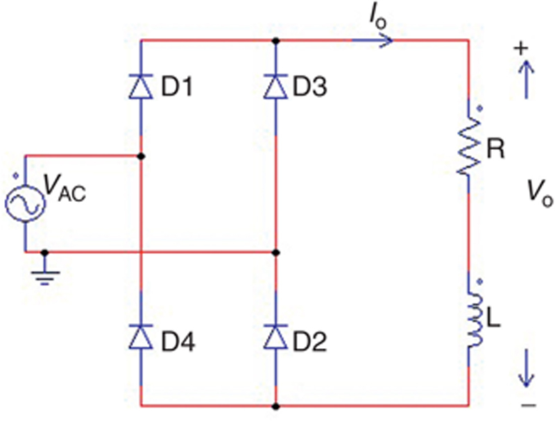
Figure 14.5 Schematic of a full-bridge rectifier circuit with R–L load.
 (14.20)
The waveforms with a highly inductive load are shown in Figure 14.6.

Figure 14.6 Waveforms of a single-phase rectifier with R–L load.
Equation (14.20) has the solution of the form:
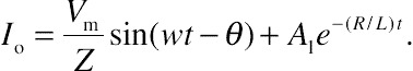 (14.21)
Where load impedance Z = (R2 + (wL)2)1/2 and load impedance angle θ = tan−1(wL/R).
The solution of Equation (14.21) for instantaneous load current will be,
 (14.22)
14.3.4. Fourier analysis
14.3.4.1. Fourier series analysis of DC output voltage
The AC–DC rectifier output voltage may be described by Fourier series analysis as,
 (14.23)

Substituting the values of an and bn, the expression for the output voltage is,
 (14.24)
The output voltage of a single-phase AC–DC rectifier contains only even harmonics and the second harmonic is the most dominant one.
14.3.4.2. Fourier series analysis of AC input current
The input current can be expressed as a Fourier series as shown here,
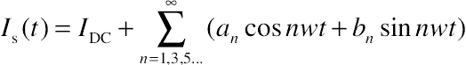 (14.25)
Where,

Substituting the values of an and bn, the expression for the input current is,
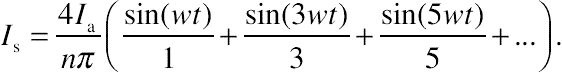 (14.26)
14.4. Three-phase full-bridge rectifier
A three-phase full-bridge rectifier is used in high power applications. This rectifier may work with or without a transformer on the AC supply side. This rectifier gives six pulse ripples on the output voltage in one complete cycle. The numbering of diodes is done as per their sequence of conduction. One diode conducts for 120˚ duration in each cycle and a combination of two diodes conducts for 60˚ in one cycle. The combination of the two diodes conducts when the instantaneous values of AC supply voltages are higher. The load connected at the output may be of two types, that is, resistive (R) load and resistive–inductive (R–L) load. The operation is analyzed in the further sections.
14.4.1. With resistive load
A schematic of a three-phase diode rectifier connected with resistive load R is shown in Figure 14.7. Six diodes, D1–D6, are connected as shown.

Figure 14.7 Schematic of a three-phase bridge rectifier with R load.
The instantaneous phase voltage of AC supply side is,
The line-to-line voltages are,
The average output voltage is,
 (14.33)
The RMS output voltage is,
 (14.34)
If the load is purely resistive, the peak current through the diode is,
 (14.35)
Table 14.1 gives the conduction chart for diodes with line voltages, and the waveforms are given in Figure 14.8.
Table 14.1
Diode conduction chart
| Diodes ON | D5–D6 | D1–D6 | D1–D2 | D3–D2 | D3–D4 | D5–D4 | D5–D6 |
| Line voltages | Vcb | Vab | Vac | Vbc | Vba | Vca | Vcb |
| Duration (angle) | 0–30 | 30–90 | 90–150 | 150–210 | 210–270 | 270–330 | 330–360 |


Figure 14.8 Waveforms of a three-phase bridge rectifier with R load.
14.4.2. With inductive load
The waveforms of the output voltage and current for a three-phase diode bridge rectifier with R–L load are shown in Figure 14.9. The output current has negligible ripples because of its highly inductive nature.

Figure 14.9 Waveforms of a three-phase bridge rectifier with R–L load.
The equation for output voltage remains the same as in the case of R load. The equations for the currents are,
The load current is:
 (14.36)

The RMS diode current is,
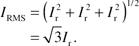 (14.37)
The Fourier series of instantaneous output voltage is,
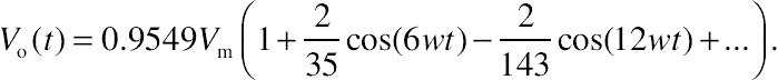 (14.38)
The Fourier series expression for the input current is,
 (14.39)
14.5. PWM rectifier
The diode- and thyristor-controlled rectifier circuits are widely used across industries. These rectifier circuits have a negative impact on the AC supply side as they deteriorate the power quality. The power factor of the AC side goes low. Also, the harmonic content on the AC side current increases. To overcome these drawbacks PWM rectifiers are developed. These rectifiers are designed to operate the switches making power factor either unity or close to unity [5,6].
In this section, a three-phase PWM rectifier is discussed. The circuit of a three-phase voltage source rectifier (VSR), along with its control block diagram, is shown in Figure 14.10.

Figure 14.10 Schematic of a three-phase bridge VSR.
The DC link voltage Vo is fixed at a desired value by using a feedback control signal. It is measured and compared with a reference signal. The error signal controls the ON–OFF states of six switches. The power can flow either to or from the source, depending on the requirement.
In rectifier mode of operation, the load current Io is positive. The error signal demands the flow of power from the AC supply to the load. In the inverter mode the capacitor is overcharged and power flows from the load to AC supply. The control signal decides the power flow by generating an appropriate PWM gate signal.
The PWM rectifier can control both active and reactive power. It is used to correct the power factor, that is, either to unity or close to unity. The AC supply side current is also made close to sinusoidal reducing the harmonic contamination.
The waveforms of the modulation of one phase are shown in Figure 14.11. Figure 14.11a is the PWM signal and Figure 14.11b is the modulating signal.
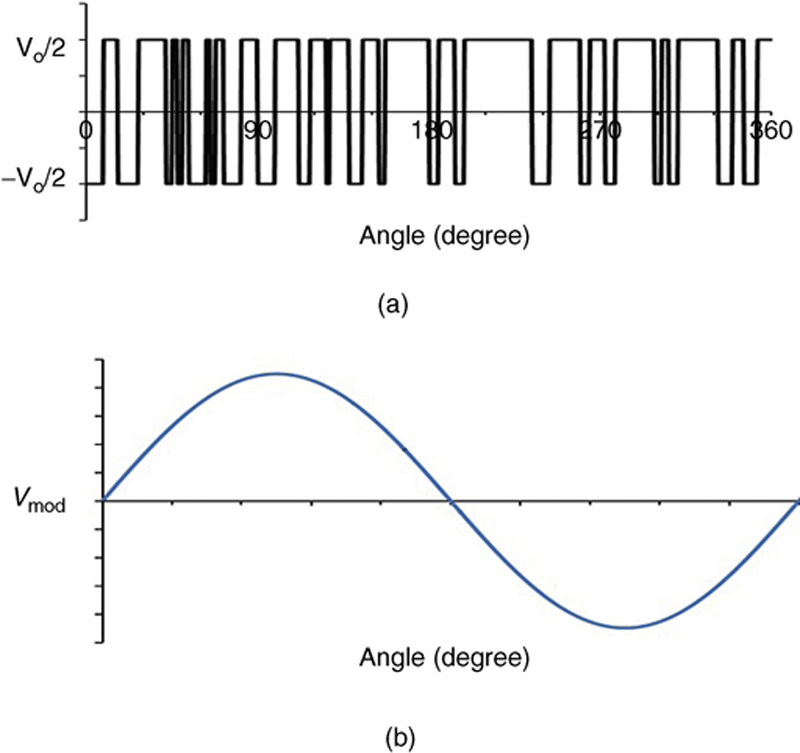
Figure 14.11 Waveforms of PWM three-phase bridge VSR.
(a) PWM and (b) Vmod.
(a) PWM and (b) Vmod.
14.6. Single-phase full-bridge controlled rectifier
The schematic of a single-phase full-bridge rectifier with R–L (highly inductive) load is shown in Figure 14.12. During the positive half cycle of the AC input supply the voltage thyristors T1 and T2 are forward biased and when both thyristors are fired simultaneously at wt = α, load is connected to the input supply through T1 and T2. Since the load is highly inductive, switches T1 and T2 will continue to conduct even when the input voltage goes negative. During the negative half cycle of the AC supply voltage, thyristors T3, T4 are forward biased, and firing T3 and T4 applies the supply voltages across T1 and T2 as a reverse blocking voltage. This will turn off T1 and T2. The load current is transferred to T3 and T4 from T1 and T2. The waveforms of this rectifier are shown in Figure 14.13. Table 14.2 gives the conduction chart for the thyristors.
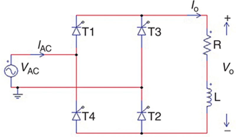
Figure 14.12 Schematic: single-phase full-bridge rectifier.

Figure 14.13 Waveforms: single-phase full-bridge rectifier.
Table 14.2
Thyristor conduction chart
| Thyristor ON | T1–T2 | T3–T4 |
| AC voltages | Positive–negative | Negative–positive |
| Duration (angle) | α to (180 + α) | (180 + α) to (360 + α) |
The average output voltage is,
 (14.40)
RMS value of the output voltage is,
 (14.41)
The output current is,
 (14.42)
Where, Z = (R2+ (wL)2)1/2, θ = tan−1 (wL/R).
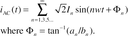
Fourier series expansion of input current is,
 (14.43)
Where,: φn = tan−1(an/bn), and φn = displacement angle of the nth harmonic current.
14.7. Three-phase controlled rectifier
Three-phase rectifiers provide a higher average output voltage compared to single-phase rectifiers. Figure 14.14 shows the schematic of three-phase controlled rectifier connected with highly inductive load. The thyristors are fired at an interval of 60˚. The frequency of the output ripple voltage is 6f (f is the frequency of the AC supply). The filtering requirement is reduced as compared to a single-phase rectifier.

Figure 14.14 Schematic: three-phase full-bridge controlled rectifier with R–L load.
Figure 14.15 shows the waveforms of the AC phase voltages and DC output voltage. Table 14.3 gives a summary of the thyristor switch conduction.
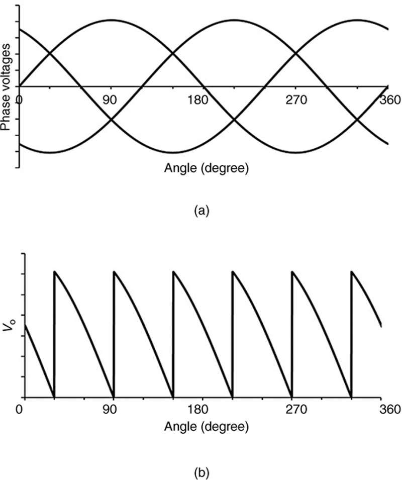
Figure 14.15 Waveforms: three-phase full-bridge controlled rectifier with R–L load.
(a) AC phase voltages and (b) DC output voltage.
(a) AC phase voltages and (b) DC output voltage.
Table 14.3
Summary of the thyristor switch conduction chart
| Thyristors ON | T5–T6 | T6–T1 | T1–T2 | T2–T3 | T3–T4 | T4–T5 | T5–T6 |
| Phase voltages | a, c, b | a, b, c | b, a, c | b, c, a | c, b, a | c, a, b | a, c, b |
| Duration (angle) | (0–30) + α | (30 + α) to (90 + α) | (90 + α) to (150 + α) | (150 + α) to (210 + α) | (210 + α) to (270 + α) | (270 + α) to (330 + α) | (330 + α) to 360 |

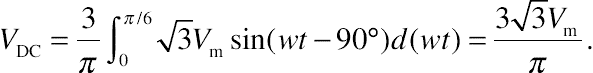
The equations of instantaneous phase and line voltages are,
 (14.44)
The average output voltage is,
 (14.45)
The RMS value of the output voltage is,
 (14.46)
Fourier series of the AC supply side current connected to a highly inductive load via a three-phase full-bridge controlled rectifier is,
 (14.47)
14.8. Filters for AC to DC converters
In rectifier circuits two types of filters are used, that is, one is a DC filter connected at the output to remove the ripple of the DC voltage and other is an AC filter connected at the AC input side to remove the harmonic contents of the AC current. The schematics are shown in Figure 14.16.

Figure 14.16 Schematic representation.
(a) DC filter and (b) AC filter.
(a) DC filter and (b) AC filter.
In most of the applications, a capacitor is used in a DC filter (Figure 14.16a (2)). It gives satisfactory performance.
Figures 14.17 and 14.18 are waveforms of the rectified output voltage with and without a DC capacitor filter.

Figure 14.17 Rectified voltage without DC filter.

Figure 14.18 Rectified voltage with DC filter.
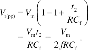
When the voltage across capacitor Cf of the DC filter capacitor is lower than the instantaneous input AC voltage, the Cf will be charged through the rectifier circuit. If the voltage across capacitor Cf is higher than the instantaneous AC input supply voltage then it will discharge through the resistive load. The voltage across Cf will vary. Assuming t1 is the time for charging of Cf, it will charge to the value of the peak supply voltage Vm and t2 is the time for discharging the capacitor Cf as shown in Figure 14.18. The capacitor Cf will be discharged through the resistive load exponentially.
The peak-to-peak ripple voltage Vr(pp) is,
 (14.48)
Since e−x ≈ 1 − x:
 (14.49)
Average output voltage is,
 (14.50)
RMS output ripple voltage Voc is,
 (14.51)
Ripple factor is,
 (14.52)
This expression can be solved to get the value of the filter capacitor Cf.
14.9. Summary
There are different types of rectifiers used in various applications depending on diode connections. These rectifiers are used in RES and in other applications. In this chapter the performance parameters of the rectifiers were defined to evaluate the quality of the rectifiers. The workings of the main types of rectifiers were discussed with schematics, waveforms, and mathematical expressions. The negative effect of the rectifier circuits is harmonics penetration. To overcome this effect PWM rectifiers are used. The other method is to use filter circuits.
..................Content has been hidden....................
You can't read the all page of ebook, please click here login for view all page.