
Chapter 10
Feedback Amplifiers

Equivalent circuit of a current amplifier
Chapter Outline
The concepts introduced in this chapter are:
- Various types of amplifiers and distortion
- Need for feedback in an amplifier
- Types of feedback amplifiers
- Analysis of negative feedback amplifiers
10.1 TYPES OF AMPLIFIERS
Transistor amplifiers can be of various types. The amplifiers are designed to suit a specific requirement. So, amplifiers can be classified under various heads. Classification of amplifiers can be done in many ways. For example, they may be classified based on frequency of operation, type of coupling between the stages, input and output parameters, selection of operating point, method of operation, types of applications, type of load, power delivered to the load, distortion, noise and so on.
Classification of amplifiers based on frequency of operation can be done as follows: dc (zero frequency), audio (20 Hz–20 kHz), video or wideband (few MHz of bandwidth), radio frequency (RF), ultrahigh frequency (UHF), microwave frequency and so on. Amplifiers may also be classified based on the coupling between the stages of the amplifier. The types of the amplifiers possible are RC coupled, direct coupled, transformer coupled and so on. Amplifiers may also be classified as voltage, current, transconductance or transresistance, depending on the input and output parameters. The position of the quiescent point on the load line is also a basis for classifying the amplifier types. It may be class A, class B, class AB or class C. Further, they may be distortionless, low noise, high power, linear, buffer, and many more types.
Classification based on the quiescent point position: If the operating point is selected on the load line in such a way that the output current is available for the complete cycle of the signal, the amplifier is referred to as class A type. In this type, the amplifier operating point is to be selected such that it lies approximately in the mid-region of the load line in the active region. Class A amplifier has the advantage that the signal distortion is at the minimum since the amplifier is operating in linear portion of the load line. In other words, the shape of the signal at the output is almost the same as that of the input with amplification. The limitation of the circuit is that its efficiency is very small, 50% maximum; large amount of input power is wasted in the form of heat. In this type, when the input signal is absent, the transistor continues to draw the same rated power and since the input signal power is not available, all the power is dissipated as heat. So, heat sink should be properly designed to dissipate total dc power drawn by the transistor rather than to dissipate only the excess power when the transistor is in operation. In other words, the transistor is cool when in operation rather than when it is idle.
When the operating point is selected towards one end of the active region on the load line of the transistor amplifier circuit, the signal is available only for 50% of the cycle and is grounded in the other half of the cycle. This type of amplifier is referred to as class B. The current in the output circuit flows only for 50% of the cycle and passing this pulsed current into a tank circuit develops the voltage signal in the output load. The distortion of the signal is large compared to the class A amplifier. The efficiency of the circuit is improved, and is approximately 78% maximum. Selection of the operating point midway between class A and class B has advantage of efficiency over class A and distortion over class B. So, selecting the operating point in such a way that the output current is available between 50% and 100% of the cycle is called class AB. This type of amplifier has the characteristics midway of class A and class B.
Efficiency of the amplifier circuit can be improved even up to 99.99% or more when the operating point is so selected that the current in the output of the amplifier circuit is far less than 50% of the cycle. In this Class C amplifier, the output current is of the form of spikes almost. When these spikes activate the resonant tank circuit, sinusoidal voltage is developed across it. But this signal at the output has lot of harmonics present, which distort the signal to a very large extent. Nonlinearity of the circuit operation is at its peak and so distorts the signal greatly. In this type of amplifier, heat dissipation is minimal since it has very good conversion efficiency. When the input signal is not present, the circuit never draws any current or, in other words, the power dissipated in the form of heat when the transistor in not in operation is zero.
The selection of the type of amplifier depends on the application. One has to compromise either efficiency or distortion. Various circuits are possible which can decrease distortion in the signal to a large extent in class B amplifiers also.
Classification based on the input and output parameter: The possible parameters either at input or output of the amplifier are voltage and current. Not all the amplifiers are of voltage type. They can be classified based on the parameter of interest at the input and output of the amplifier.
If one is interested in voltage both at the input as well as at the output of the amplifier circuit, the amplifier can be named as voltage amplifier. In this type of amplifier, the transfer gain, defined as the ratio of output parameter to that of the input parameter, is voltage gain. Hence, voltage gain AV of an amplifier is the ratio of output voltage to input voltage. The equivalent circuit of the amplifier can thus be easily visualised with Thevenin’s theorem. The equivalent circuit of such an amplifier is as shown in Fig. 10.1. As seen from the circuit diagram, if the amplifier is to have an amplification of AV, the source resistance should be zero or the input impedance of the amplifier should be infinite so that the impressed voltage at the input of the amplifier, vi, will be equal to vs. Both conditions of source impedance being zero or input impedance being infinite are not practicable, the input resistance should be as high as possible as compared to the source resistance. This assures that the drop across the source resistance is very small and loss in the input signal will be at minimum. Looking at the output circuit of the amplifier, if the output impedance of the amplifier is large compared to the load impedance, lot of the signal is lost in this output impedance and so, one requires very low output impedance compared to the load resistance. Ideally, input impedance should be infinite and the output impedance should be zero in a voltage amplifier.
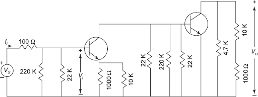
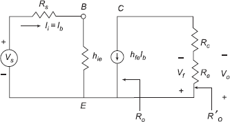
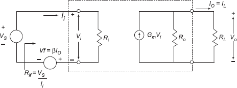
Fig. 10.2 shows the circuit of a current amplifier in which both the input and the output parameter of an amplifier is current. So, the transfer gain of such an amplifier is current gain AI and can be defined as the ratio of output current to the input current. The input and output of the circuit are represented with the help of Norton’s theorem. As seen from the circuit diagram, if the input impedance of the amplifier is very high compared to the source resistance, the current delivered to the amplifier would be very small and so rated current gain cannot be achieved. So, one has to design the current amplifier such that the input impedance should be as small as possible compared to the source resistance. With the same argument extended to output circuit, the output impedance should be as large as possible. Ideally, the current amplifier will have zero input impedance and infinite output impedance.
When the parameter of interest at the input of the amplifier is voltage and that of output is current, the transfer ratio is a ratio of output current to the input voltage, which can be designated as transconductance or mutual conductance GM. The amplifier is referred to as transconductance amplifier. The circuit of such an amplifier, as shown in Fig. 10.3, suggests that both input and output impedance need to be very high compared to that of source and load impedance, respectively. Or, in other words, ideally, the transconductance amplifier has both the input as well as output impedance infinite.


Fig. 10.2 Equivalent circuit of a current amplifier
Transresistance amplifier is that amplifier where the output parameter is voltage and that of input is current. The transfer gain is transresistance RM, which can be defined as the ratio of output voltage to input current. Figure 10.4 shows an equivalent circuit of the transresistance amplifier where both the input and output impedances need to be very small compared to source and load impedances, respectively. Transresistance amplifier has both the impedances zero ideally.
Table 10.1 gives the ideal characteristics of various types of amplifiers along with their transfer ratios.

Fig. 10.3 Equivalent circuit of transconductance amplifier
10.2 TYPES OF DISTORTION IN AMPLIFIERS
The signal given at the input of an amplifier is available at the output of the amplifier after required amplification. This is not sufficient, the shape of the signal is also to be maintained intact. In addition, the signal should not have any other frequency components except those that are fed in the input of the amplifier. This ensures the perfect nature of the amplifier. But this type of amplifier is not practically possible and the shape of the signal is distorted and also additional components of frequency are present in the output of the circuit. The change in shape of the signal at the output of the amplifier is referred to as distortion. Distortion in amplifiers may be due to various sources and can be classified as amplitude, frequency and phase distortion.

Fig. 10.4 Equivalent circuit of a trans resistance amplifier
Table 10.1 Ideal Characteristics of Various Types of Amplifiers

The additional frequency components available in the output of the amplifier can be termed as noise. The noise is the electrical random variations present all over the frequency band from zero to infinity cycles. Noise is present in all the electronic components, active or passive. The electrons, which are present in the device and not contributing to the signal processing, move randomly creating unwanted electrical variations in a device. The frequency of these unwanted electrons’ movement depends randomly on the lifetime of the electron and so, the variations are omnipresent in the total frequency band.
Amplitude distortion: Amplitude distortion, also known as nonlinear distortion, is due to the nonlinearity of the device. The active device employed in the amplification of the signal is either transistor or a FET. Both of these devices are nonlinear. The transfer characteristic of the amplifier, if plotted between input and output parameters of the amplifier, is linear to some extent, whereas it tends towards saturation and the output power does not increase beyond a particular value even though the input increases. This is where the nonlinearity sets in, and distorts the signal. Mainly, such a type of distortion alters the amplitude of the signal and so it is referred to as amplitude distortion. Harmonics are generated in the output by the device and the output contains the harmonics of the basic input frequency components ultimately affecting the amplitude of the signal.
Frequency distortion: The amplification offered by an amplifier is suppose to be uniform throughout the frequency band of interest. If such an amplifier is designed, it does not have any frequency distortion. But, in practice, the amplification offered by an amplifier is not uniform throughout the frequency band of interest. That is, the transfer gain of the amplifier varies with frequency, leading to what is known as frequency distortion. Or, in other words, signal components of different frequencies are amplified differently. This is due to the internal capacitances of the device or due to the associated circuit being reactive. So, the gain of the amplifier is not a scalar quantity, but is complex, having both amplitude and phase. The frequency response of such an amplifier with frequency distortion is not a horizontal straight line.
Phase distortion: Additional phase is introduced into the input of the signal in an amplifier depending on the characteristic of the amplifier. If this additional phase introduced by the amplifier is same for all the frequency components of interest, then the amplifier is not having phase distortion. But, in general, this is not the case and the phase introduced by the amplifier varies with respect to the frequency component of the input signal leading to what is known as phase distortion. This is also once again due to the complex nature of the gain of the amplifier.
10.3 NEED FOR FEEDBACK
The active device used in an amplifier, transistor or FET, has parameters that are not constant. For example, the small signal current gain of a transistor is dependent on ambient temperature at which the device is operating. This variation of parameters of the active device leads to inconsistent nature of the output of the device. If an amplifier is designed using a transistor, the amplification depends on the temperature and increases with temperature and vice versa. This leads to a very unpleasant characteristic of the amplifier that the output is large when the amplifier is operating in a hot condition, but the output is very low when the amplifier is subject to very low temperatures. So, stability of the amplifier is required, that is, the output of the amplifier should be maintained almost constant irrespective of temperature variations. This requires a feedback system where the output of the amplifier is constantly monitored and the input is adjusted accordingly so that the output is constant. In other words, when temperature increases, increasing the gain of the device, the feedback system decreases the input signal level such that the output signal is brought back to approximately the previous value or vice versa. This type of feedback system involving simple passive circuit design is referred to as negative feedback. The negative feedback not only improves the stability of the device, but also improves various parameters of the amplifier. There are quite a large number of advantages of employing negative feedback in the amplifier circuits. The disadvantage of such a system is that the gain of the amplifier decreases.
10.4 NEGATIVE FEEDBACK IN AMPLIFIERS
The feedback employed in an amplifier has very good advantages. Negative feedback in an amplifier involves few more blocks to be added to the basic amplifier. The block diagram of the amplifier employing negative feedback is as shown in Fig. 10.5. The additional circuitry involves sampler at the output of the amplifier, feedback circuit consisting of passive components and a mixer at the input of the amplifier.
The sampler is at the output of the amplifier and it samples the signal of interest and presents it to the feedback circuit. The sampled signal may be voltage or current. If voltage is the signal that is sampled, it is referred to as voltage or node sampling. If current is sampled, it is known as current or loop sampling. The sampling is done in such a way that the output of the amplifier is not loaded and the output signal is tracked properly.
The feedback network is a circuit made up of passive components. Its input is the sample of the output of the amplifier and its output is fed to the input of the amplifier. The circuit processes the output signal from the amplifier and presents this feedback signal to the input out of phase to that of the source signal. The feedback signal may be either voltage or current, depending on series mixing or shunt mixing employed at the input of the amplifier. Since the feedback signal and the source signal are out of phase by 180°, the difference of the signals is presented as the input signal to the amplifier. So, the amplifier amplifies the difference signal but not the source signal. This is the reason why such a type of feedback is referred to as negative feedback.
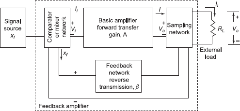
Fig. 10.5 Negative feedback in an amplifier
The mixer, also referred to as comparator, is a circuit that mixes the source signal and the feedback signal from the output of the feedback network out of phase. The mixing can be of two types. If the two are mixed in series, then it is referred to as series or loop mixing. If the mixing is in shunt, then it is shunt or node mixing. The difference of the two signals is presented to the amplifier as the input signal.
The source signal is derived from the source of the signal. This may be, once again, voltage or current. The amplifier is characterised by the type of parameter at the input and output of the amplifier of interest. So, the transfer ratio or gain of the amplifier may be voltage gain, current gain, transconductance or transresistance, depending on the signals of interest.
The first and foremost advantage of the negative feedback is stability. Whatever may the reason, if the output of the amplifier increases, the same increase is applied to the feedback circuit by sampling circuit. The feedback circuit processes the increase in signal and applies the proportionate ratio of the increase to the mixer. The mixer mixes this signal with source signal out of phase, or, in other words, the difference of the source and increased feedback signal is fed to input of the amplifier. Since the feedback signal is large compared to previous case, the input signal is decreased to the extent required. Thus, the output of the amplifier is decreased, compensating for the initial increase in the output signal of the amplifier. Thus, the output is stabilised, that is, maintained almost constant irrespective of variations of any type affecting the basic amplifier parameters. Even though the compensation may not be cent per cent, the output is constantly sampled and the output of the amplifier is maintained almost constant. The same argument can be extended when the output decreases. Decreasing output decreases the feedback signal to the mixer, which in turn increases the input to the amplifier. Thus, increasing the input to the amplifier compensates the decrease in signal at the output of the amplifier. Not only the stability of the amplifier is improved, but also input and output impedances are improved, bandwidth increases, distortion decreases, noise content decreases associated with only one disadvantage that the amplification with feedback decreases. This drawback of the circuit can be overcome easily by designing the amplifier with higher gain than the required value, so that after introduction of the feedback the amplification would be the targeted value.
10.5 TRANSFER GAIN WITH FEEDBACK
The concept of negative feedback as introduced in the previous sections is not true always. There are some assumptions at which the discussion is valid. The assumptions are as follows:
- The signal travels through the amplifier only in forward direction but not in the feedback network. That is, the signal applied from source to input of the amplifier should only pass through the amplifier but should not enter the feedback network. Or, in other words, the feedback network should block the forward signal.
- The feedback signal from the sampler should be only coupled to feedback circuit and the amplifier should not allow the signal to transmit through it in the reverse direction. That is, the amplifier should not be bilateral. It should allow forward signals but not the feedback signals.
- The feedback circuit should not be loaded by either the source or load of the amplifier circuit. In other words, the transfer ratio of the feedback circuit should be independent of source and load impedances.
In a negative feedback amplifier configuration, since sampling can be either voltage or current, and mixing can be either in shunt or series, different types of feedback amplifiers can be evolved depending on the sampling and mixing. So, the feedback amplifiers can be broadly classified as voltage series, current series, current shunt and current series feedback amplifiers.
If voltage is sampled and the mixing is in series in an amplifier, then the type of feedback is referred to as voltage series. Since voltage is sampled, the output parameter of the amplifier monitored is voltage and since the mixing at the input is series type, the parameter that is affected at the input of the amplifier is also voltage. So, voltage is the parameter at the input that is affected and voltage is the parameter at the output that is sampled. So, the parameter that is stabilised in this configuration of feedback is voltage gain AV. So, when voltage series feedback is employed in an amplifier, the parameter stabilised is voltage gain. The transfer ratio β, known as reverse transmission factor, of the feedback is defined as the ratio of output signal to the input signal of the feedback network, that is, ratio of feedback signal to the output signal of the amplifier, Xf/Xo. Then, the transfer ratio of the voltage series feedback amplifier will be the ratio of feedback voltage Vf and the output voltage of the amplifier Vo, or β = Vf/Vo. The schematic of such an amplifier is as shown in Fig. 10.6(a).

Fig. 10.6 Types of feedback amplifiers
In a current series feedback amplifier, the parameter that is sampled at the output of the amplifier is current and the mixing at the input is in series. Since current is sampled, and the mixing is in series, the parameter at the output is current and that at the input is voltage. So, the parameter of the amplifier that is stabilised is transconductance GM. The transfer ratio of the feedback network in this configuration has the ratio of voltage to current, that is, β = Vf/Io. The block diagram of such a configuration is as shown in Fig. 10.6(b).
Figure 10.6(c) shows one more configuration of feedback amplifier, current shunt. In this configuration, the parameter that is sampled is current and mixing at the input of the amplifier is shunt. Since mixing is shunt, the parameter that is affected is current and so, the parameter that is stabilised is current gain AI. The transfer ratio of feedback circuit can be given as the ratio of feedback current to output current, β = If/Io.
The parameter of the amplifier which is stabilised in a voltage shunt feedback amplifier is transresistance RM, since the sampled signal is voltage and mixing is shunt. As the schematic for such a configuration shown in Fig. 10.6(d) suggests, the transfer ratio β of the feedback is ratio of feedback current to output voltage, that is, β = If/Vo.
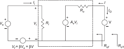
A general schematic of the negative feedback amplifier is as shown in Fig. 10.7. In this, X represents the signal; it can be either voltage or current depending on the configuration of the circuit. So, Xs represents the source signal, Xi the input signal to the amplifier, Xo the output signal of the amplifier and Xf the feedback signal. Since the input to the amplifier is the source and feedback signals added out of phase,
Basic amplifier transfer ratio is given as
Transfer ratio of the feedback network is

Fig. 10.7 Feedback amplifier
Therefore, transfer ratio of the amplifier with feedback can be expressed as
or, from Eq. (10.1),
Dividing the numerator and denominator by Xi
or

A in the above equation represents the transfer gain of the amplifier without feedback, but including the loading of β, RL and Rs.
If ∣Af∣< ∣A∣, the feedback is termed as negative or degenerative and if ∣Af∣>∣A∣, the feedback is referred to as positive or regenerative. For a negative feedback, it is observed that Af is small compared to the basic amplifier transfer ratio or ∣1 + Aβ∣ is greater than unity.
Starting at the input of the amplifier, the signal Xi is first multiplied by A and then by β and next by −1 to land at the same point in the closed loop in the feedback amplifier. Therefore the product − Aβ is called loop gain or return ratio. The difference between 1 and loop gain is referred to as return difference, D = 1 + Aβ. The amount of feedback introduced into the amplifier is expressed in decibels as
|
N = dB of feedback = 20 log ∣(Af/A)∣ |
|
= 20 log ∣1/[1 + Aβ]| …(10.8) |
N will be negative for degenerative feedback and positive for regenerative feedback circuits.
10.6 ADVANTAGES AND DISADVANTAGES OF NEGATIVE FEEDBACK
Use of negative feedback in an amplifier has lot of advantages and the only disadvantage is that the transfer gain of the amplifier is reduced. The following are the major advantages of employing negative feedback in an amplifier.
Desensitivity of transfer gain: As already discussed in the previous sections, the stability of the amplifier is improved to a very large extent by employing negative feedback in an amplifier. Or, in other words, the amplifier is made insensitive to any external variations. The output signal is stabilised and made constant irrespective of variations of any nature. To be more specific, the amplifier is desensitized and now the desensitivity of the amplifier is a measure of ability of the amplifier to maintain its output constant due to variations because of ageing, temperature, replacement and so on of the circuit components. The sensitivity of the amplifier can be expressed as the ratio of fractional change in amplification with feedback to the fractional change without feedback. The same can be expressed as

or, sensitivity is 1/[1 + Aβ] and reciprocal of sensitivity is desensitivity. Hence,
Therefore, transfer with feedback can be given as
and if ∣Aβ∣ ≫ 1,
which shows that the gain of the amplifier entirely depends on the feedback network and if the network contains only passive components, the stability of the amplifier is very pronounced.
Since A represents transfer gain without feedback and Af represents transfer gain with feedback, the parameter that is stabilised depends on the type of feedback employed in the circuit. If voltage series feedback is employed in the circuit, the parameter stabilised is voltage gain and so, Eq. (10.11) can be written as
For an amplifier, all the four parameters can be measured and employing one particular feedback in the circuit stabilises the corresponding parameter of the amplifier. It is not that other parameters of the amplifier are not effected by the feedback, but they are altered and extent of change in those parameters should be only determined with the analysis of the amplifier circuit.
Similarly, employing current series feedback, current shunt feedback and voltage shunt feedback in the amplifier circuits, the parameters of the amplifier that are stabilised are transresistance, current gain and transconductance, respectively.
So, if one desires an amplifier with gain of A and desensitivity D, then he will have to design an amplifier with gain AD and desensitivity D to achieve the required gain as well as stability.
Frequency distortion: Considering Eq. (10.12), it can be easily seen that the amplifier response is independent of frequency. Under these circumstances a substantial reduction in frequency and phase distortion is obtained. It most practical cases it can be generalised that the distortion is reduced by a factor of desensitivity D with feedback.
If the feedback circuit is reactive, being frequency selective, β depends on frequency and so amplification may depend upon frequency. It is possible to obtain an amplifier with high Q band pass characteristic by using a feedback network that gives little feedback at the centre frequency and great deal of feedback at the edges of the frequency.
Amplitude or nonlinear distortion: The distortion due to nonlinearity of the amplifier affects amplitude at the output of the amplifier and generates harmonics. Harmonic distortion is defined as the ratio of amplitude of that particular harmonic amplitude to that of the fundamental. This harmonic distortion is decreased by a factor of desensitivity D with negative feedback in an amplifier. If B2 is second-harmonic distortion without feedback and B2f is the second-harmonic distortion with feedback, then
where D = 1 + Aβ, A and β to be evaluated at the second-harmonic frequency since both are functions of frequency.
Noise: The amount of noise introduced by the amplifier is divided by desensitivity D when negative feedback is employed in the circuit. If D is a large value, a considerable reduction in noise is anticipated in the amplifier. However, in order to compensate the loss in the amplification, additional amplification of factor D is to be incorporated into the amplifier. This additional gain introduced is also applicable to the noise power amplification and also the feedback circuit adds some more noise, making the amplifier with feedback nosier than without feedback. The hum introduced into the circuit due to poor design of the dc power supply of the amplifier is reduced to a large extent.
Bandwidth: The gain bandwidth product of an amplifier is constant for a given amplifier. So, one can directly expect that the bandwidth of an amplifier with feedback will increase the bandwidth to a large extent since gain suffers with the feedback. This expectation is correct to a large extent and the influence of the feedback on the bandwidth is that the lower cutoff frequency is further lowered and upper cutoff frequency is further increased. The lower cutoff frequency with feedback is divided by desensitivity D whereas the upper cutoff frequency is multiplied by D, thus enhancing the operative bandwidth of the amplifier to a great extent. Thus,
and
Thus,
Consider the gain of an amplifier without feedback A to be given as
where A0 is the midband gain without feedback and fu is the upper 3 dB frequency. Now, the amplification with feedback

Therefore, the amplification with feedback can be expressed as
where,
and,
In the midband region the amplification with feedback, A0f equals the midband amplification without feedback, A0 divided by 1 + βA0. Therefore,
Similarly, the effect of feedback on the lower cut off frequency can be estimated and determined as follows:
The bandwidth of the amplifier is defined as the difference of the upper cut off frequency and the lower cutoff frequency and the effect of feedback on these two frequencies is as discussed above. In general, the value of lower cut off frequency is very small such that the bandwidth of the amplifier can be equated as the upper cut off frequency of the amplifier. So one can conclude that with feedback the bandwidth is multiplied by a factor of desensitivity approximately.
Input and output impedances: The effect of feedback on the input and output impedances of the amplifier is an added advantage. The impedances are increased wherever large values are required and decreased wherever small values are anticipated. The factor of increase or decrease is more or less the desensitivity D. In a voltage series feedback amplifier stabilised h -parameter is voltage gain and a voltage amplifier requires very large input impedance compared to that of source and a very small output impedance compared to that of load. So, employing this type of feedback in the circuit, the input impedance is multiplied by D and the output impedance is divided by D with feedback. Similar arguments hold good for other types of amplifiers and so, feedback in amplifier improves the impedances. The detailed discussion on this topic is presented in the subsequent section.
Drawback: The one and only drawback or limitation of the negative feedback, as already discussed, is that the amplification is divided by D. This can be overcome by designing the amplifier for a gain of AD such the loss is compensated. But, in practice, it may not be feasible to do so since D may be a very large value and the efficiency of the circuit may be a limitation. Higher powers would be dissipated requiring larger heat sinks and many more such design problems may creep in.
10.7 EFFECT OF FEEDBACK ON INPUT AND OUTPUT IMPEDANCES
Introducing negative feedback into an amplifier circuit affects the input and output impedances, but is a positive direction. The impedance increases by a factor of D wherever required and decreases by the same factor wherever small impedance is anticipated. The analysis of the impedances with feedback is presented in the discussion and derivation of these impedances for all types of feedback amplifiers is presented in Numerical Problems 10.18 and 10.19.
If the input mixing is in series, the input impedance increases regardless of the type of sampling and it decreases when the mixing is shunt. Similarly, the output impedance decreases when the sampling is voltage whatever may be the type of mixing of returned signal and output impedance increases for current sampling irrespective of the type of mixing. So, one can estimate the effect of feedback on the impedances for the type of feedback employed in a given circuit. The above discussion can be consolidated into a tabular form, which gives the effect of negative feedback on the amplifier characteristics. Table 10.2 gives these characteristics.
Table 10.2 Effect of Negative feedback on amplifier characteristics

10.8 ANALYSIS OF FEEDBACK AMPLIFIERS
Analysis of feedback amplifiers involves determination of the four parameters, namely, voltage gain, current gain, input and output impedances of the amplifier with feedback. In order to determine these parameters, the type of amplifier, the type of feedback involved in the circuit, the transfer ratio of the amplifier without feedback and transfer ratio of the feedback network is to be established. With the help of these parameters the analysis of the amplifier can be performed comfortably. The analysis of any type of feedback amplifier can be consolidated as the following steps.
- Redraw the circuit neatly with a proper layout.
- Identify the active devices and its terminals.
- Identify the topology, that is, the type of feedback involved in the circuit using the following steps.
- The input connection is identified as series in the input loop when there is a circuit component W in series with the signal source Vs and the W is to be connected to the output of the amplifier. In other words, the mixing would be series when the input voltage is affected by the feedback network element. Then the feedback signal would be voltage and Xf = Vf.
- The input connection is identified as shunt in the input node when there is a connection between the input node and the output circuit. That is, the mixing is said to be in shunt when in the input current to the amplifier is affected by the feedback network. The feedback signal now is current and Xf = If.
- By setting output voltage V0 = 0 (load resistance RL = 0) if Xf becomes zero, then the sampling involved in the circuit is voltage sampling.
- If Xf becomes zero by setting I0 = 0 (RL = ∞), then the sampling will be current sampling.
- Draw the circuit of the amplifier without feedback by using the following steps:
- To draw the input circuit, set V0 = 0 for voltage sampling.
- To draw the input circuit, set I0 = 0 for current sampling.
- To draw the output circuit, set Vi =0 for shunt comparison.
- To draw the output circuit, set Ii =0 for series comparison.
- Use Thevenin’s source if Xf is voltage and Norton’s source if Xf is current.
- Replace the active device by its appropriate equivalent model.
- By applying KVL and KCL to the equivalent circuit, determine the transfer ratio A of the amplifier without feedback.
- Indicate Xf and X0 on the circuit and evaluate β.
- From the values of A and β, find the desensitivity factor D, transfer ratio with feedback Af, input and output impedances with feedback, Rif and Rof.
It may be noted that while analysing the feedback circuits, the three fundamental assumptions are not to be violated. The first two assumptions do not cause a great problem in the analysis but the third one, which states that the transfer ratio of the feedback network β should not be a function of either source or load impedances, does. By following the above steps, if one finds that β is a function of RL or RS, then the analysis is not valid and appropriate sampling and mixing are to be assumed at the output and the input of the amplifier, respectively.
The analysis of the feedback amplifier along with the type of signals at various stages of the amplifier and expressions for various parameters of the amplifier can be consolidated into a tabular form as shown in Table 10.3.
10.9 VOLTAGE SERIES FEEDBACK AMPLIFIER
The voltage series feedback amplifier is the amplifier where voltage at the output is sampled and the output of the feedback network is mixed in series. In this configuration, the parameter stabilised is voltage gain and the reverse transmission factor is the ratio of feedback voltage to output voltage. Thus, in this type of feedback, the input impedance is enhanced by desensitivity factor and the output impedance decreases by the same factor. The analysis of voltage feedback amplifier constitutes determining transfer gain of the amplifier without feedback A, reverse transmission factor β, and analysing for amplification with feedback, input impedance and output impedance as follows:

|
Rif = RiD |
|
|
Rof = Ro/(1 + βAv) |
|
|
AV = Av RL/(Ro + RL) |
|
|
Rof = Ro/D |
…(10.25) |
Figure 10.8 shows a circuit of an emitter follower circuit employing a transistor. This circuit is an example of voltage series amplifier. The output voltage developed across the emitter resistance Re is fedback to the input (voltage between the base and emitter of the transistor) in series. The input voltage between the base and emitter of the transistor is the source voltage without feedback. Now, since an emitter resistance is added into the circuit, the base to emitter voltage now is not simply the source voltage, but is the difference between the source and voltage developed across the emitter resistor. Thus, one can visualise that the voltage is affected in the input and thus series mixing is employed. Since the output voltage is same as the voltage across the emitter resistor, which is applied to input directly in opposition, the sampling is nothing but voltage. Thus, this circuit is an example of voltage series feedback amplifier.


The analysis of this circuit can be done by following the steps outlined in Sec. 10.8. The amplifier without feedback is drawn and a simplified h-parameter model can be assumed wherever possible. In this case, the output and the fedback voltage is the same and thus
and,
Thus,
Therefore,
|
AVf |
= |
AV/D = hfeRe/(Rs + hie + hfeRe) |
|
Rif |
= |
RiD = Rs + hie + hfeRe |
|
Rof |
= |
Ro/(1 + Avβ) = ∞ |
|
Rof′ |
= |
R′o/D = Re(Rs + hie)/(Rs + hie + hfeRe) …(10.26) |
Similarly, a source follower circuit using FET is also an example of voltage series feedback amplifier and the analysis can be performed in the same manner.
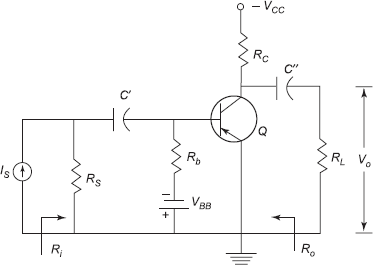
10.10 CURRENT SERIES FEEDBACK AMPLIFIER
The current series feedback amplifier is that amplifier where the current is sampled at the output of the amplifier and the output of β network is mixed with the input in series. In this configuration, the parameter stabilised is transconductance and the β of the feedback network is the ratio of the fedback voltage to the output voltage. The input impedance is enhanced by D, as in the voltage series amplifier, but the output impedance is also enhanced as required for a transconductance amplifier. The usual practice is performed for analysis of the circuit and the parameters are as follows:
|
D |
= |
1 + GMß |
|
GMf |
= |
GM/D |
|
Rif |
= |
RiD |
|
Rof |
= |
Ro(1 + G mβ) |
|
GM |
= |
GmRo/(Ro + RL) |
|
Rof′ |
= |
Ro′(1 + Gmβ)/D …(10.27) |
Figure 10.9 shows a common emitter circuit with emitter resistor in the emitter circuit. This is a very good example of current series feedback amplifier. The current in the emitter resistor Re develops a voltage, which is fed in series to the input source voltage. Thus, the output current (the base current being very small compared to collector current, emitter current can be assumed to be equal to the output collector current without loss in the reality) is sampled and is let through the feedback network, the emitter resistor and the voltage developed across it is fed back out of phase to the input source voltage. Thus, the circuit can be justified as current series feedback amplifier.
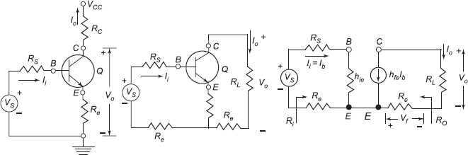
Fig. 10.9 Common emitter with Re
One more argument can be made assuming the drop across the collector and emitter being small, the reverse transmission factor being equal to feedback voltage to output voltage assuming the configuration to be voltage series. But, if so, β would be the ratio of Vf/Vo = − Re/RL, which violates the assumptions made with negative feedback amplifiers that the β is a function of load. Thus, this argument is ruled out and the configuration is current series.
The analysis can be carried in the usual manner and the following can be derived:
Feedback factor, β = − Re
Trans conductance, GM = − hfe/(Rs + hie + Re)
Desensitivity factor D = {Rs + hie + (1 + hfe)Re}/(Rs + hie + Re)
The parameter with feedback can this be determined to be
Trans conductance with feedback, |
GMf = − hfe/{Rs + hie + (1 + hfe) Re} |
Input impedance with feedback |
Rif = {Rs + hie + (1 + hfe)Re} |
Output impedance with feedback |
Rof = ∞ |
Effective output impedance |
Rof′ = Ro′ (1 + Gmβ)/D |
and |
Ro′ = Ro∥RL = RL …(10.28) |
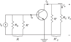
10.11 CURRENT SHUNT FEEDBACK AMPLIFIER
When current is sampled and the fedback signal is mixed in shunt with the input, the feedback amplifier is referred to as current shunt feedback amplifier. In this configuration, the stabilised parameter is current gain and the ratio of fedback current to output current is the transfer ratio of feedback circuit. The input impedance decreases and the output impedance increases and the analysis of the amplifier is as follows:
|
D |
= |
1 + AIβ |
|
AIf |
= |
AI/D |
|
Rif |
= |
Ri/D |
|
Rof |
= |
Ro(1 + Aiβ) |
|
AI |
= |
AiRo/(Ro + RL) |
|
Rof′ |
= |
Ro′(1 + Aiβ)/D …(10.29) |

Fig. 10.10 A current shunt feedback amplifier
An example of current shunt amplifier is as shown in Fig. 10.10, employing a two-stage transistor amplifier. The output current of the second stage is sampled and passed through the feedback resistor and mixed in shunt with the input current of the first stage. Thus, the circuit is an example of current shunt feedback amplifier. The analysis can be performed as usual.
Feedback factor |
β = Re/(R′ + Re) |
|
Current gain with feedback |
AIf = (R′ + Re)/Re |
|
Desensitivity factor |
D = 1 + AIβ |
…(10.30) |
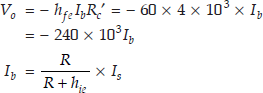
10.12 VOLTAGE SHUNT FEEDBACK AMPLIFIER
In a voltage shunt feedback amplifier, the output voltage is sampled and the feedback network output is mixed in shunt at the input of the amplifier. The parameter stabilised is transresistance and the β is the ratio of feedback current to output voltage. Thus, analysis follows and can be consolidated as
|
D = 1 + RMβ |
|
RMf = RM/D |
|
Rif = Ri/D |
|
Rof = Ro/(1 + βRm) |
|
RM = RMRL/(Ro + RL) |
|
Rof′ = Ro′/D …(10.31) |
Figure 10.11 shows a circuit that employs voltage shunt feedback. The output voltage is applied across the feedback resistor R′ (the output voltage is approximately equal to the collector to base voltage since the base to emitter voltage is very small and negligible compared to collector-base voltage) and the current resulting in this element is mixed in shunt with the input current. Thus, the feedback is voltage shunt and the analysis is as follows:

Fig. 10.11 Voltage-shunt feedback amplifier
β = − 1/R′ |
|
Mutual Resistance |
RM = − hfeRc′ R/(R + hie) |
where |
Rc′ = Rc∥R′ |
|
R = Rs∥R′ |
|
Ri = Rhie/(R + hie) …(10.32) |
SUMMARY
- Amplifiers can be classified based on the frequency of operation, coupling between stages, operating point selection or input and output parameters.
- Distortion in amplifier can be classified as amplitude, frequency or phase.
- A voltage amplifier is that amplifier where the input and output parameters of interest are voltage. It requires large input impedance and small output impedance.
- A current amplifier input is current and output is also current. Here, the input impedance should be very small and output very large.
- A transconductance amplifier has input as voltage and output as current. It requires both the impedances to be very high.
- A transresistance amplifier is that amplifier which has the input as current and output as voltage. It requires both impedances to be very low.
- Feedback in an amplifier is of two types: degenerative, where loop gain is less than unity, and regenerative, where the loop gain is greater than unity.
- Negative feedback in amplifiers is employed to stabilise some parameters and improve some other parameters of the amplifier. The only drawback with this is that the amplification is decreased.
- Four topologies possible with a negative feedback are voltage series, current series, current shunt and voltage shunt where voltage gain, transconductance, current gain and transresistance are stabilised, respectively.
- The input and output impedances of the amplifier are improved with negative feedback.
- Distortion is decreased, noise is decreased, stability is improved and bandwidth is increased by employing negative feedback in an amplifier.
10.1 An amplifier with open loop voltage gain of 1000 ± 20% is available. However, we desire to build an amplifier whose gain does not vary by more than 0.2%. Find the required feedback ratio β and the corresponding closed loop voltage gain.
Solution We have ![]()

Closed loop gain ![]()
10.2 If an input of 0.035 V peak to peak is given to an open loop amplifier, it gives fundamental frequency output of 45 Vpp but it is associated with 9% distortion (a) if the distortion is to be reduced to 1% how much feedback has to be introduced and what will be the required input voltage? (b) If 1.5% of V0 is feedback and the input maintained at the same level, what will be the output voltage?
Solution
- Let K′o2, K′o2 be the harmonic distortion without and with feedback, respectively.

We have Vo = 45 V, Vi = 0.035 V.
Open loop gain

From (1)
Since the gain is reduced by (1 + Aβ) times, that is, by 9 times, new value of Vi should be
Vi = 0.035 × 9 = 0.315 V -

New Vo = 0.035 × 63.38 = 2.218 V
10.3 An open loop amplifier has a midband gain of 500 and a pass band from 50 Hz to 50 kHz. Find voltage gain and cut off frequencies if 10% of output voltage is fed back.
Solution

10.4 An amplifier has an open loop voltage gain of 1000 and delivers 10 W output with 10% second-harmonic distortion when the input is 10 mV. Find the distortion if 60 dB of negative feedback is applied.
Solution We have, − 60 dB = − 20 log (1 + Aβ)

New value of second-harmonic distortion
10.5 An amplifier consists of three identical stages connected in series. The output voltage is sampled and returned to the input in series opposing. If it is specified that the relative change dAf/Af in the closed loop voltage gain Af must not exceed ψf, show that the minimum value of the open loop gain A of the amplifier is given by ![]() , where
, where ![]() is the relative change in the voltage gain of each stage of the amplifier.
is the relative change in the voltage gain of each stage of the amplifier.

Let A = overall gain of three stages


We have

Hence proved.
10.6
- An amplifier with voltage gain of 60 dB uses
 of its output in negative feedback. Calculate the gain with feedback in dB.
 - Voltage gain of an amplifier without feedback is 60 dB. It decreases to 40 dB with feedback. Calculate the feedback factor.
- A single-stage amplifier has a voltage gain of 600 without feedback, and 50 with feedback. Calculate the percentage of output which is feedback to the input.
- A = 60 dB = 20 log10 A ⇒ A = 103 = 1000

- Gain of the amplifier without feedback = 60 dB = A dB
⇒ A = 1000
Gain with feedback Af = 40 dB or 100.
We have

Feedback factor = βA = 9
- Gain without feedback = 600 = A
Gain with feedback = 50 = Af

% of output voltage feedback to input = β × 100
= 1.833%
10.7 A negative feedback of β = 0.002 is applied to an amplifier of gain 1000. Calculate the change in overall gain of the feedback amplifier if the internal amplifier is subjected to a gain reduction of 15%.
Solution Voltage gain without feedback A = 1000
Gain with feedback
When open loop gain is reduced by 15%
New voltage gain with feedback

Percentage change in overall gain

10.8 Prove that for voltage series feedback, with Rs = 0, Current gains with and without feed back are equal.
Solution For the voltage series feedback amplifier shown in the figure,

From the second mesh ![]()

Since ![]() ratio is independent of β. So we can say that AIf = AI.
ratio is independent of β. So we can say that AIf = AI.
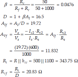
10.9 The transistors in the feedback amplifier are identical, and their h-parameters are same. Calculate ![]() A′Vf = Vo/Vi, AVf = Vo/Vs and Ro′f
A′Vf = Vo/Vi, AVf = Vo/Vs and Ro′f

Solution
β = 9.9 × 10⁻³ so this β is independent of Rs and RL. Here, voltage-series feedback is present.
To draw the circuit without feedback but taking loading of β into account
- To find input circuit. Set Vo = 0. Making output voltage shorted, we get 1000 Ω and 10 K in parallel at the emitter of first transistor.
- To find output circuit. Set Ii = 0 for series camparison we will have 1000 Ω and 10 K in series, at the collector of second transistor, by making B−E of transistor Q1 open.
Then, the circuit becomes as shown below:

Upon replacing transistor with their approximate h-parameter models,
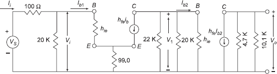
Gain of the amplifier without feedback = ![]()
Let AV1 ![]()
Here, second stage is CE amp.

![]() is obtained by using the formula for CE with Re.
is obtained by using the formula for CE with Re.

Since gain AV is desensitised here, AV1 f = AV1/D
∴ |
A′Vf = AV1/D = 93.04 |
|
Rif = Ri × D = 6.149 × 103 × 12.68 |
|
= 77.96 KΩ = 78 KΩ |
By using voltage division rule,

10.10 A voltage shunt feedback amplifier as shown in figure has a transistor with parameter hfe = 100, hie = 1 K. Assume approximate simplified model of the transistor. Assume Re = 0 to determine.


- Rif
- R′of
- Repeat the four preceding calculations with Re = 1 K.

Solution For Re = 0
Since the 100 K is common to both input node and output node, shunt connection exists.

Since this β is independent of Rs and RL, sampled signal should be voltage. So, the topology is voltage-shunt topology. We have to place a Norton’s source at the input.
To find 1nput circuit: Set Vo = 0. This short circuit at the output places 100 K from base to ground.
To find output circuit: Set Vi = 0, so 100 K is placed from collector to ground.
So, the circuit without feedback is as shown below:

Replacing transistor with its approximate model:

Since there is voltage-shunt feedback, it stabilises RM.


Ro = 100 K, RL = 10 K |
|
|
Vo = − hfe · Ib 100 K |

With Re = 1 KΩ. Here also voltage shunt connection exists. The diagram after replacing transistor with its equivalent is


where R′i = hie + (1 + hie)Re = 102.1 KΩ


10.11 Calculate ![]() Rif, Rof, R′of for the circuit shown below, use typical h-parameter values. Rs = RL = 10 K, Re = 1 KΩ.
Rif, Rof, R′of for the circuit shown below, use typical h-parameter values. Rs = RL = 10 K, Re = 1 KΩ.

Solution
- Identify the topology. Input loop is defined as loop containing B and E, output loop is the loop containing C and E. Since Re is common between input and output loops we can say that there exists a series mixing voltage across Re is the feedback signal Vf.
To find the signal sampled, assume first voltage is sampled.
 = 1. Since β is independent of Rs and Rc we can say that there is voltage sampling. So, the topology is voltage-series topology.
 - Draw the circuit without feedback.
- To find input circuit. Set Vo = 0 for voltage sampling, the circuit will be as shown below by looking into Base and Emitter terminals.

- To find output circuit, set Ii = 0 for series mixing. Then, Re and Rc will be series at the output terminals.

∴ the circuit without feedback will be as below:

- To find input circuit. Set Vo = 0 for voltage sampling, the circuit will be as shown below by looking into Base and Emitter terminals.
- Since Vf is feedback signal, Thevenin’s source is used.
- Replacing transistor with its proper model:

Since there is voltage series feedback, this stabilises voltage gain. Here, Rs has to be considered as part of the amplifier

Input resistance without feedback Ri = Rs + hie = 10 + 1.1 = 11.1 KΩ
For series mixing Rif = RiD = 11.1 × 5.5 × 103
= 61.05 KΩ
We are interested in output resistance seen looking into the emitter Ro′ = Re = 1 KΩ

10.12 For the FET circuit, using feedback analysis techniques find AVf, Rif, Rof, R′of if Rs = 10 KΩ , gm = 10 mA/V, rd = 1 MΩ.
Solution
- Since Rs is common between G-S and D-S loops, we confirm that there is a series mixing. Assuming sampled signal as voltage
 Therefore, there is a voltage series topology in the circuit.

- To find input circuit, set Vo = 0. To find output circuit, open circuit the input terminals. The circuit without feedback but taking loading of β network into account will be

- Replacing FET with its low-frequency model,

This topology stabilises voltage gain.

Since there is an open circuit, between gate and source, Ri = ∞
∴ Rif = ∞
From the circuit Ro = rd, β = 1


10.13 For the two-stage amplifier circuit shown in figure, Assume Rs = 0, hfe = 50, hie = 1100 Ω, hre = hoe = 0 and indentical transistors. Find AVf, Rif, Rof.
Solution
- Input is applied at the base of first transistor and output is taken from the collector of second transistor. Since the feedback network consisting of the potential divider arrangement of R1 and R2, voltage across R1 is fed back to the input. So, there exists a series mixing, and voltage across R1 is the feedback signal.

∴
 using voltage division.
 since this β is independent of Rs and RL, we can confirm there is voltage sampling so, voltage series feedback is present.
 - To find input circuit, set Vo = 0. then R1 and R2 will be in parallel, at the emitter of transistor Q1. To find output circuit set Ii = 0, then series connection of R1 and R2 will be at the collector of transistor Q2. The circuit without feedback but taking loading of β network into account will be as shown.
This topology stabilises voltage gain. AV = AV1 · AV2 where AV1 and AV2 are the voltage gains of first and second stages, respectively. First stage is CE with Re and second stage is CE. On replacing transistors with their h-parameter models.

Effective load resistance of Q1, RL1 = 22 K||220 K||22 K||hie
= 22 K||20||1.1 K
= 1.002 KΩ
Effective load resistance of Q2 is RL2 = 22 K||1500
= 1.404 KΩ

Total input resistance is decided by the input resistance of the first stage.
Ri = hie + (1 + hfe)Re
= 1.1 K + 51 × 333.33 =18.09 KΩ
Rif = Ri · D = 1083.22 KΩ
Total output resistance is decided by the output resistance of second stage.


10.14 In a CE amplifier with unbypassed Re, Rs = 0, RL = 4 K, Re = 1 K, find AVf, Rif, use typical h-parameter values.
Solution
- Re is common between input loop and output loop. So, there is series mixing present, voltage across Re is the feedback signal. Assume sampled signal is Vo,


Here, β is dependent upon RL, so voltage sampling is not possible. So current is the sampled signal. Here, the topology is current-series feedback which stabilises GM.
- To find input circuit, set Io = 0. Then Re is connected between emitter and signal source. To find output circuit, set Ii = 0. Then, Rc and Re will be in series, at the collector voltage across Re is the feedback signal Vf.

- Replacing transistor with its approximate h -parameter model,


= − 0.96 × 10−3 × 4 × 103 = − 3.84.
Ri = Rs + hie + Re = 0 + 1.1 K + 1 K = 2.1 KΩ
Rif = Ri × D = 2.1 × 24.80 × 103 = 52.08 KΩ
10.15 The circuit has following parameters Rc1 = 2.5 KΩ, Rc2 = 600 Ω, Re = 50 Ω, Rf = Rs = 1 KΩ, hfe = 50, hie = 1.1 KΩ, hre = hoe = 0. Find (a) AVf (b) Rif (c) The output resistance.
Solution
- Since Io current is following through emitter resistance Re, and Rf is connected to the base node, there exists a shunt connection. To find the signal that is sampled, write an expression for feedback current.


∴
 is independent of Rs and RL, so sampled signal is current.
There is current-shunt topology present.
- To find input circuit, set Io = 0 for current sampling. Then, Rf and Re will be in series and appear at the base of transistor Q1. To find output circuit, set Vi = 0 , for shunt comparison. Then, Rf and Re will be in parallel, at the emitter of Q2. Since there is shunt mixing, we have to use Norton’s source at the input.
- Replacing transistor’s with their proper model,

This topology stabilises current gain

From the circuit,
 = − hfe = − 50
Ri2 = hie + (1 + hfe) (Re∥Rf) (Since second stage is CE with Re)
= 1.1 + (51) (50 ∥1000)
= 3528.5 Ω
Since R = Rs∥Rf = 1 K ∥1 K = 500
∴
AI = (− 50) (− 0.4167) (50) (0.3125)
= 325.54
If Rc2 is an external load, then Ro = ∞, Rof = ∞


10.16 The circuit has following parameters Rc = 4 K, R′ = 50 K, Rs = 6 KΩ, hie = 1.1 KΩ, hfe = 60 and hoe = hre = 0. Find (a) AVf (b) Rif and (c) Rof.

- Since R′ is common between input node (base) and output node (c), there exists a shunt connection. The feedback signal is current If.
To find the way of sampling,

Since Vo ≫ Vi,
 Since β = − 1/R′ is independent of load Rc and Rs, there is voltage sampling. This is a voltage-shunt topology. This stabilises “Transresistance” (RM).
 - To find input circuit, set Vo = 0. Then, R′ appears between base and ground. To find the output circuit, set Vi = 0 for shunt comparison. Then R′ appears between collector and ground.
The circuit will be,
Here current source has been used since there is shunt mixing.
Let
R′c = Rc∥R′ = 4 K∥50 K = 3.70 KΩ
R = Rs∥R′ = 6 K∥50 K = 5.35 KΩ
Replacing transistor with its proper model,


If Rc is considered as load, Ro = R′ = 50 KΩ


10.17 Determine the input impedence of all types of feedback amplifiers.
Solution Voltage series feedback:

From the input circuit, we have
Using voltage division in the output circuit
where ![]()
|
Vs = IiRi + βAVIiRi |
|
= RiIi (1 + βAV) |
∴ |
|
Av = open circuit voltage gain without feedback, and AV = voltage gain without feedback taking RL into account. Therefore,
Current series feedback:
Writing KVL in the input circuit,
Using current division, Io from output circuit is given by
where ![]()
|
Vs = IiRi + βGMVi |
|
= IiRi + βGMIiRi |
|
= IiRi (1 + βGM) |
![]() When there is series mixing input resistance increases with feedback Gm is short-circuit transconductance. GM is the trans-conductance without feedback taking load into account.
When there is series mixing input resistance increases with feedback Gm is short-circuit transconductance. GM is the trans-conductance without feedback taking load into account.
Current-shunt feedback:

Writing KCL at the input node,
Using current division, at the output circuit
where ![]()
Is = Ii + βAI·Ii |
|
|
= Ii(1 + βAI) |
We have ![]()
∴ ![]() so we can say that with shunt mixing Rif < Ri
so we can say that with shunt mixing Rif < Ri
where Ai is the short circuit current gain taking Rs into account, AI is current gain without feedback taking RL into account.
Voltage-shunt feedback:

Writing KCL at the input node,
From voltage division,
where ![]()
∴ Is = Ii(1 + βRM)
We know that ![]()

Rm is the transresistance under open-circuit. RM is the transistance without feedback but taking the load into account.
Therefore, when there is shunt mixing Rif < Ri
10.18 Determine the output impedance of all types of feedback amplifiers.
Solution Voltage series feedback:
Put an arbitrary voltage source of value V and assume it is sending a current I, by making RL = ∞, and VS = 0 then the circuit becomes,
Then, ![]()
From the output circuit
(∴ with Vs = 0, Vf + Vi = 0 ∴ Vi = − Vf = − βV)

and, ![]()
![]() so we can say that with voltage sampling Rof < Ro
so we can say that with voltage sampling Rof < Ro
Current series feedback:
By making Vs = 0, RL = ∞, and introducing a voltage source of value V, assuming that it is sending a current 1 into the circuit, the circuit becomes,

From the output circuit
Writing KVL in the input loop,

Therefore, for current sampling Rof > Ro
R′of = output resistance with feedback taking RL into account
Since ![]()
Current-shunt feedback:
The circuit with Is = 0, and RL = ∞ will be

From the input circuit, writing KCL
|
Ii + If = 0 |
|
Ii + βIo = 0 ⇒ Ii = βI …(1) |
From the output circuit,


where R′o = Ro ∥ RL
![]() Therefore, for current sampling Rof > Ro.
Therefore, for current sampling Rof > Ro.
Voltage-Shunt Feedback:
By making Is = 0, and impressing a voltage source of value V by making RL = ∞.
The circuit becomes

Writing KCL at input node
|
Ii + βV = 0 |
∴ |
Ii = − βV …(1) |
From the output circuit,

Since ![]()
We have ![]()
∴ for voltage sampling Rof < Ro.
EXERCISE PROBLEMS
10.1 For the circuit shown, with Rc = 4 k = RL, Rb = 20 k, Rs = 1 K and with typical h -parameter values. Find
- AI = IL/Is


- The input resistance seen by the source.
- The output resistance seen by the load.
10.2 Repeat the above problem, with gm = 5 mA/V, rd = 100 K.

10.3 We have an amplifier of gain 100 dB. It has an output impedance Zo = 100 KΩ. It is required to modify its output impedance to 500 Ω by applying negative feedback. Calculate the value of β. Calculate the percentage change in the overall gain.
10.4 For the transistor amplifier hfe = 100, hie = 1 K and hre = hoe = 0. Find with Re = 0.


- Rif and
- Rof
- Repeat with Re = 500 Ω

10.5 For the FET amplifier shown below has gm = 50 mA/V, rd = 1 MΩ. Find Avf, Rif, Rof, with Rs = 2 KΩ.

10.6 Find Avf, Rif, Rof for the circuit shown below. If Rs = 0, hfe = 50, hie = 1100 Ω, hoe = 0. Assume Identical transistors.

10.7 Find Avf, GMf, Rif, Rof, R′of for the circuit shown below. hfe = 150, hie = 1000 Ω, hre = hoe = 0 and Rs = 1 KΩ.

10.8 For the following circuit, Rc1 = 3 K, Rc = 3 K, Re = 50 Ω, R′ = Rs = 1000 Ω, hfe = 50, hie = 1.1 K and hre = hoe = 0. Find (a) Avf (b) Rif (c) Rof.

Review Questions
- Classify amplifiers based on frequency, operating point, coupling between stages and input and output parameters. Discuss.
- Discuss in detail the types of distortion in an amplifier.
- What is feedback? Why is it employed in an amplifier circuit? How many types of feedback are possible? Discuss.
- What is negative feedback? Discuss how it can improve stability in an amplifier.
- Enumerate the advantages and disadvantages with negative feedback in an amplifier.
- Derive an expression for the transfer gain of a feedback amplifier.
- What are the various types of amplifiers based on the output and input parameters? Give their equivalent circuits and ideal characteristics.
- Discuss in detail about the types of negative feedback amplifiers giving the effect of each type of feedback on the parameters of the amplifier.
- Derive an expression for the input impedance with feedback of a voltage shunt feedback amplifier.
- Derive an expression for the input impedance and output impedance with feedback of a voltage series feedback amplifier.
- Derive an expression for the output impedance with feedback of a current shunt feedback amplifier.
- Derive an expression for the input and output impedance with feedback of a current series feedback amplifier.
- Enumerate the procedure employed in the analysis of a feedback amplifier and discuss in detail the effect of feedback on the amplifier parameters.
- Discuss how to separate basic amplifier circuit and the feedback circuit from a feedback amplifier circuit.
- Derive an expression for the input impedance with feedback of a feedback amplifier, which stabilises current gain.
- Define the following modes of operation of an amplifier: class A, class B, class AB and class C. Compare them based on the efficiency and distortion.
- Draw a feedback amplifier in block diagram form and explain each block in detail giving its functions.
- What are the four topologies of a feedback amplifier? Identify all the signals and transfer gains of each topology.
- Distinguish between regenerative and degenerative feedback in amplifiers and give their applications.
- Define desensitivity factor D. Give its significance in negative feedback amplifiers.
- Draw a voltage series feedback amplifier employing FET and analyse it.
- What are assumptions made in the negative feedback amplifiers?
- What sort of feedback is employed in a CE amplifier with unbypassed emitter resistor? Discuss its analysis in detail.
- Draw the circuit diagram of a voltage shunt feedback amplifier and explain the feedback and give the expression for D.
- Classify amplifiers based on the coupling between two stages.