
![]()
MCP23017 GPIO Extender
Microchip’s MCP23017 provides 16 additional GPIO pins that can be purchased for as little as $1.99. The chip communicates using the I2C bus. (The companion MCP23S17 is available for SPI bus.) The I2C bus allows the chip to be remote from the Raspberry Pi, requiring only a four-wire ribbon cable (power, ground, and a pair of I2C bus lines). This chapter explores the features and limits of this peripheral.
DC Characteristics
When shopping for chips or interface PCBs based on a particular chip, the first thing I look at is the operating supply voltage. 5 V parts are inconvenient for the Pi because of its 3.3 V GPIO interface. Many newer devices operate over a range of voltages, which include 3.3 V. The MCP23017 supply VDD operates from an extended range of +1.8 V to +5.5 V. This clearly makes it compatible, if we power the chip from a +3.3 V source. Figure 2-1 shows the MCP23017 chip pinout diagram.
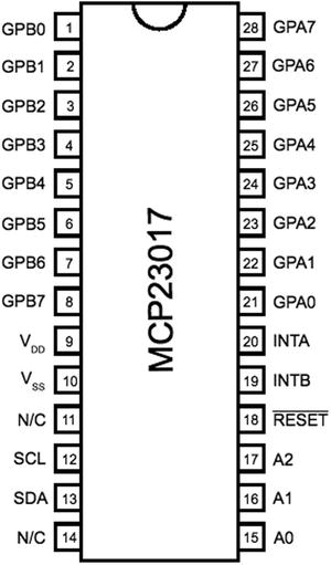
Figure 2-1. MCP23017 pinout
Another factor in choosing a peripheral chip is its output drive capability. How well can the GPIO pin source or sink current? As covered in Chapter 10 of Raspberry Pi Hardware Reference (Apress, 2014), the Raspberry Pi’s own GPIO pins can source/sink up to 16 mA, depending on configuration. The MCP23017 chip specifications indicate that it can source or sink up to 25 mA.
We still need to remember that if the MCP23017 is powered from the Raspberry Pi’s 3.3 V regulator on header P1, the total current budget must not exceed 50 mA. This budget includes the Pi’s own GPIO pin current usage. If, on the other hand, the MCP23017 is powered from a separate 3.3 V power supply, this limitation is eliminated.
There are still reasons to budget current, however. The chip must not consume more than 700 mW of power. This implies a total current limit as follows:

This power figure gives us an upper current limit. However, the datasheet of the MCP23017 also lists a maximum of 125 mA for supply pin VDD. If every GPIO output is sourcing power, this leaves us with the following average pin limit:
![]()
So while the output GPIO pins can source up to 25 mA, we cannot have all of them doing so simultaneously.
Likewise, the datasheet lists VSS (ground) as limited to an absolute maximum of 150 mA. If every GPIO pin is an output and sinking current, the average for each output pin cannot exceed the following:
![]()
Once again, while each output pin can sink up to 25 mA, we see that they cannot all do so at the same time without exceeding chip limits. This should not be discouraging, because in most applications, not all GPIO pins will be outputs, and not all will all be driving heavy loads. The occasional pin that needs driving help can use a transistor driver like the one discussed in Chapter 10 of Raspberry Pi Hardware Reference (Apress, 2014).
Before we leave the topic of GPIO output driving, we can apply one more simple formula to help with interface design. With the foregoing information, we can calculate the number of 25 mA outputs available:
![]()
From this, it is known that four to five GPIO pins can operate near their maximum limits, as long as the remaining GPIO pins are inputs or remain unconnected.
In normal operation, the GPIO inputs should never see a voltage below the ground potential VSS. Nor should they ever see a voltage above the supply voltage VDD. Yet, variations can sometimes happen when interfacing with the external world, particularly with inductive components.
The datasheet indicates that clamping diodes provide some measure of protection against this. Should the voltage on an input drop below 0, it is clamped by a diode so it will not go further negative and cause harm. The voltage limit is listed at –0.6 V, which is the voltage drop of the clamping diode. Likewise, if the voltage goes over VDD (+3.3 V in our case), the clamping diode will limit the excursion to VDD + 0.6 V (+3.9 V).
This protection is limited by the current capability of the clamping diodes. The datasheet lists the maximum clamping current as 20 mA. If pins are forced beyond their limits and the clamping current is exceeded, damage will occur.
While we have focused on GPIO inputs in this section, the clamping diodes also apply to outputs. Outputs can be forced beyond their limits by external circuits like pull-up resistors. Pull-up resistors should not be attached to +5 V, for example, when the MCP23017 is operating from a +3.3 V supply.
If the MCP23017 device is not sourcing or sinking output currents, the standby current is stated as 3 μ A (for 4.5 to 5.5 V operation). This operating parameter is important to designers of battery-operated equipment.
Since the device operates over a range of supply voltages, the datasheet defines the logic levels in terms of the supply voltage. For example, the GPIO input low level is listed as 0.2 × VDD. So if we operate with VDD= +3.3 V, the input low voltage is calculated as follows:

Therefore, a voltage in the range of 0 to 0.66 V is guaranteed to read as a 0 bit.
Likewise, let’s calculate the input high voltage threshold, where the multiplier is given as 0.8:
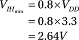
Thus any voltage greater than or equal to 2.64 V is read as a 1 bit, when powered from a +3.3 V supply. Any voltage between VILmax and VIHmin is undefined and reads as a 1 or a 0, and perhaps randomly so.
Output Logic Levels
The output logic levels are stated differently. The datasheet simply states that the output low voltage should not exceed a fixed limit. The high level is also stated as a minimum value relative to VDD. This pair of parameters is listed here:

The only parameter of interest for timing apart from the I2C bus is the device reset time. In order for the device to see a reset request, pin ![]() must remain active (low) for a minimum of 1 μs. The device resets and places outputs into the high-impedance mode within a maximum of 1 μs.
must remain active (low) for a minimum of 1 μs. The device resets and places outputs into the high-impedance mode within a maximum of 1 μs.
Circuit
Figure 2-2 shows a circuit with two remote MCP23017 GPIO extenders connected to one I2C bus. In the figure, the power, ground, I2C data, and optional ![]() and
and ![]() connections are shown connected through a six-conductor ribbon cable. This allows the Raspberry Pi to communicate remotely to peripherals in a robot, for example.
connections are shown connected through a six-conductor ribbon cable. This allows the Raspberry Pi to communicate remotely to peripherals in a robot, for example.
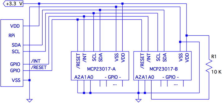
Figure 2-2. MCP23017 circuit
The data communication occurs over the pair of signals SDA and SCL. These are connected to the Raspberry Pi’s pins P1-03 and P1-05, respectively (GPIO 2 and 3 for Rev 2.0+). The other end of the I2C data bus is common to all slave peripherals.
Each MCP23017 slave device is addressed by its individually configured A2, A1, and A0 pins. For device A, these pins are shown grounded to define it as device number 0x20 (low bits are zeroed). A1 is tied high for device B so that its peripheral address becomes 0x21. In this configuration, the Raspberry Pi will use addresses 0x20 and 0x21 to communicate with these slave devices.
Lines labeled ![]() and
and ![]() are optional connections. The
are optional connections. The ![]() line can be eliminated if you never plan to force a hardware reset of the slaves (tie to VDD through a 10 K resistor). Usually the power-on reset is sufficient. The
line can be eliminated if you never plan to force a hardware reset of the slaves (tie to VDD through a 10 K resistor). Usually the power-on reset is sufficient. The ![]() line is more desirable, since the MCP23017 can be programmed to indicate interrupts when a GPIO input has changed in value (or does not match a comparison value). The
line is more desirable, since the MCP23017 can be programmed to indicate interrupts when a GPIO input has changed in value (or does not match a comparison value). The ![]() line is an open collector pin so that many can be tied together on the same line. However, the Pi will have to poll each peripheral to determine which device is causing the interrupt. Alternatively, each slave could provide a separate
line is an open collector pin so that many can be tied together on the same line. However, the Pi will have to poll each peripheral to determine which device is causing the interrupt. Alternatively, each slave could provide a separate ![]() signal, with a corresponding increase in signal lines.
signal, with a corresponding increase in signal lines.
Each MCP23017 chip has two interrupt lines, named ![]() and
and ![]() . There is the option of separate interrupt notifications for the A group or the B group of GPIO pins. For remote operation, it is desirable to take advantage of MCP23017’s ability to configure these to work in tandem, so that only one
. There is the option of separate interrupt notifications for the A group or the B group of GPIO pins. For remote operation, it is desirable to take advantage of MCP23017’s ability to configure these to work in tandem, so that only one ![]() line is required.
line is required.
On the Raspberry Pi end, the GPIO pin used for the ![]() line would be configured as an output and held high, until a reset is required. When activating a reset, the line must be held low for at least 1 microsecond, plus 1 more microsecond to allow for the chip reset operation itself (and possibly longer, if non-MCP23017 slaves are connected to the bus).
line would be configured as an output and held high, until a reset is required. When activating a reset, the line must be held low for at least 1 microsecond, plus 1 more microsecond to allow for the chip reset operation itself (and possibly longer, if non-MCP23017 slaves are connected to the bus).
The ![]() line should be connected to a GPIO input on the Pi. This GPIO input either needs to be polled by the application, or to have the GPIO configured to trigger on changes. Then the select(2) or poll(2) system calls can be used to detect when an interrupt is raised by one or more peripherals.
line should be connected to a GPIO input on the Pi. This GPIO input either needs to be polled by the application, or to have the GPIO configured to trigger on changes. Then the select(2) or poll(2) system calls can be used to detect when an interrupt is raised by one or more peripherals.
The interrupt line, when used, should have a pull-up resistor configured (see Chapter 10 of Raspberry Pi Hardware Reference [Apress, 2014] for information about internal pull-up resistors). It may be best to use an external pull-up resistor, especially for longer cable runs. To keep the sink current at 2 mA or less, the pull-up resistance used should be no lower than the following:
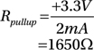
A 2.2 kΩ 10% resistor will do nicely.
The +3.3 V line should be powered separately from the Raspberry Pi, unless the slaves expect to drive very low currents. The main concern here is to not overload the remaining 50 mA capacity of the Pi’s +3.3 V regulated supply. See Chapter 10 of Raspberry Pi Hardware Reference (Apress, 2014) about budgeting +3.3 V power.
I2C Bus
Throughout this chapter, we are assuming a Rev 2.0 or later Raspberry Pi. This matters for the I2C bus because the early versions wired I2C bus 0 to P1-03 and P1-05 (GPIO 0 and 1). Later this was changed to use bus 1. See Chapter 12 of Raspberry Pi Hardware Reference (Apress, 2014) for more information about identifying your Pi and which I2C bus to use. If you are using an early Raspberry Pi revision, you’ll need to substitute 0 for bus number 1, in commands and in the C source code that follows.
Wiring and Testing
The connections to the MCP23017 are simple enough that you can wire it up on a breadboard. The first step after wiring is to determine that you can detect the peripheral on the I2C bus.
But even before that, check your kernel module support. If lsmod doesn’t show these modules loaded, you can manually load them now:
$ sudo modprobe i2c−dev
$ sudo modprobe i2c−bcm2708
If you haven’t already done so, install i2c-tools:
$ sudo apt−get install i2c−tools
If your I2C support is there, you should be able to list the available I2C buses:
$ i2cdetect −l
i2c −0  unknown        bcm2708_i2c.0                  N/A
i2c −1  unknown        bcm2708_i2c.1                  N/A
The I2C device nodes should also appear in /dev. These nodes give us access to the I2C drivers:
$ ls −l /dev/i2c∗
crw−rw−−−T  1  root root  89, 0  Feb 18 23:53  /dev/i2c−0
crw−rw−−−T  1  root root  89, 1  Feb 18 23:53  /dev/i2c−1
The ultimate test is to see whether the MCP23017 chip is detected (change the 1 to 0 for older Pi revisions):
$ sudo i2cdetect −y 1
     0  1  2  3  4  5  6  7  8  9  a  b  c  d  e  f
00:          −− −− −− −− −− −− −− −− −− −− −− −− −−
10: −− −− −− −− −− −− −− −− −− −− −− −− −− −− −− −−
20: 20 −− −− −− −− −− −− −− −− −− −− −− −− −− −− −−
30: −− −− −− −− −− −− −− −− −− −− −− −− −− −− −− −−
40: −− −− −− −− −− −− −− −− −− −− −− −− −− −− −− −−
50: −− −− −− −− −− −− −− −− −− −− −− −− −− −− −− −−
60: −− −− −− −− −− −− −− −− −− −− −− −− −− −− −− −−
70: −− −− −− −− −− −− −− −−
In this example, the A2, A1, and A0 pins of the MCP23017 were grounded. This gives the peripheral the I2C address of 0x20. In the session output, we see that address 0x20 was detected successfully.
The i2cdump utility can be used to check the MCP23017 register:
$  sudo  i2cdump  –y  –r   0x00–0x15 1 0x20 b
     0  1  2  3  4  5  6  7  8  9  a  b  c  d  e  f  0123456789abcdef
00: ff ff 00 00 00 00 00 00 00 00 00 00 00 00 00 00  ................
10: 00 00 00 00 00 00                                ......
Here we have dumped out registers 0x00 to 0x15 on I2C bus 1, at peripheral address 0x20, in byte mode. This was performed after a power-on reset, so we can check whether the register values match the datasheet values documented. As expected, IODIRA (register 0x00) and IODIRB (register 0x01) have the default of all 1s (0xFF). This also confirms that the registers are in BANK=0 mode (this is discussed in the following sections). All other MCP23017 registers default to 0 bits, which is also confirmed.
The MCP23017 datasheet describes the full register complement and options available. In this chapter, we’ll concern ourselves with a subset of its functionality, which is perhaps considered “normal use.” The extended functionality is left as an exercise for you.
For this chapter’s project, we’re going to do the following:
- Configure some GPIOs as inputs
- Configure some GPIOs as outputs
- Configure the group A and B inputs to signal an interrupt on any change
General Configuration
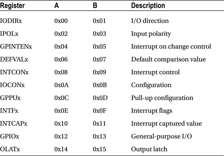
The MCP23017 peripheral has 10 registers for the GPIO-A pins, 10 registers for the GPIO-B pins, and one shared register. In other words, there are 22 registers, with one pair of addresses referencing a common register. These registers may be accessed in banks or interleaved. We’ll use interleaved mode in this chapter, to avoid having to reset the device.
Interleaved register addresses are shown in Table 2-1. These are valid addresses when the IOCON register value for BANK=0 (discussed later in this section).
Table 2-1. MCP23017 Register Addresses
This is the first register that must be configured, since it affects how registers are addressed. Additionally, other settings are established that affect the entire peripheral.
Table 2-2 illustrates the layout of the IOCON register. Setting the BANK bit determines whether we use banked or interleaved register addressing. The MCP23017 is in interleaved mode after a power-on reset. Once you set BANK=1, the register addresses change. However, once this change is made, it is impossible to tell, after a program restart, which register mode the peripheral is in. The only option is a hardware reset of the MCP23017 chip, to put it in a known state. For this reason, we’ll keep the peripheral in its power-on reset state of BANK=0.
Table 2-2. IOCON Register
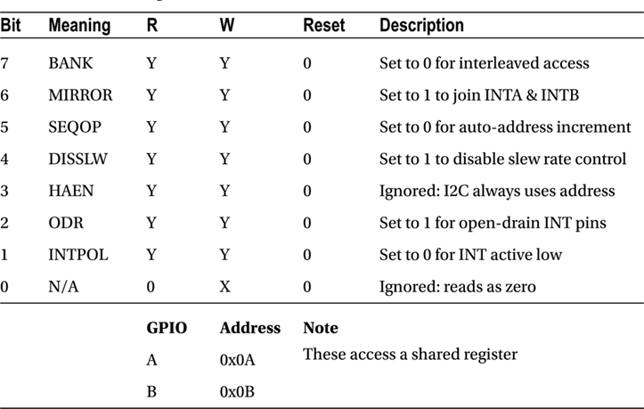
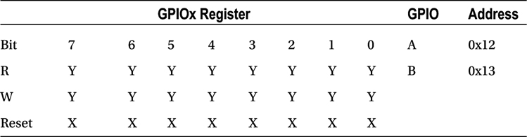
In the tables that follow, a Y under the R (read) or W (write) column/row indicates that you can read or write the respective value. The Reset column indicates the state of the bit after a device reset. An X indicates a “don’t care” or an undefined value when read. An N indicates no access or no effect when written.
The bit MIRROR=1 is used to make ![]() equivalent to
equivalent to ![]() . In other words, GPIO A and B interrupts are reported to both pins. This allows a single pin to be used for A and B groups.
. In other words, GPIO A and B interrupts are reported to both pins. This allows a single pin to be used for A and B groups.
Setting bit SEQOP=0 allows the peripheral to automatically increment the register address as each byte is read or written. This eliminates the need to transmit a register address in many cases.
Bit DISSLW affects the physical handling of the SDA I2C bus line.
HAEN is applicable only to the MCP23S17 SPI device, since addresses are always enabled for I2C devices.
This project uses ODR=1 to configure the ![]() pin as an open-drain pin. This allows multiple MCP23017 devices to share the same interrupt line. Use a pull-up resistor on the
pin as an open-drain pin. This allows multiple MCP23017 devices to share the same interrupt line. Use a pull-up resistor on the ![]() line when this is in effect. Otherwise, you may experience several sporadic interrupts.
line when this is in effect. Otherwise, you may experience several sporadic interrupts.
Finally, INTPOL=0 is configured so that the interrupt is active low. This is required for an open-drain connected line along with a pull-up resistor.
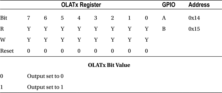
GPIO pins are all configured as inputs after a power-on reset (or use of ![]() ). Prior to configuring pins as outputs, it is usually a good idea to set the required output values. This is accomplished by writing the OLAT register, for group A or B. For this project, we’ll just write 0x00 to both OLATA and OLATB.
). Prior to configuring pins as outputs, it is usually a good idea to set the required output values. This is accomplished by writing the OLAT register, for group A or B. For this project, we’ll just write 0x00 to both OLATA and OLATB.
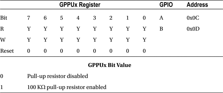
A given project should also define a known value for its input pull-up resistors. Setting a given bit to 1 enables a weak 100 KΩ internal pull-up resistor. This setting affects only the inputs. The pull-up resistors are configured off after a reset. In our example code, we turn them on.
This register is associated with interrupt processing. Interrupts are produced from conditions arising from input GPIO pins only. An interrupt can be generated if the input differs from the DEFVALx register or if the input value has changed. In the project presented, we simply zero this value because it is not used when detecting changed inputs.

This register specifies how input comparisons will be made. In our project, we set all these bits to 0 so that inputs interrupt on change.
Bits set in this register will invert the logic sense of the corresponding GPIO inputs. In our project, we used no inversion and set the bits to 0.

This register determines whether a given GPIO pin is an input or an output. Our project defines bits 4 through 7 as inputs, with the remaining bits 0 through 3 of each 8-bit port as outputs.

This register enables interrupts on input pin events. Only inputs generate interrupts, so any enable bits for output pins are ignored. How the interrupt is generated by the input is determined by registers DEFVALx and INTCONx.
For this project, we enabled interrupts on all inputs for ports A and B.
This interrupt flags register contains the indicators for each input pin causing an interrupt. This register is unwritable.
Interrupt service routines start with this register to identify which inputs are the cause of the interrupt. The DEFVALx and INTCONx registers configure how those interrupts are generated. The INTFx flags are cleared by reading the corresponding INTCAPx or GPIOx register.
The interrupt capture register reports the status of the inputs as the interrupt is being raised. This register is read-only. Reading this register clears the INTFx register, to allow new interrupts to be generated. When ![]() is linked to
is linked to ![]() , both INTCAPA and INTCAPB must be read to clear the interrupt (or read the GPIOx registers).
, both INTCAPA and INTCAPB must be read to clear the interrupt (or read the GPIOx registers).
Reading this register provides the current input pin values, for pins configured as inputs. Reading the GPIOx register also clears the interrupt flags in INTFx. When ![]() is linked to
is linked to ![]() , both GPIOA and GPIOB must be read to clear the interrupt (or read the INTCAPx registers).
, both GPIOA and GPIOB must be read to clear the interrupt (or read the INTCAPx registers).
Presumably, the OLATx register is read, for pins configured for output (the datasheet doesn’t say). Writing to the GPIOx register alters the OLATx settings in addition to immediately affecting the outputs.

Main Program
Here are some change notes for the main program:
- If you have a pre-revision 2.0 Raspberry Pi, change line 36 to use /dev/i2c-0.
- Change line 55 if your MCP23017 chip is using a different I2C address than 0x20 (A2, A1, and A0 grounded).
- Change line 56 if you use a different Raspberry Pi GPIO for your interrupt sense pin.
The main program is fairly straightforward. Here are the basic overall steps:
- A signal handler is registered in line 180, so ^C will cause the program to exit cleanly.
- Routine i2c_init() is called to open the I2C driver and initialize.
- Routine mcp23017_init() is called to initialize and configure the MCP23017 device on the bus (only one is currently supported).
- Routine gpio_open_edge() is called to open /sys/class/gpio17/value, so changes on the interrupt line can be sensed. This is discussed in more detail later.
- Finally, the main program enters a loop in lines 190 to 200, looping until ^C is entered.
Once inside the main loop, the following events occur:
- Execution stalls when gpio_poll() is called. This blocks until the interrupt on GPIO 17 transitions from a high to a low.
- The interrupt flags are read using routine mcp23017_interrupts(). They’re only reported and otherwise not used.
- Routine mcp23017_captured() is used to read the INTCAPA and INTCAPB registers in order to clear the interrupt.
- Finally, the routine post_outputs() reads the real-time input values and sends the bits to the outputs.
Program mcp23017.c is shown here:
1    /∗∗∗∗∗∗∗∗∗∗∗∗∗∗∗∗∗∗∗∗∗∗∗∗∗∗∗∗∗∗∗∗∗∗∗∗∗∗∗∗∗∗∗∗∗∗∗∗∗∗∗∗∗∗∗∗∗∗∗∗∗∗∗∗∗∗∗∗∗
2    ∗ mcp23017.c :  Interface with MCP23017 I/O Extender Chip
3    ∗
4    ∗ This code assumes the following :
5    ∗
6    ∗      1.   MCP23017 is configured for address 0x20
7    ∗      2.   RPi's GPIO 17 (GEN0) will be used for sensing interrupts
8    ∗      3.   Assumed there is a pull up on GPIO 17.
9    ∗      4.   MCP23017 GPA4-7 and GPB4–7 will be inputs, with pull-ups.
10   ∗      5.   MCP23017 GPA0–3 and GPB0–3 will be ouputs.
11   ∗      6.   MCP23017 signals interrupt active low.
12   ∗      7.   MCP23017 operating in non–banked register mode.
13   ∗
14   ∗  Inputs sensed will be copied to outputs :
15   ∗      1. GPA4–7 copied to GPA0–3
16   ∗      2. GPB4–7 copied to GPB0–3
17   ∗
18   ∗∗∗∗∗∗∗∗∗∗∗∗∗∗∗∗∗∗∗∗∗∗∗∗∗∗∗∗∗∗∗∗∗∗∗∗∗∗∗∗∗∗∗∗∗∗∗∗∗∗∗∗∗∗∗∗∗∗∗∗∗∗∗∗∗∗∗∗/
19
20  #include <stdio.h>
21  #include <stdlib.h>
22  #include <fcntl.h>
23  #include <unistd.h>
24  #include <string.h>
25  #include <errno.h>
26  #include <signal.h>
27  #include <assert.h>
28  #include <sys/ioctl.h>
29  #include <sys/poll.h>
30  #include <linux/i2c.h>
31  #include <linux/i2c–dev.h>
32
33  #include "i2c_funcs.c"              /∗ I2C  routines  ∗/
34
35  /∗ Change to i2c 0 if using early Raspberry Pi ∗/
36  static const char ∗ node = "/dev/i2c–1";
37
38  #define GPIOA        0
39  #define GPIOB        1
40
41  #define IODIR        0
42  #define IPOL         1
43  #define GPINTEN      2
44  #define DEFVAL       3
45  #define INTCON       4
46  #define IOCON        5
47  #define GPPU         6
48  #define INTF         7
49  #define INTCAP       8
50  #define GPIO         9
51  #define OLAT         10
52
53  #define MCP_REGISTER(r,g) (((r) <<1)|(g)) /∗ For I2C routines ∗/
54
55  static unsigned gpio_addr = 0x20;   /∗ MCP23017 I2C Address ∗/
56  static const int gpio_inta = 17;    /∗ GPIO pin for INTA connection ∗/
57  static int is_signaled = 0;         /∗ Exit program if signaled ∗/
58
59  #include "sysgpio.c"
60
61  /∗
62   ∗ Signal handler to quit the program  :
63   ∗/
64  static void
65  sigint_handler(int signo) {
66          is_signaled = 1;            /∗ Signal to exit program ∗/
67  }
68
69  /∗
70   ∗ Write to MCP23017 A or B register set:
71   ∗/
72  static int
73  mcp23017_write(int reg,int AB,int value) {
74           unsigned reg_addr = MCP_REGISTER(reg,AB);
75           int rc;
76
77           rc = i2c_write8(gpio_addr,reg_addr,value);
78           return rc;
79  }
80
81  /∗
82   ∗ Write value to both MCP23017 register sets  :
83   ∗/
84  static void
85  mcp23017_write_both(int reg,int value) {
86          mcp23017_write(reg,GPIOA,value);  /∗ Set A ∗/
87          mcp23017_write(reg,GPIOB,value);  /∗ Set B ∗/
88  }
89
90  /∗
91   ∗ Read the MCP23017 input pins (excluding outputs,
92   ∗ 16–bits) :
93   ∗/
94  static unsigned
95  mcp23017_inputs(void) {
96          unsigned reg_addr = MCP_REGISTER(GPIO,GPIOA);
97
98
99          return i2c_read16(gpio_addr,reg_addr) & 0xF0F0;
100 }
101
102 /∗
103  ∗ Write 16 bits to outputs  :
104  ∗/
105 static void
106 mcp23017_outputs(int value) {
107         unsigned  reg_addr = MCP_REGISTER(GPIO,GPIOA);
108
109         i2c_write16 (gpio_addr,reg_addr,value & 0x0F0F);
110 }
111
112 /∗
113  ∗ Read MCP23017 captured values (16–bits):
114  ∗/
115  static unsigned
116  mcp23017_captured(void) {
117          unsigned reg_addr = MCP_REGISTER(INTCAP,GPIOA);
118
119          return i2c_read16(gpio_addr,reg_addr) & 0xF0F0;
120 }
121
122 /∗
123  ∗ Read interrupting input flags (16–bits) :
124  ∗/
125 static unsigned
126 mcp23017_interrupts(void) {
127         unsigned  reg_addr = MCP_REGISTER(INTF,GPIOA);
128
129         return i2c_read16(gpio_addr,reg_addr) & 0xF0F0;
130 }
131
132 /∗
133  ∗ Configure the MCP23017 GPIO Extender :
134  ∗/
135 static void
136 mcp23017_init(void) {
137        int v, int_flags;
138
139        mcp23017_write_both(IOCON,0b01000100); /∗ MIRROR=1,ODR=1 ∗/
140        mcp23017_write_both(GPINTEN,0x00);    /∗ No interrupts enabled ∗/
141        mcp23017_write_both(DEFVAL,0x00);      /∗ Clear default value ∗/
142        mcp23017_write_both(OLAT,0x00);        /∗ OLATx=0 ∗/
143        mcp23017_write_both(GPPU,0b11110000);  /∗ 4–7 are pull up ∗/
144        mcp23017_write_both(IPOL,0b00000000);  /∗ No inverted polarity ∗/
                                               /∗ 4–7 inputs, 0–3 outputs ∗/
145        mcp23017_write_both(IODIR,0b11110000);
146        mcp23017_write_both(INTCON,0b00000000); /∗ Cmp to previous ∗/
147        mcp23017_write_both(GPINTEN,0b11110000); /∗ Int on changes ∗/
148
149        /∗
150         ∗ Loop until all interrupts are cleared:
151         ∗/
152        do    {
153                int_flags = mcp23017_interrupts();
154                if ( int_flags != 0 ) {
155                       v = mcp23017_captured();
156                       printf("  Got change %04X values %04X
",int_flags,v);
157                }
158        } while ( int_flags  != 0x0000 && !is_signaled  );
159 }
160
161 /∗
162  ∗ Copy input bit settings to outputs :
163  ∗/
164 static void
165 post_outputs(void) {
166         int inbits = mcp23017_inputs(); /∗ Read inputs ∗/
167         int outbits = inbits >> 4;      /∗ Shift to output bits ∗/
168         mcp23017_outputs(outbits);      /∗ Copy inputs to outputs ∗/
169         printf ("   Outputs:     %04X
",outbits);
170 }
171
172 /∗
173  ∗Main program  :
174  ∗/
175 int
176 main(int argc,char ∗∗argv) {
177          int int_flags, v;
178          int fd;
179
180          signal(SIGINT,sigint_handler);  /∗ Trap on SIGINT ∗/
181
182          i2c_init(node);                 /∗ Initialize for I2C ∗/
183          mcp23017_init();                /∗ Configure MCP23017 @ 20 ∗/
184
185          fd = gpio_open_edge(gpio_inta); /∗ Configure INTA pin ∗/
186
187          puts("Monitoring for MCP23017 input changes :
");
188          post_outputs();                 /∗ Copy inputs to outputs ∗/
189
190          do    {
191                  gpio_poll(fd);          /∗ Pause until an interrupt ∗/
192
193                  int_flags = mcp23017_interrupts();
194                  if ( int_flags)  {
195                         v = mcp23017_captured();
196                         printf(" Input change: flags %04X values %04X
",
197                                    int_flags,v);
198                         post_outputs();
199                  }
200          } while ( !is_signaled  );  /∗ Quit if ^C' d ∗/
201
202          fputc('
', stdout);
203
204          i2c_close();                /∗ Close I2C driver ∗/
205          close(fd);                  /∗ Close gpio17/value ∗/
206          gpio_close(gpio_inta);      /∗ Unexport gpio17 ∗/
207          return 0;
208 }
209
210 /∗ End mcp23017.c ∗/
To compile code when making use of I2C, you will need to install the libi2c development library:
$ sudo apt-get install libi2c-dev
The i2c_funcs.c is a small module that wraps the ioctl(2) calls into neat little I/O functions:
- i2c_write8(): Writes 8-bit value to MCP23017 register
- i2c_write16(): Writes 16-bit value to MCP23017 register
- i2c_read8(): Reads 8-bit value from MCP23017 register
- i2c_read16(): Reads 16-bit value from MCP23017 register
Additionally, the open and close routines are provided:
- i2c_init(): Opens the bus driver for /dev/i2c-x
- i2c_close(): Closes the opened I2C driver
The C API for these I2C functions are described in Chapter 12 of Raspberry Pi Hardware Reference (Apress, 2014).
1   /∗∗∗∗∗∗∗∗∗∗∗∗∗∗∗∗∗∗∗∗∗∗∗∗∗∗∗∗∗∗∗∗∗∗∗∗∗∗∗∗∗∗∗∗∗∗∗∗∗∗∗∗∗∗∗∗∗∗∗∗∗∗∗∗∗∗∗∗∗∗∗∗
2    ∗ i2c_funcs.c : I2C Access Functions
3    ∗∗∗∗∗∗∗∗∗∗∗∗∗∗∗∗∗∗∗∗∗∗∗∗∗∗∗∗∗∗∗∗∗∗∗∗∗∗∗∗∗∗∗∗∗∗∗∗∗∗∗∗∗∗∗∗∗∗∗∗∗∗∗∗∗∗∗∗∗∗∗/
4
5   static int i2c_fd =  –1;              /∗ Device node : /dev/i2c–1 ∗/
6   static unsigned long i2c_funcs = 0;   /∗ Support flags ∗/
7
8   /∗
9    ∗ Write 8 bits to I2C bus peripheral:
10   ∗/
11  int
12  i2c_write8(int addr,int reg,int byte) {
13          struct i2c_rdwr_ioctl_data msgset;
14          struct i2c_msg iomsgs[1];
15          unsigned char buf[2];
16          int rc;
17
18          buf[0] = (unsigned char)reg;   /∗ MCP23017 register no. ∗/
19          buf[1] = (unsigned char)byte;  /∗ Byte to write to register ∗/
20
21          iomsgs[0].addr  = (unsigned)addr;
22          iomsgs[0].flags = 0;           /∗ Write ∗/
23          iomsgs[0].buf   = buf;
24          iomsgs[0].len   = 2;
25
26          msgset.msgs  = iomsgs;
27          msgset.nmsgs = 1;
28
29          rc = ioctl(i2c_fd,I2C_RDWR,&msgset);
30          return rc < 0 ? –1 : 0;
31  }
32
33  /∗
34   ∗ Write 16 bits to Peripheral at address :
35   ∗/
36  int
37  i2c_write16(int addr, int reg, int value) {
38          struct i2c_rdwr_ioctl_data msgset;
39          struct i2c_msg iomsgs[1];
40          unsigned char buf[3];
41          int rc;
42
43          buf[0] = (unsigned char)reg;
44          buf[1] = (unsigned char)((value >> 8 ) & 0xFF);
45          buf[2] = (unsigned char)(value & 0xFF);
46
47          iomsgs[0].addr = (unsigned)addr;
48          iomsgs[0].flags = 0;          /∗ Write ∗/
49          iomsgs[0].buf = buf;
50          iomsgs[0].len = 3;
51
52          msgset.msgs = iomsgs;
53          msgset.nmsgs = 1;
54
55          rc = ioctl(i2c_fd,I2C_RDWR,&msgset);
56          return rc < 0 ? –1 : 0;
57  }
58
59  /∗
60   ∗ Read 8–bit value from peripheral at addr :
61   ∗/
62  int
63  i2c_read8(int addr,int reg) {
64           struct i2c_rdwr_ioctl_data msgset;
65           struct i2c_msg iomsgs[2];
66           unsigned char buf[1], rbuf[1];
67           int rc;
68
69           buf[0] = (unsigned char)reg;
70
71           iomsgs[0].addr = iomsgs[1].addr = (unsigned)addr;
72           iomsgs[0].flags = 0;          /∗ Write ∗/
73           iomsgs[0].buf = buf;
74           iomsgs[0].len = 1;
75
76           iomsgs[1].flags = I2C_M_RD;   /∗ Read ∗/
77           iomsgs[1].buf = rbuf;
78           iomsgs[1].len = 1;
79
80           msgset.msgs = iomsgs;
81           msgset.nmsgs = 2;
82
83           rc = ioctl(i2c_fd,I2C_RDWR,&msgset);
84           return rc < 0 ? –1 : ((int)(rbuf[0]) & 0x0FF);
85  }
86
87  /∗
88   ∗ Read 16– bits of data from peripheral :
89   ∗/
90  int
91  i2c_read16(int addr,int reg)  {
92           struct i2c_rdwr_ioctl_data msgset;
93           struct i2c_msg iomsgs[2];
94           unsigned char buf[1], rbuf [2];
95           int rc;
96
97           buf[0] = (unsigned char)reg;
98
99           iomsgs[0].addr = iomsgs[1].addr = (unsigned)addr;
100          iomsgs[0].flags = 0;          /∗ Write ∗/
101          iomsgs[0].buf = buf;
102          iomsgs[0].len = 1;
103
104          iomsgs[1].flags = I2C_M_RD;
105          iomsgs[1].buf = rbuf;          /∗ Read ∗/
106          iomsgs[1].len = 2;
107
108          msgset.msgs = iomsgs;
109          msgset.nmsgs = 2;
110
111          if ( (rc = ioctl(i2c_fd,I2C_RDWR,&msgset)) < 0 )
112                 return  –1;
113          return  (rbuf[0] << 8) | rbuf[1];
114 }
115
116 /∗
117  ∗ Open I2C bus and check capabilities :
118  ∗/
119 static void
120 i2c_init(const char ∗ node) {
121         int rc;
122
123         i2c_fd = open(node,O_RDWR);         /∗ Open driver /dev/i2s–1 ∗/
124         if ( i2c_fd < 0 ) {
125                  perror("Opening /dev/i2s–1");
126                  puts("Check that the i2c dev & i2c–bcm2708  kernel modules "
127                       "are loaded.");
128                  abort();
129         }
130
131         /∗
132          ∗ Make sure the driver supports plain I2C I/O:
133          ∗/
134         rc = ioctl(i2c_fd,I2C_FUNCS,&i2c_funcs);
135         assert(rc >= 0) ;
136         assert(i2c_funcs & I2C_FUNC_I2C);
137 }
138
139 /∗
140  ∗ Close the I2C driver  :
141  ∗/
142 static void
143 i2c_close(void) {
144         close(i2c_fd);
145         i2c_fd = –1;
146 }
147
148 /∗ End i2c_funcs.c  ∗/
The sysgpio.c module performs some grunt work in making the /sys/class/gpio17/value node available and configuring it. This node is opened for reading, so that poll(2) can be called upon it.
The interesting code in this module is found in lines 89 to 106, where gpio_poll() is defined. The file descriptor passed to it as fd is the /sys/class/gpio17/value file that is
- Configured as input
- Triggered on the falling edge (high-to-low transition)
The poll(2) system call in line 99 blocks the execution of the program until the input (GPIO 17) changes from a high state to a low state. This is connected to the MCP23017 ![]() pin, so it can tell us when its GPIO extender input(s) have changed.
pin, so it can tell us when its GPIO extender input(s) have changed.
The poll(2) system call can return an error if the program has handled a signal. The error returned will be EINTR when this happens (as discussed in Chapter 9 of Raspberry Pi Hardware Reference [Apress, 2014], section “Error EINTR”). If the program detects that ^C has been pressed (is_signaled is true), then it exits, returning -1, to allow the main program to exit.
A value of rc=1 is returned if /sys/class/gpio17/value has a changed value to be read. Before returning from gpio_poll(), a read(2) of any unread data is performed. This is necessary so that the next call to poll(2) will block until new data is available.
1   /∗∗∗∗∗∗∗∗∗∗∗∗∗∗∗∗∗∗∗∗∗∗∗∗∗∗∗∗∗∗∗∗∗∗∗∗∗∗∗∗∗∗∗∗∗∗∗∗∗∗∗∗∗∗∗∗∗∗∗∗∗∗∗∗∗∗∗∗∗
2    ∗ sysgpio.c : Open/configure /sys GPIO pin
3    ∗
4    ∗ Here we must open the /sys/class/gpio/gpio17/value and do a
5    ∗ poll(2) on it, so that we can sense the MCP23017 interrupts.
6    ∗∗∗∗∗∗∗∗∗∗∗∗∗∗∗∗∗∗∗∗∗∗∗∗∗∗∗∗∗∗∗∗∗∗∗∗∗∗∗∗∗∗∗∗∗∗∗∗∗∗∗∗∗∗∗∗∗∗∗∗∗∗∗∗∗∗∗∗∗/
7
8   typedef enum {
9           gp_export = 0,     /∗ /sys/class/gpio/export ∗/
10          gp_unexport,        /∗ /sys/class/gpio/unexport ∗/
11          gp_direction,       /∗ /sys/class/gpo%d/direction ∗/
12          gp_edge,            /∗ /sys/class/gpio%d/edge ∗/
13          gp_value            /∗ /sys/class/gpio%d/value ∗/
14  } gpio_path_t;
15
16  /∗
17   ∗ Internal : Create a pathname for type in buf.
18   ∗/
19  static const char ∗
20  gpio_setpath(int pin,gpio_path_t type,char ∗buf,unsigned bufsiz) {
21          static const char ∗paths[] = {
22                  "export",  "unexport",  "gpio%d/direction",
23                  "gpio%d/edge", "gpio%d/value" };
24          int slen;
25
26          strncpy(buf,"/sys/class/gpio/",bufsiz);
27          bufsiz –= (slen = strlen(buf));
28          snprintf(buf+slen,bufsiz,paths[type],pin);
29          return buf;
30  }
31
32  /∗
33   ∗ Open /sys/class/gpio%d/value for edge detection  :
34   ∗/
35  static int
36  gpio_open_edge(int pin) {
37           char buf[128];
38           FILE ∗f;
39           int fd;
40
41           /∗ Export pin: /sys/class/gpio/export ∗/
42           gpio_setpath(pin,gp_export,buf,sizeof buf);
43           f = fopen(buf, "w");
44           assert(f);
45           fprintf(f,"%d
",pin);
46           fclose(f);
47
48           /∗ Direction: /sys/class/gpio%d/direction  ∗/
49           gpio_setpath(pin,gp_direction,buf,sizeof buf);
50           f = fopen(buf,"w");
51           assert(f);
52           fprintf(f,"in
");
53           fclose(f);
54
55           /∗ Edge: /sys/class/gpio%d/edge ∗/
56           gpio_setpath(pin,gp_edge,buf,sizeof buf);
57           f = fopen(buf,"w");
58           assert(f);
59           fprintf(f,"falling
");
60           fclose(f);
61
62           /∗ Value: /sys/class/gpio%d/value  ∗/
63           gpio_setpath(pin,gp_value,buf,sizeof buf);
64           fd = open(buf,O_RDWR);
65           return fd;
66  }
67
68  /∗
69   ∗ Close (unexport) GPIO pin :
70   ∗/
71  static void
72  gpio_close(int pin) {
73          char buf[128];
74          FILE ∗f ;
75
76          /∗ Unexport: /sys/class/gpio/unexport ∗/
77          gpio_setpath(pin,gp_unexport,buf,size of buf);
78          f = fopen(buf,"w");
79          assert(f);
80          fprintf(f,"%d
",pin);
81          fclose(f);
82  }
83
84  /∗
85   ∗ This routine will block until the open GPIO pin has changed
86   ∗ value. This pin should be connected to the MCP23017 /INTA
87   ∗ pin.
88   ∗/
89  static int
90  gpio_poll(int fd) {
91          unsigned char buf[32];
92          struct pollfd polls;
93          int rc;
94
95          polls.fd = fd;                  /∗ /sys/class/gpio17/value ∗/
96          polls.events = POLLPRI;         /∗ Exceptions  ∗/
97
98          do     {
99                    rc = poll(&polls,1,–1);  /∗ Block ∗/
100                  if ( is_signaled)
101                         return –1;         /∗ Exit if ^Creceived ∗/
102         } while ( rc < 0  && errno == EINTR);
103
104         (void)read(fd,buf,sizeof buf);     /∗ Clear interrupt ∗/
105         return 0;
106 }
107
108 /∗ End sysgpio.c ∗/
Example Run
The first time you run the program, you might encounter an error:
$ ./mcp23017
Opening /dev/i2s−1: No such file or directory
Check that the i2c−dev & i2c−bcm2708 kernel modules are loaded.
Aborted
$
As the program states in the error message, it is unable to open the I2C driver, because the I2C kernel modules have not been loaded. See Chapter 12 of Raspberry Pi Hardware Reference (Apress, 2014) for modprobe information.
The following is a successful session. After the program is started, the program pauses after issuing the message “Monitoring for MCP23017 input changes.” At this point, the program is in the poll(2) system call, waiting to be notified of an interrupt from the MCP23017 peripheral. If you open another session, you can confirm that little or no CPU resource is consumed by this.
$ sudo ./mcp23017
Monitoring for MCP23017 input changes :

  Outputs :       0F0F
  Input change :  flags 8000 values 70F0
  Outputs :       070F
  Input change :  flags 8000 values F0F0
  Outputs :       070F
  Input change :  flags 8000 values F0F0
  Outputs :       070F
  Input change :  flags 8000 values F0F0
  Outputs :       070F
  Input change :  flags 8000 values F0F0
  Outputs :       070F
  Input change :  flags 8000 values 70F0
  Outputs :       0F0F
^C
$
While this was running, I carefully grounded pin 28 of the MCP28017 chip, which is input GPA7. This is reflected immediately in the message:
Input change : flags 8000 values 70F0
The flags value reported as 8000 is decoded next, showing that GPA7 did indeed change in value:

The value reported as 70F0 is from the INTCAPx register pair:

This shows us that the GPA7 pin is found in the zero state at the time of the interrupt. All remaining inputs show high (0s indicate output pins).
While I grounded the GPA7 pin only once, you can see from the session output that several events occur. This is due to the bounce of the wire as it contacts. You’ll also note that some events are lost during this bounce period. Look at the input events:
1    Input change:  flags 8000 values  70F0
2    Input change:  flags 8000 values  F0F0
3    Input change:  flags 8000 values  F0F0
4    Input change:  flags 8000 values  F0F0
5    Input change:  flags 8000 values  F0F0
6    Input change:  flags 8000 values  70F0
Each interrupt correctly shows that pin GPA7 changed. But look closely at the captured values for the inputs:
- The captured level of the input is 0 (line 1).
- The captured level change of the input is now 1 (line 2).
- The next input change shows a captured level of 1 (line 3).
How does the state of an input change from a 1 to a 1? Clearly what happens is that the input GPA7 changes to low but returns to high by the time the interrupt is captured.
Push button, switch, and key bounces can occur often with a variety of pulse widths, in the range of microseconds to milliseconds, until the contact stabilizes (off or on). The very action of pushing a button can initiate a series of a thousand pulses. Some pulses will be too short for the software to notice, so it must be prepared to deal with this. Sometimes electronics circuits are applied to eliminate “key debouncing” so that the software will see a clean and singular event. This is what is accomplished in Chapter 8, where a flip-flop is used.
Response Times
You should be aware of the interrupt notification limitations provided by the poll(2) system call. The input lines could easily change faster than the Raspberry Pi can respond. Consider the process involved:
- An input GPIO extender pin changes in value.
- The MCP23017 device activates
 by bringing it from a high to a low (a few cycles later).
 - The Raspberry Pi’s GPIO 17 pin sees a falling input level change.
- The device driver responds to the GPIO pin change by servicing an interrupt and then notifies the application waiting in poll(2).
- The application sends some I2C traffic to query the INTFA and INTFB flag registers in the MCP23017.
- Registers GPIOA and GPIOB must also be read to clear the interrupt, involving more I/O on the I2C bus.
Consequently, there is considerable delay in sensing a GPIO change and the clearing of the device interrupt.
An informal test using select(2) purely for delay purposes (no file descriptors) required a minimum of approximately 150 μs on a 700 MHz Pi. The poll(2) call is likely to be nearly identical. Attempting to set smaller timed delays bottomed out near 150 μs. This suggests that the quickest turnaround for reacting to an ![]() signal from the MCP23017 will be 150 μs (excluding the time needed to actually service the registers in the peripheral). This means that the absolute maximum number of interrupts per second that can be processed will be 6,600.
signal from the MCP23017 will be 150 μs (excluding the time needed to actually service the registers in the peripheral). This means that the absolute maximum number of interrupts per second that can be processed will be 6,600.
To estimate the effects of the IC2 bus, let’s do some additional simplified calculations. The I2C bus operates at 100 kHz on the Raspberry Pi (for more information, see Chapter 12 of Raspberry Pi Hardware Reference [Apress, 2014]). A single byte requires 8 data bits and an acknowledgment bit. This requires about 90 μs per byte. To read one MCP23017 register requires the following:
- The peripheral’s address byte to be sent (1 byte).
- The MCP23017 register address to be sent (1 byte).
- The MCP23017 responds back with 1 byte.
This requires 3 × 90 = 270 μs, just to read one register. Add to this the following:
- Both interrupt flag registers INTFA and INTFB must be read.
- Both GPIOA and GPIOB registers must be read, to clear the interrupt.
So, ignoring the start and stop bits, this requires 4 × 270 = 1.08 ms to respond to one input level change. (This also ignores the effect of multiple peripherals on the bus.) This, added to the minimum of about 150 μs overhead for poll(2), leads to the minimum response time of about 1.08 + 0.150 = 1.23 ms. This results in a practical limit of about 800 signal changes per second.
Because of the response-time limitations, it is recommended that the INTCAPx register values be ignored. By the time the application can respond to a signal change, it may have changed back again. This is why the program presented uses the values read in GPIOA and GPIOB, rather than the captured values in the INTCAPx. But if your application needs to know the state at the time of the event, the INTCAPx register values are available.
Some reduced I2C overhead can be attained by tuning the I/O operations. For example, with use of the auto-increment address feature of the MCP23017, it is possible to read both INTFx flags and GPIOx registers in one ioctl(2) call:
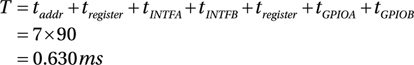
That approach reduces the I2C time to approximately 7-byte times. The total turnaround time can then be reduced to about 0.63 + 0.150 = 0.78 ms.