
Chapter 9: A Better Way to Display – VGA
Up until now, we've been limited to displaying information using LEDs, single color or RGB, as well as the 7-segment display. We are quite capable of performing operations and displaying limited information, as we have demonstrated with our temperature sensor and calculator. The Nexys A7 offers an additional output that can provide us with an almost unlimited method of displaying information, the Video Graphics Array (VGA) connector. The VGA connector on the Nexys A7 can display resolutions of up to 1600x1200, with up to 2^12 or 4,096 colors. What allows us to unlock this capability is that we now know how to use our external memory, which will provide our framebuffer.
By the end of this chapter, we'll have created a method of displaying data on a Cathode Ray Tube (CRT) or LCD monitor via the VGA connector. In Chapter 10, Bringing It All Together, we'll use this methodology to upgrade some of our projects to utilize the new display.
In this chapter, we are going to cover the following main topics using a project, Introducing the VGA:
- Defining registers
- Generating timing for the VGA
- Displaying text
Technical requirements
The technical requirements for this chapter are the same as those for Chapter 1, Introduction to FPGA Architectures and Xilinx Vivado.
To follow along with the examples and the project, you can find the code files for this chapter at the following repository on GitHub: https://github.com/PacktPublishing/Learn-FPGA-Programming/CH8.
A VGA-capable monitor and cable are also required if you want to implement the project on the board.
Project 11 – Introducing the VGA
The earliest professional computer displays were simple monochrome text displays. The earliest personal computers, such as the Apple 2, could display 280x192 pixels with a small number of colors. The Commodore 64 and IBM/PC could display 320x200, again with limited color palettes. The original IBM VGA was introduced in 1987 and it allowed for higher resolutions and standardized the connector going forward until digital displays such as LCDs became the norm.
The first thing we'll need to look at is how the screen is drawn. Whether you are using a CRT display or a modern LCD, the timing is still supported to provide backward compatibility. Originally, the VGA output was designed to drive an electron gun to light up phosphors on a CRT. This meant timing spanned the entire display, plus time for the gun to shift from one side of the screen to the other, or from the bottom back to the top. Figure 9.1 shows the various timing parameters and their relationship to what is displayed on the screen:
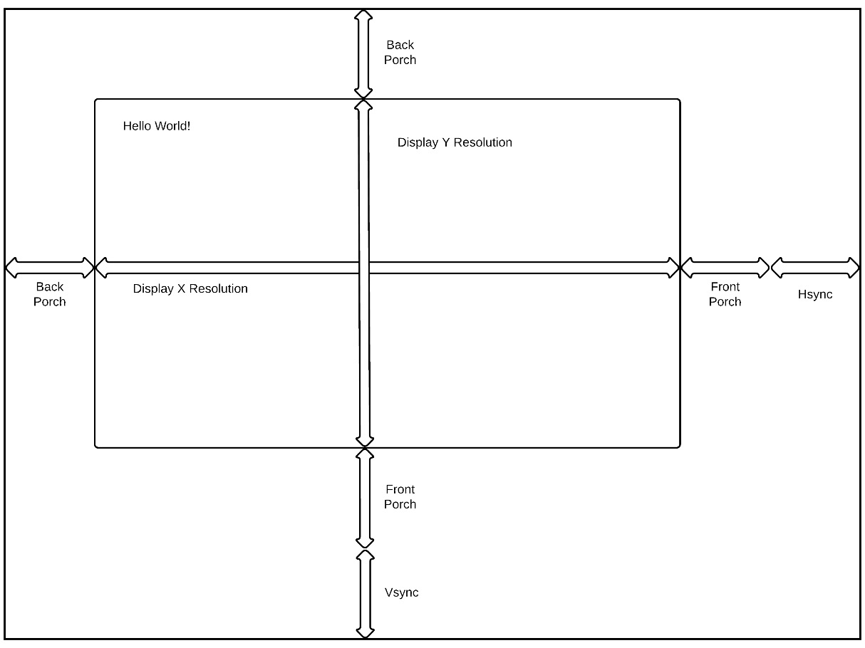
Figure 9.1 – VGA screen timing information as displayed
The main components of the output that we need to generate are as follows:
- Hsync – Horizontal synchronization signal
- Vsync – Vertical synchronization signal
- Red[3:0], Green[3:0], Blue[3:0] – RGB color values. In a real display these would be 8 bits per color (24 bits per pixel (bpp)). However, Digilent opted to create a resistor array implementation of a Digital to Analog Converter (DAC) rather than a true DAC, thereby limiting the bpp to 444 or 12 bpps.
We're going to want to make the VGA controller be as generic as possible. To do this, we'll create a register-based interface, so we'll need to figure out what the values we'll need for a given resolution are.
Important note
The following timing list is fairly comprehensive for a 4:3 aspect ratio display (older CRT/ TV). Depending on the display you use, some of these will not work. We'll default to 640x480 @ 60Hz since this is the base VGA display and should be supported by everything.
We can look at a list of Video Electronics Standards Association (VESA) standards to get an idea of what we want to display:

The preceding table contains the timing for the possible modes our display will support. The first thing to note is that the clock frequency that we'll need varies quite a bit from 25.18 MHz through 195 MHz. We'll address this by introducing clock reconfiguration, which is available in the clocking wizard. We can also make registers for storing the various parameters we'll need, so we'll use an AXI Lite interface for our registers.
Now let's take the relevant numbers from the preceding table and put them into a timing diagram so that we can visualize the actual signals going to the display:
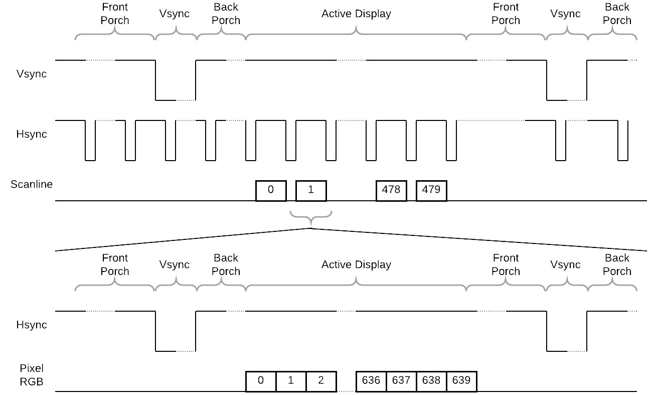
Figure 9.2 – Video timing diagram
In Figure 9.2, we can see how the timing works. The timing is broken up into two sections. The first is the frame time, which can be looked at as the Vsync timing, which is based on the number of scanlines. Each scanline is similarly composed of the Hsync plus data.
To keep things simple, we'll assume that data is stored as 1-bit values. Typically, VGA and VESA modes would have 8-, 16-, or 32-bit colors. 8-bit values would be used as an index into a palette of 256 colors out of 16 million colors. 16-bit colors would typically be 565 or 555 (RGB) values, and 32-bit color was actually 888 RGB values capable of displaying 16 million colors. For our purposes, and since we are tackling quite a bit, I'll keep to storing 1-bit color. A pixel will be on or off.
Important note
When dealing with colors, we'll reference them by the number of bits used to represent them (8, 16, 24, or 32) and the number of bits per color channel (565, 555, or 888), where each digit represents the number of bits used for each color: red, green, and blue.
Defining registers
The first step we'll need for our VGA controller is to define a set of registers we can use to solve our problem. We know the timing parameters from Figure 9.1 and the associated table. From this we can derive some parameters. For our VGA, I would propose the following set:
- Horizontal display start – The number of horizontal pixels before the display starts, equivalent to the horizontal back porch minus one.
- Horizontal display width – The width of the display.
- Horizontal sync width – Hsync width.
- Horizontal display total width – The total width of display and non-display portions.
- Vertical display start – The number of display lines before the display starts, equivalent to the vertical back porch minus one.
- Vertical display height – The height of the visible display.
- Vertical sync width – Vsync height in scan lines.
- Vertical display total height – The total height of the display and non-display portions.
- VGA format – The pixel depth for a given screen.
- Display address – The display address to read from. This can be written at any time, but will not take effect until the beginning of the next frame to prevent tearing.
- Horizontal and vertical polarity selections – Because different modes have active high or low polarities for the sync pulses, we need to provide a way of selecting between them.
- Display pitch – We need to know how many display pages to read for a given scanline as well as how many to count by for each subsequent scanline.
- Load mode – Typically, in complex designs, we may have multiple registers that make up a complete set of values necessary for a given function. We must provide a way to update them all simultaneously once updating is complete.
Our registers will be accessible via an AXI Lite interface.
Coding a simple AXI Lite interface
The write side of the AXI interface involves three components: the address bus, the data bus, and the response bus. We can see the address interface in the core interface definition:
input wire reg_awvalid,
output logic reg_awready,
input wire [11:0] reg_awaddr,
input wire reg_wvalid,
output logic reg_wready,
input wire [31:0] reg_wdata,
input wire [3:0] reg_wstrb,
input wire reg_bready,
output logic reg_bvalid,
output logic [1:0] reg_bresp,
The slave device must be able to handle the address and data buses independently. In our design, we'll write both at the same time, but it's possible that a master device may provide either an address or data before the other. We'll address this in our register state machine:

Figure 9.3 – AXI Lite state machine
Figure 9.3 shows the basic state machine. If awvalid and wvalid are both high, then we can generate the response. If we are missing one of the components to a full transfer, either awvalid or wvalid, we proceed to a wait state and then to the BRESP state.
Finally, in the BRESP state, as soon as we see bready, we generate a success response and transition back to idle.
Now let's examine the actual timing generation.
Generating timing for the VGA
We'll need two Phase Locked Loops (PLLs) or Mixed Mode Clock Managers (MMCMs) for our design. The first PLL will be a duplicate of the one we created in Chapter 8, Lots of Data? MIG and DDR2, to generate clocks for the DDR2 memory controller and also our internal clocks. We will generate the second one so that we can change the timing parameters. By default when the design powers up it will display a VGA resolution of 640x480 @ 60 Hz. The main difference in our configuration is to select Dynamic Reconfig:

Figure 9.4 – Dynamic reconfiguration
Adding dynamic reconfiguration exposes an AXI Lite interface in the clocking wizard that we can use to reconfigure the PLL on the fly. The registers we need to focus on can be found in the clocking wizard drive 6.0 at https://www.xilinx.com/support/documentation/ip_documentation/clk_wiz/v6_0/pg065-clk-wiz.pdf. We'll only be reconfiguring clk0. In the following screenshot, I've extracted the information we need from the clocking wizard. In Figure 9.5, you can see how to extract these numbers yourself:

Figure 9.5 – Extracting reconfiguration parameters
The parameters we need (based on a 200 MHz input clock) are as follows:
- Divide Counter: In Figure 9.5, for 25.18 MHz, this is 9.
- Clock feedback multiplier (Mult Counter) integer: For 25.18 MHz, this is 50.
- Clock feedback multiplier (Mult Counter) fraction: For 25.18 MHz, this is 000.
- Clock feedback divider value integer: For 25.18 MHz, this is 44.
- Clock feedback divider value fraction: For 25.18 MHz, this is 125.
The values can be calculated, but you need to be careful to make sure you don't exceed the maximum PLL frequency. The following table shows the values we need for all our VGA frequencies:

We can use the preceding table to create code to load our pixel PLL. We also need to load the register values for the resolution we need. Let's set that table up first.
First, we'll create a structure to hold the table we'll use to set up the PLL and VGA controller for each of the 17 resolutions that we'll support. We'll create a simple AXI Lite state machine that can configure the desired resolution, but in the future, we could use a microcontroller in the system:
typedef struct packed {
logic [7:0 ] divide_count;
logic [15:8] mult_integer;
logic [25:16] mult_fraction;
logic [7:0] divide_integer;
logic [17:0] divide_fraction;
logic [11:0] horiz_display_start;
logic [11:0] horiz_display_width;
logic [11:0] horiz_sync_width;
logic [11:0] horiz_total_width;
logic [11:0] vert_display_start;
logic [11:0] vert_display_width;
logic [11:0] vert_sync_width;
logic [11:0] vert_total_width;
logic hpol;
logic vpol;
logic [12:0] pitch;
} resolution_t;
The structure encapsulates all the necessary parameters. We can define a variable and initialize it in an initial block to use as constants:
resolution_t resolution[17];
initial begin
// 640x480 @ 60Hz
resolution[0].divide_count = 8'd3;
resolution[0].mult_integer = 8'd21;
resolution[0].mult_fraction = 10'd625;
resolution[0].divide_integer = 8'd28;
resolution[0].divide_fraction = 10'd625;
resolution[0].horiz_display_start = 12'd15;
resolution[0].horiz_display_width = 12'd640;
resolution[0].horiz_sync_width = 12'd96;
resolution[0].horiz_total_width = 12'd799;
resolution[0].vert_display_start = 12'd9;
resolution[0].vert_display_width = 12'd480;
resolution[0].vert_sync_width = 12'd2;
resolution[0].vert_total_width = 12'd524;
resolution[0].hpol = '0;
resolution[0].vpol = '0;
resolution[0].pitch = 13'd5;
We will define all 17 modes in our code. Only the first/default mode is shown here. With this we can now create our state machine to load the VGA and PLL.
The state machine is divided into two sections: CFG_WR0-2 loads the MMCM with our clock configuration settings, while CFG_WR3-5 loads the resolution for the VGA controller. The state machine operates as follows:
- It detects a button press and starts loading MMCM parameters.
- CFG_WR0 checks which valids are active. In the event that only wvalid or awvalid is active, we have two substates, CFG_WR1 and CFG_WR2, to await the missing valid.
- Once both valids are valid, we advance the register write. We must write all 24 registers in the MMCM before we move on to the VGA.
- The VGA portion of the state machine operates similarly to the MMCM portion and we advance through the VGA parameters. Once complete, we go back to idle.
The VGA core handles the monitor timing and the display output.
Important note
Depending on your monitor type, you may not be able to display all resolutions. Some monitors are also more forgiving than others of timing problems. My particular monitor could go to 1280x1024 @ 85 Hz but no higher. Due to timing constraints, I would recommend not going higher than 1280x1024 @ 75 Hz.
Let's now take a deeper dive into the timing generator.
Monitor timing generator
To handle sync generation, we'll need two counters. The first counter, horiz_count, will generate the timing and pixel output for each scanline. The second counter, vert_count, counts the number of scanlines to determine when to start displaying pixels and generate the Vsync:
if (horiz_count >= horiz_total_width) begin
horiz_count <= '0;
if (vert_count >= vert_total_width) vert_count <= '0;
else vert_count <= vert_count + 1'b1;
scanline <= vert_count - vert_display_start + 2;
mc_addr <= scanline * pitch;
mc_words <= pitch;
end else
horiz_count <= horiz_count + 1'b1;
The preceding code zeroes out the horiz_count signal when we reach the end of a scanline. You'll notice that the comparison is a greater than or equal to horiz_total_width signal. The way we update counters doesn't stop or restart the timing generation. This will ensure that if we were to accidently put something out of range, the counts will recover. Similarly, we do the same with the vertical count.
This block also generates a few other parameters we need for displaying pixels. The first is the scanline information. This calculates the scanline currently being operated on. Scanline zero would be the first displayable scanline.
We also register the address for the current scanline and the pitch, which is also the number of 16-byte words to be read for each scanline. Note that this number can be greater than or equal to the number of bytes we need.
It helps when you are using slower parts or trying to achieve a higher clock speed to look for opportunities to precalculate mathematical operations when you can. In the preceding code, I'm calculating the address we need:
mc_addr <= scanline * pitch;
This is because you'll see in the code where we read from memory that we need to make sure we don't violate AXI rules:
vga_hblank <= ~((horiz_count > horiz_display_start) &
(horiz_count <=
(horiz_display_start + horiz_display_width)));
vga_hsync <= polarity[1] ^
~(horiz_count > (horiz_total_width - horiz_sync_width));
vga_vblank <= ~((vert_count > vert_display_start) &
(vert_count <=
(vert_display_start + vert_display_width)));
vga_vsync <= polarity[0] ^
~(vert_count > (vert_total_width - vert_sync_width));
You'll see that we are generating the Hsync and Vsync as shown in Figure 9.1 at the end of the scanline and the display window. We calculate the time to generate this by creating the sync from the horizontal or vertical total minus the sync width. We also need to use our polarity registers to generate the correct sync polarity. Exclusive-OR gates can be used as programmable inverters.
We also generate the blank signals. These aren't technically necessary unless you are using a real DAC, when those signals are used to zero out the pixel output, although you could use them similarly. I've included them since, in simulation, it can assist in locating when data is expected to be output.
In this section of code, we also generate a toggle mc_req signal for requesting data to be displayed:
if (vga_hblank && ~last_hblank && ~vga_vblank)
mc_req <= ~mc_req;
last_hblank <= vga_hblank;
We are taking advantage of the dead time of the display to prefetch the next scanline of data. When hblank is going away, in other words, the rising edge of hblank, we'll generate a request as long as we are not in the vertical blanking period.
Now that we have an operational display, we need something interesting to display on it.
Displaying text
A text character in its oldest and simplest form is a bitmap. Modern operating systems may use things such as TrueType, which can scale cleanly and easily at different resolutions. However, the oldest form of displaying text was to store a pattern in memory and then copy it to the screen.
I've included a file called text_rom.sv. It is essentially a lookup table:
module text_rom
(input clock, // Clock
input [7:0] index, // Character Index
input [2:0] sub_index, // Y position in character
output logic [7:0] bitmap_out);
Functionally, we can view the text ROM in the following diagram:
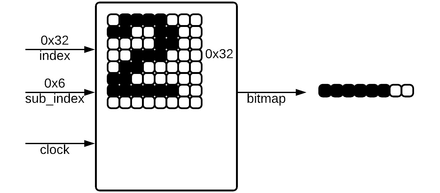
Figure 9.6 – text_rom
Every clock cycle, a character is looked up using the index and the subindex references the scanline of the character. In Figure 9.6, you can see an example where we are requesting character 0x32, which is American Standard Code for Information Interchange (ASCII) for the number 2. We are asking for the sixth scanline of the character. This returns the value 0xFC on the next cycle, which represents the pixels from the sixth scanline of the number 2.
Important note
ASCII code is one of the major standards for encoding text. One nice thing about ASCII is that the numbers 0-9 are encoded from 0x30-0x39.
text_rom.sv contains all the ASIC uppercase and lowercase characters and numbers as well as a few fill characters. ASCII is normally represented by an 8-bit value, so there is plenty of room to add new characters to display:
always @(posedge clock)
case ({index, sub_index})
…
// 2
{8'h32, 3'h0}: bitmap <= 8'h78;
{8'h32, 3'h1}: bitmap <= 8'hCC;
{8'h32, 3'h2}: bitmap <= 8'h0C;
{8'h32, 3'h3}: bitmap <= 8'h38;
{8'h32, 3'h4}: bitmap <= 8'h60;
{8'h32, 3'h5}: bitmap <= 8'hC0;
{8'h32, 3'h6}: bitmap <= 8'hFC;
{8'h32, 3'h7}: bitmap <= 8'h00;
Here we can see what the lookup for the number 2, 0x32, looks like. This is the same as what is represented in Figure 9.6.
One thing about the way data is stored is that in the application I developed, we'll need to flip the data coming out. I've added the following code:
always @* begin
for (int i = 0; i < 8; i++) begin
bitmap_out[i] = bitmap[7-i];
end
end
This code flips the bits. Without it the text will appear reversed. You may or may not need this for your own applications, so it's good to know it exists in the event you need it or need to remove it.
Back to our top-level VGA. We'll add a string of text with each resolution setting so that when the display is set, we can print out what we have set it to:
res_text[0] = " zH06 @ 084x046";
Notice that the text is written backward as a string. This is because we are starting from bit 0 of character 0 and building it up to character 15, bit 7.
Requesting memory
For our display, we need to take our memory request signal and synchronize it to the memory controller clock. We'll also use this opportunity to reset the pixel FIFO. Note that we are toggling the request signal at the end of the line, so this provides a couple of key features for our design:
- We won't be displaying anything, so we can simply reset the FIFO.
- We should have quite a bit of time to reset the FIFO and start getting data back for displaying.
We can construct a state machine to handle our memory accesses as shown in the following code block:
case (mem_cs)
MEM_IDLE: begin
mem_arvalid <= '0;
if (^mc_req_sync[2:1]) begin
fifo_rst <= '1;
mem_cs <= MEM_W4RSTH;
end
end
MEM_W4RSTH: begin
next_addr <= mc_addr + mc_words;
len_diff <= 2047 - mc_addr[10:0];
if (wr_rst_busy) begin
fifo_rst <= '0;
mem_cs <= MEM_W4RSTL;
end
end
When we synchronize and detect an edge on the request, we reset the FIFO. The FIFOs provide an output to indicate when they are busy during a reset, so in the second state, we wait for the reset to go high, then release the reset, and enter the state to wait for it to go low again. We can take advantage of our wait time to calculate the next address and see how many scanlines there are before we reach the 2K (2,048) byte boundary.
Important note
When making a burst request over AXI, you cannot cross the 2,048-byte boundary. We must take this into account and break up bursts that might possibly violate this rule.
We'll use these parameters to test for a boundary crossing in the following code block:
MEM_W4RSTL: begin
if (~wr_rst_busy) begin
// Make a request from the current address
mem_araddr <= mc_addr;
if (next_addr[31:11] != mc_addr[31:11]) begin
// look if we are going to cross 2K boundary
mem_arlen <= len_diff;
if (mem_arready) mem_cs <= MEM_REQ;
else mem_cs <= MEM_W4RDY1;
end else begin
// Make a single request
mem_arlen <= mc_words - 1;
if (mem_arready) mem_cs <= MEM_IDLE;
else mem_cs <= MEM_W4RDY0;
end // else: !if(next_addr[12])
// Calculate the parameters for second request
next_addr <= mc_addr + len_diff + 1'b1;
len_diff <= mc_words - len_diff;
end
end // case: MEM_W4RSTH
When the reset goes away, we can make a request to the memory controller. We have already calculated the next address, so we can test the upper bits to see whether the next address falls into the next 2,048-byte page. Based on the test, we'll either make a single request or a request for the last part of the current 2,048-byte page. In either case, we can move directly to the second request or back to IDLE if the awready signal is high, otherwise we need to move to a state to wait for awready.
We'll also pre-calculate the address and length of the second request in the event we need it:
MEM_REQ: begin
if (~wr_rst_busy) begin
mem_araddr <= next_addr;
mem_arlen <= len_diff;
if (mem_arready) mem_cs <= MEM_IDLE;
else mem_cs <= MEM_W4RDY0;
end
end // case: MEM_W4RSTH
The final state handles the remainder of the scanline if it crossed the 2,048-byte boundary.
To handle the data coming back, we'll use a Xilinx async, xpm_fifo, as shown in the following code block:
// Pixel FIFO
// large enough for one scanline at 1920x32bpp (480 bytes)
xpm_fifo_async
#(.FIFO_WRITE_DEPTH (512),
.WRITE_DATA_WIDTH (128),
.READ_MODE ("fwft"))
u_xpm_fifo_async
(.rst (fifo_rst),
.wr_clk (mem_clk),
.wr_en (mem_rvalid),
.din (mem_rdata),
.wr_rst_busy (wr_rst_busy),
.rd_clk (vga_clk),
.rd_en (vga_pop),
.dout (vga_data),
.empty (vga_empty),
.rd_rst_busy (rd_rst_busy));
The main things to observe regarding the FIFO is that we are writing on the memory clock and reading on the VGA pixel clock. In this design, I haven't taken any precautions to make sure the data is loaded for a scanline or to handle exceptions. This results in the memory reads being fire and forget. We have a state machine that makes the request and the data is pushed back into a FIFO to be read out.
The FIFO is configured as first-word fall-through (fwft), which means the data is ready on the output for immediate use.
Finally, we need to read from the FIFO and display on the screen:
initial scan_cs = SCAN_IDLE;
always @(posedge vga_clk) begin
vga_pop <= '0;
case (scan_cs)
SCAN_IDLE: begin
if (horiz_count == horiz_display_start) begin
if (vga_data[0]) vga_rgb <= ~vga_empty;
else vga_rgb <= '0;
scan_cs <= SCAN_OUT;
pix_count <= '0;
end
end
SCAN_OUT: begin
pix_count <= pix_count + 1'b1;
// Right now just do single bit per pixel
if (pix_count == 126) begin
vga_pop <= ~vga_empty;
end
if (vga_data[pix_count]) vga_rgb <= '1;
else vga_rgb <= '0;
if (rd_rst_busy) scan_cs <= SCAN_IDLE;
end
endcase // case (scan_cs)
end
The display state machine is pretty simple. We wait until we reach the first scanline and then, based on the pixel format, we can display on the screen. This version of the code only supports 1 bpp.
At this point, we can run on the board and we should see VGA output. We've initialized the core to run at 640x480 @ 60 Hz:

Figure 9.7 – First VGA screen attempt
I've fixed this problem in the code you are running. Without a startup clearing of the memory, we are at the mercy of old data or data from the memory controller initialization being displayed:
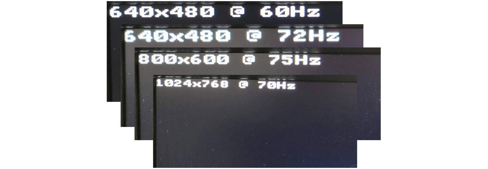
Figure 9.8 – Sample resolutions
When you first bring up the project, it will clear the screen and display 640x480 @ 60 Hz. This is accomplished by one state that is only executed when powering on:
CFG_IDLE0: begin
update_text <= ~update_text;
cfg_state <= CFG_IDLE1;
end
We've now completed a simple, yet useful, VGA controller. I hope when looking at this that you can see that writing hardware that is useful isn't out of reach. Certainly, there is a lot of work that goes on behind the scenes in order to make sure it works for what you want.
Testing the VGA controller
Most of the testing was done on the board. The turnaround time for a compile is short. The simulation time for a full frame is very long using the Vivado Simulator due to the PLLs and the memory controller. It is, however, a good way to check the first few scanlines of a display to make sure they look okay and that the timing works alright.
The two main pieces that we need for simulating are the clock generator and the register load:
initial clk = '0;
always begin
clk = #5 ~clk;
end
…
initial begin
SW <= 8;
button_c <= '1;
repeat (1000) @(posedge clk);
while (~u_vga.init_calib_complete) @(posedge clk);
$display("DDR calibration complete");
while (~u_vga.locked) @(posedge clk);
button_c <= '1;
repeat (100) @(posedge clk);
button_c <= '0;
repeat (10000) @(posedge clk);
end
A more complete testbench could contain tasks for saving video frames, but given the speed, you are better off running on the board. To run on the board, we need to examine the constraints necessary.
Examining the constraints
In the VGA we have quite a bit of clock domain crossing to handle. The FIFO handles the data, but we have data going from our AXI interface to our memory controller clock and then to the VGA display clock. On top of this, we have a variable frequency VGA clock from the programmable MMCM.
When you implement an MMCM or PLL, Vivado will automatically create a generated clock on the output. Since we will reprogram the PLL during operation, we'll need to override this with the maximum clock we expect to see during operation:
create_clock -period 7.41 -name vga_clk -add [get_pins u_clk/clk_out1]
We'll also need the clock periods for setting up the following constraints. We can get the period parameter from a clock by using get_property. get_clocks can be used to access the clock information:
set vga_clk_period [get_property PERIOD [get_clocks vga_clk]]
set clk200_period [get_property PERIOD [get_clocks clk_out1_sys_clk]]
set clkui_period [get_property PERIOD [get_clocks clk_pll_i]]
Experimenting a bit, I was able to discover that we could reliably run up to about 135 MHz, so I provided this as a clock on the PLL output.
Now we need to add constraints for our synchronizer inputs. Since these are single signal toggle synchronizers, we'll false-path the input to the first stage of the synchronizer flip flops:
set_false_path -from u_vga_core/load_mode_reg*/C -to */load_mode_sync_reg[0]/D
set_false_path -from u_vga_core/mc_req_reg*/C -to */mc_req_sync_reg[0]/D
set_false_path -from update_text_reg/C -to update_text_sync_reg[0]/D
We'll also add in max_delay constraints to make sure to properly constrain the registers between clock domains and to not push the tool to meet unreasonable timing requirements. We do this as follows:
set_max_delay -datapath_only -from */horiz_display_start_reg* [expr 1.5 * $vga_clk_period]
set_max_delay -datapath_only -from */horiz_display_width_reg* [expr 1.5 * $vga_clk_period]
…
set_max_delay -datapath_only -from *sw_capt_reg*/C [expr 1.5 * $clkui_period]
set_max_delay allows us to set the amount of time from any point to any other point. -datapath_only tells the timing engine to not consider clock delays in computing the delays.
With this we have implemented our design on the board and met timing. In the next chapter, we'll add in a keyboard and use the VGA as a capstone project where we can use it to display data from our previous projects.
Summary
In this chapter, we've introduced a better way of displaying data. Previously, we were limited to the physical outputs: a row of 16 LEDs, two tricolor LEDs, and the 7-segment display. We made good use of them for the simple testing of logic functions, our traffic light controller, and our simple calculator. We've used a ROM to display text. We've introduced a programmable PLL and used our DDR2 controller. We're now ready to tackle our capstone project.
In the next chapter, we'll wrap up the book by putting everything together. We can use our VGA to display the output from our temperature sensor, calculator, and microphone. We'll also introduce the PS/2 keyboard interface to provide an easier way to control the system.
Questions
- You can use an XOR gate as:
a) A way to add two bits
b) A way to multiply two bits
c) A programmable inverter
- We are limited to what resolution when generating a VGA controller?
a) 640x480 @ 60 Hz
b) 1280x1024 @ 85 Hz
c) 1920x1200 @ 60 Hz
d) A resolution our monitor can handle and a pixel clock that we can reliably meet timing for in our design
- Building a VGA controller in an FPGA is impractical.
a) True
b) False
- How many colors can we represent with 888 or 24 bpp?
a) 2 colors
b) 16 colors
c) 64K colors
d) True color, or 16 million colors
- An AXI Lite write interface consists of which of the following?
a) A write address
b) Write data
c) A write response
d) All of the above
- An AXI Lite read interface consists of which of the following?
a) A read address
b) Read data
c) A read response
d) All of the above
e) (a) and (b)
Challenge
The current VGA design only displays black and white. Can you change the design to display two different colors? Can you modify it to use some switches on the board to select these colors?
Further reading
For more information about what was covered in this chapter, please refer to the following links: