Schematic Capture
You are probably very familiar with various schematic symbols and diagrams. A schematic is merely a collection of electronic symbols connected together with virtual “wires.” The main reason you need a schematic when fabricating a printed circuit board is to provide input (a netlist) to your layout and routing tool. A netlist is a file, usually ASCII text, which defines the connections between the components in your design. Other uses for a schematic when fabricating boards include documentation, archiving, and the automatic generation of a bill of materials (BOM).
If your design is simple, you may not need to generate a schematic and it is possible to skip this step and proceed directly to layout and routing of the circuit board. However, you may still need to generate a netlist to feed to the layout tool.
The Schematic Symbol
For most circuits, a photograph or realistic drawing showing actual components and their interconnections would be far too complex to be of value in replicating the circuit. A schematic symbol is a simplified representation of a real-world component. A schematic diagram shows such representations of real-world components and a simplified “map” of how they are connected together. It would be silly to tape resistors and capacitors to a piece of paper, so instead we use drawings that represent those parts.
Schematic symbols come in all sizes and shapes. They can be as simple as stick figures or as complicated as a work of art, but they all have a few common features. These features are summarized below:
1) Each symbol contains a graphic, or drawing, that represents the part or its function. The graphic is usually referred to as a component body. In the examples shown in Figure 1-1 the graphics show a resistor, a capacitor, a diode, and an integrated circuit.

2) Each symbol needs to have a name that the schematic tool can refer to. This name is usually referred to as a component name. A component name for a symbol is similar in function to a file name for a file.
3) The component body also has lines coming off it called pins that represent the connections to the part itself.
4) Each pin has a unique pin number assigned to it. There should not be duplicate pin numbers on a single component. For example, the resistor shown should not have two pins numbered “2.”
5) Each pin can have a name assigned to it. Each name should be unique for the symbol in question. The LM317 shown above has pin names associated with each pin.
6) Each symbol has a reference designator assigned to it in order to uniquely identify it from other symbols in the schematic. The schematic and layout tools typically use the reference designator to uniquely identify components in a design. The example reference designators shown are R1, C1, D1, and U1. Normally the reference designator is a letter (or letters) followed by a number. Duplicate reference designators should not be used in the same design.
Symbol Properties
Pin numbers, pin names, component names, etc. are referred to as properties. There are many other properties that can be attached to a symbol, such as part number, package name, manufacturer, description, etc. You can make up your own property names to suit your own individual goals. Whether you use these properties depends on whether your schematic capture tool can support them, how much detail you want on your schematic, and what your schematic and layout tools require. (For instance, most layout tools require a property that defines the component package type.)
After many years of generating schematics, I have come up with a list of properties that I feel properly describes a component. I consider these properties to be “musts.” These properties and their descriptions are listed below. However, keep in mind that your schematic or layout tool may require other properties not listed below:
![]() Part Number: Describes the actual part number of the component (for example, “1N4148DICT”). If your schematic capture tool supports bill of materials (BOM) generation, this is what will be listed.
Part Number: Describes the actual part number of the component (for example, “1N4148DICT”). If your schematic capture tool supports bill of materials (BOM) generation, this is what will be listed.
![]() Component Name: This is the name of the symbol from the schematic capture tool’s point of view. Think of it as a file name for a symbol, such as “resistor,” “resistor_surface_mount,” or “diode.”
Component Name: This is the name of the symbol from the schematic capture tool’s point of view. Think of it as a file name for a symbol, such as “resistor,” “resistor_surface_mount,” or “diode.”
![]() Reference Designator: Describes the reference name that the schematic and layout tools will use to identify the part. For example, you could place four resistors on a schematic. Each symbol may have the same component name (resistor_through_hole_.25w), but each will have a different reference designator (R1, R2, R3, and R4). Each symbol in a schematic must have a unique reference designator.
Reference Designator: Describes the reference name that the schematic and layout tools will use to identify the part. For example, you could place four resistors on a schematic. Each symbol may have the same component name (resistor_through_hole_.25w), but each will have a different reference designator (R1, R2, R3, and R4). Each symbol in a schematic must have a unique reference designator.
![]() Package Name: Describes the component’s package type or footprint (for example, “DIP16” or “PLCC44”).
Package Name: Describes the component’s package type or footprint (for example, “DIP16” or “PLCC44”).
![]() Value: Describes the component specifics, such as resistance or capacitance values, such as “240 ohms” or “40pf_10v.” Not all symbols will need this property.
Value: Describes the component specifics, such as resistance or capacitance values, such as “240 ohms” or “40pf_10v.” Not all symbols will need this property.
The following properties are not required but are nice to have:
![]() Manufacturer: Describes the manufacturer of the component for creating a bill of materials (BOM) for use when ordering components.
Manufacturer: Describes the manufacturer of the component for creating a bill of materials (BOM) for use when ordering components.
![]() Description: Describes the part to make it easier for others to understand (for example, “3:8 multiplexer”).
Description: Describes the part to make it easier for others to understand (for example, “3:8 multiplexer”).
Not every schematic tool will support all of the properties described above. You need to understand your schematic tool fully in order to decide which properties to use. Go through the examples and tutorials that come with your schematic and layout software to help you decide which properties are right for your application.
Schematic Generation
The first step in generating a schematic is to create symbols for all the components. The exact details of this process will vary with the schematic capture tool you choose. Most of the work prepared for this book was done with SuperCAD and SuperPCB by Mental Automation (see the resource list in Chapter 7). Once all the symbols are created, place or instantiate them on a blank schematic page or pages. It is a good idea not to fill the page up too tightly because you will not have room to add the wires, or connections, and any other parts you may decide you need later. Figure 1-2 shows a schematic with all the symbols instantiated but not connected. In this example, all the components fit on a single sheet. If you need more than one sheet, don’t worry. Almost all of the schematic and layout tools can handle schematics drawn on multiple sheets. You can also increase the size of a single sheet if you prefer only one but this can make it difficult to handle, print and store.
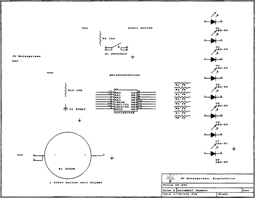
Once you have the symbols instantiated, it is time to start connecting them with “virtual wires.” These “wires” are nothing more than lines drawn between the pins of the symbols. The schematic tool knows that these lines represent physical connections between the components. Figure 1-3 shows the same schematic with the connections completed. The exact details that you will follow will again vary with the schematic capture tool you choose. With all of them, however, it is as simple as activating the wire tool and clicking and dragging with the mouse.

For schematics with multiple sheets you will probably have to run wires, or nets, to other sheets. This is done with the net name property. Simply name the net on the first sheet, and then name any other nets on any other sheets that you want connected with the same name. The schematic tool will connect all nets with the same name. For example, a net named LED_ENABLE on one sheet will be electrically connected to all other nets in the design with the same name. Some schematic tools require you to place off page connectors on nets that leave and enter schematic sheets.
You should note that once a net has been named all other nets with that same name are connected together. Note that in Figure 1-3 there are three nets with the name VCC. All these nets are connected together even though there is no wire connecting them. Sometimes this is known as a virtual connection. This helps to keep any unnecessary clutter on a schematic sheet to a minimum. Note that you do not have to name all of the nets in a schematic. The nets that you do not name will have a name assigned to them by the schematic tool. However, assigning names to all critical or important nets now will make it easier to refer to them when you are error checking the design, and later on when you are placing and routing the design.
You may have noticed that there are a few pins missing from the microcontroller, U1, shown in the previous figures. Specifically, those pins represent power and ground connections. Almost all integrated circuits contain power and ground connections that connect to a common supply rail such as VCC and GROUND. Why bother to add these pins to your symbols and clutter up the schematic? SuperCAD allows you to identify certain pins on a symbol as power and ground pins when you create the symbol. All power pins are connected to a power supply rail named VCC, and a ground rail named GROUND. SuperCAD automatically keeps track of these connections for you so you don’t have to. In the schematic shown in Figure 1-3, the power connections to VCC and GROUND are implied for the microcontroller U1. However the connections are explicitly shown for the battery connector B1. Although not recommended, you can mix and match embedded and explicit power pins in a design.
This is a very nice feature, but beware! What happens if you have multiple power supply rails in your design, or you need separate analog and digital ground connections? Most schematic tools have some way in which to handle this but we would recommend adding the power and ground pins to your symbols and connecting them up explicitly. In fact, for most of the designs I’ve done, I’ve added all power and ground pins to the symbols so that their connections are obvious to all who look at the schematic. It also makes reviewing the design easier later on.
Once the schematic is complete you need to run a schematic design rule checker. Notice I said “need,” not “should.” Checking your design is a must. Design rule checkers vary greatly from schematic tool to schematic tool but they all try to do the same thing. They can look for unconnected nets, commonly referred to as dangling nets. They can look for shorted nets, unconnected pins, duplicated pins on a symbol, etc. Some tools like SuperCAD can also look for conflicts such as two or more output drivers on a single net, or no output drivers on a net. Read the documentation that came with your schematic tool.
Notice the comments placed on the schematic shown in Figure 1-3. These comments are not necessary but they will help you and anybody else who sees your schematic to understand it. Comments are free, so use them!
Generating a Netlist
Now that you have created a schematic, what do you do with it? Whether you know it or not, one of the main reasons for creating an electronic schematic was to help you with the placement and routing of the printed circuit board. (Not to mention giving your kids a lot of scrap paper to color on!) Once your schematic is complete and has passed all of the rules checking required by your schematic capture tool, you can generate a netlist. This netlist is usually an ASCII (text) document defining the connections shown in your schematic. This netlist is used by the layout tool help route your board.
The netlist for the schematic shown in Figure 1-3 is shown below. It was created with SuperCAD by Mental Automation.
Netlist for design: C:JV_ENTPCBCTCT
def16———u1-4i,r9-2z,s1-1u,s1-2u
Vcc———u1-14,r9-1z,b1-1u,b1-2u,r10-1z
GROUND———u1-5,d1-2b,d8-2b,d2-2b,d3-2b,d4-2b,d5-2b,d6-2b,d7-2b,u1-3i,b1-3u,&
A typical netlist usually contains a header that lists the name of the design, time and date stamps and some various statistics such as total number of nets, processing time, etc. The main body of the netlist file contains all the connection information. For nets that do not have specific names, the schematic tool assigns names to them. That is what all the def# names in the above file are. After the net name, all of the pins connected to it are listed. For example net def5 consists of pin 1 of R2 and pin 7 of U1. This information will be fed to the layout tool to help insure that the circuit board traces match the schematic connections. If you were really ambitious, you could have created the above netlist by hand and saved the cost of the schematic tool but this really isn’t a good idea.
It may look easy for simple designs, but for others with many pages and many more symbols the task will be immense and prone to errors.
You may notice other items in the netlist, such as the letters z,u,i and others. These letters define the direction of the pin in question. For example U1-3i tells us that Pin 3 of U1 is an input. Alternatively other pins may be defined as outputs (o), bi-directional (b), analog (a), or undefined (z). SuperCAD uses these directions to help check the design for errors. For example, there should not be a net in the design with more than one output connected to it. If you had the outputs of two logic gates connected together and one was a logic high while the other was a logic low, what would the state of that net be? After a while the state of that net would be broken! You also would not want a net without any outputs on it. The state of that net would be undefined (and probably useless). Each schematic tool handles these types of error checking differently. You should read the documentation that came with your software to determine just what kind of error checking, if any, your tools perform.