Placement and Routing Considerations for Various Circuit Designs
Placement and Routing Considerations for General-purpose Analog Circuit Boards
A “general-purpose” analog circuit board is defined here as one that uses common analog circuitry (op amps, transistors, etc.) that operates at only a few megahertz (MHz) of bandwidth. This type of circuit is fairly forgiving of circuit board placement and routing oversights, but there are a few guidelines still to be followed. Proper ground and power distribution (as described in Chapter Two) is important, as are decoupling capacitors. Beyond that, you should not have many problems.
Placement and Routing Considerations for General-purpose Digital Circuit Boards
“General-purpose” digital circuit boards contain digital circuitry (gates, counters, microcontrollers, etc.) that operates up to about 20 MHz. There is usually not much critical timing in the design. Once again, this board type is fairly forgiving of placement or routing oversights. Since the circuitry on the board is digital, however, there are a few other things to think about when placing and routing your board.
Most modern digital circuitry is CMOS (complementary metal oxide semiconductor) of one type or other, rather than the older TTL (transistor-transistor logic). CMOS logic consumes much less power and switches faster than TTL. The increased speed comes with a price, however; the price is noise! The extremely fast transitions on CMOS logic outputs—1 nanosecond (ns) or less—produce much more power supply noise and crosstalk than TTL logic.
To prevent CMOS logic from corrupting your power supply, be sure to use appropriate decoupling capacitors. As a minimum, you should have one capacitor (0.1 μF ceramic is typical) per CMOS chip. Place the capacitor close to the chip’s power pin, as described in Chapter Two. Devices with more than one power pin need more than one decoupling capacitor; one decoupling capacitor per power pin is sufficient.
Controlling crosstalk on a general purpose digital circuit board is usually not too difficult. Be sure not to route outputs next to inputs, especially if the inputs are to be used when the outputs are switching. This will prevent the sharp transition of the output from coupling onto the input line at just the wrong time. Of course, it is impossible to route the board without getting inputs and outputs close together somewhere; just try to avoid long lines where the coupling might be worse.
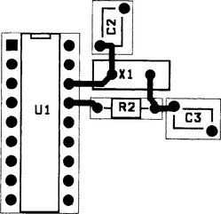
One final note about general-purpose digital circuitry involves crystal oscillators. Most microcontrollers use a crystal oscillator as a timing reference. The crystal is used in a positive feedback loop around an amplifier in the microcontroller. The positive feedback makes the amplifier unstable, so it oscillates. If everything goes right, the amplifier oscillates at exactly the frequency of the crystal. Who cares, you ask? Well, you do! If you are faced with a board design containing a crystal oscillator, you must be careful both with placement and with routing. Most crystal circuits require a small capacitor (typically a 15-pF ceramic) to ground on each side of the crystal. In addition, some circuits have a resistor in series with the feedback loop. To insure that your oscillator will work, place it first (right after the microcontroller). Try to place the crystal and resistor in a small loop, right next to the pins of the microcontroller. Place the startup capacitors close by. Route the board with the shortest routes possible, and make sure the ground connections on the capacitors are very short. See Figure 3-1 for a correctly placed and routed crystal oscillator. Notice how X1 (the crystal) is in a small loop of traces starting and ending at U1 (the microcontroller). R2 (the series resistor) is in the loop, while C1 and C2 (startup capacitors) are connected from the two loop nodes to a ground plane (not shown). Notice how the parts are placed as close together as possible, and how the traces form a small, tight loop.
Placement and Routing Considerations for High-performance Analog Circuit Boards
“High-performance” analog circuit boards contain analog circuitry that is either higher in bandwidth (like video circuitry), higher in gain (like sensor amplifiers), lower in noise, or have larger dynamic range (like A/D and D/A converters) than a general-purpose analog circuit board. No matter what type of circuitry is on your board, there are a few useful techniques for placing and routing high-end analog circuitry. By this point, it should go without saying that good grounding, power distribution, and decoupling techniques must be used.
The active devices (op amps and transistors) on a high-performance board tend to have both more gain and operate at higher frequencies. This can yield significant problems if a few guidelines are not followed:
![]() Be sure that amplifier outputs and inputs are separated.
Be sure that amplifier outputs and inputs are separated.
![]() Be sure that op amp feedback loops are physically small. Place feedback resistors and capacitors as close as possible to the op amp pins.
Be sure that op amp feedback loops are physically small. Place feedback resistors and capacitors as close as possible to the op amp pins.
![]() Remember to always put a small capacitor (100-pF ceramic) in parallel with the op amp’s negative feedback resistor to reduce gain at high frequencies, where oscillations usually happen.
Remember to always put a small capacitor (100-pF ceramic) in parallel with the op amp’s negative feedback resistor to reduce gain at high frequencies, where oscillations usually happen.
![]() If you have a large amount of gain from multiple devices in series, make sure that the output device is far from the input device.
If you have a large amount of gain from multiple devices in series, make sure that the output device is far from the input device.
![]() If you have a large amount of gain from multiple devices in series, make sure that the input and output devices are not in the same package. In this case, it is often better to use two dual op amps instead of one quad op amp.
If you have a large amount of gain from multiple devices in series, make sure that the input and output devices are not in the same package. In this case, it is often better to use two dual op amps instead of one quad op amp.
In addition to these guidelines, the performance of analog circuitry can be improved by a technique called ground rings. A ground ring is used to isolate a section of circuitry from the rest of the board. It is most useful for high-end op amps. See Figure 3-2 for an example of a ground ring. See how the ground ring surrounds the sensitive input pins of the amplifier. It connects both to the ground pins of the amplifier and to the ground plane of the board (not shown). Ground rings should be used on low noise or high impedance points in the circuit.

Another important routing technique involves differential signals. These signals are often used to improve a system’s dynamic range and noise immunity. A differential analog signal is actually a pair of signal lines with opposite DC values. In a typical differential signal application, a pair of differential signal lines is used to move a signal from a driver to a receiver. Note that these parts can be quite a distance from one another. The differential driver (usually built from an op amp) drives each signal line in opposite directions. At the other end, the differential receiver (also usually an op amp) subtracts the two signal lines from each other to produce the output signal. When routing these types of signals, it is important that the two lines be routed completely parallel and close to each other. The reason for this is so that any external noise will be coupled equally onto each line, and thus subtracted out at the receiver. This is one of the only times when long parallel routes can actually work to your advantage.
Placement and Routing Considerations for High-speed Digital Circuit Boards
This type of board has digital circuitry that runs above 20 MHz. Common components in this type of design include microprocessors or digital signal processors, static or dynamic RAM, flash memory, high-speed programmable logic, and complex mixed signal processors. There is often critical timing in the design, where signals must arrive within one nanosecond (ns) of each other. These designs also usually have large (more than eight bits) address and/or data busses which must be connected between chips.
The high-speed operation of these large busses creates tremendous electrical noise. When 16 or 32 CMOS lines change state simultaneously, a large amount of energy is required from the power supply. The supply cannot provide the power fast enough, because of the inherent inductance in even the best-designed distribution system. For this reason, power supply decoupling is even more important. Every pin which connects to the power supply must have a decoupling capacitor (0.1 μF ceramic is typical). This means that, for a microprocessor or DSP chip, there may be as many as 20 decouplers! In addition to the 0.1 μF decouplers on each power pin, you should provide a “bulk” decoupling capacitor for each large digital device. This is usually a larger capacitance (10 μF tantalum is typical) to provide an energy store for this hungry digital chip!
Be careful when you route the decoupling capacitors. In order to prevent the noisy chip from corrupting your power supply, you must make sure that the capacitor is located between the chip and the supply. Figure 3-3 shows a poorly placed and routed decoupling capacitor, while Figure 3-4 shows a correct decoupling design.


In both Figure 3-3 and Figure 3-4, U1 is the active device. It connects to the power supply on pin 14, and the power is provided by connector BT1. C1 is the decoupling capacitor. Notice how in Figure 3-3 the power flows in from BT1 directly into U1, while C1 is way off to the right. In fact, as far as high-frequency noise is concerned, C1 is effectively out of the circuit. The long trace length between U1 pin 14 and C1 will contribute enough stray (parasitic) inductance such that the effective value of C1 is greatly reduced. Now consider the circuit in Figure 3-4. In this case, the power must flow in from BT1, through the input pin of C1, and into U1 pin 14. In this case, C1 will effectively decouple any high frequency noise produced by U1. Note that the idea here still applies no matter how the power is applied to the active devices. In the examples, I used connector BT1, but you might use a trace, or a via, from a backside or inner power layer. No matter how the power gets to the chip, it should have to go through the decoupling capacitor and from there through a short trace directly to the device power pin. You cannot decouple a circuit board too well.
When routing the high-speed digital circuit board, keep all routes as short as possible. If the route lengths get too long, the fast logic transitions may cause signals to bounce back and forth up and down the route, causing ringing on the desired signal. This ringing is also called a transmission line effect. The signal ringing can be reduced by terminating the routes with a resistor. A shunt termination is often used. This is usually a “pullup” (to the power supply) or a “pulldown” (to ground) resistor of approximately 10 kilohms. The shunt termination is placed at the destination of the route. Keep in mind that the shunt termination will dissipate power and load the logic gate that is driving the line.
In some cases, a shunt termination may not be enough to reduce the ringing to acceptable levels. This is often true of high-speed clock lines. In these cases a series termination will usually reduce transmission line effects to tolerable levels. The series termination is usually a small resistor (150 Ω typically) placed at the source of the signal.
High-speed digital clocks are among the most difficult signals to route. A common problem is how to distribute a clock from some type of source (an oscillator or gate output) to several different inputs across the board. There are basically two ways to do this: a “starburst” or a “daisy-chain” route. The starburst route places the clock source in the center of a “star,” with each clock load at the end of a route. The problem here is that each arm of the star is a transmission line. If these lines aren’t terminated correctly, the reflections and ringing will all combine at the center of the star, and can ruin the clock signal. If you do terminate each end of the star, the clock source may not have enough power to drive all of the terminations.
The other solution is to route the clock signal in a daisy chain. This is a single, long route from the source, through each load one by one. The line should be terminated at the end to avoid ringing. This is a more difficult way to route the clock, but will often give superior results.
Placement and Routing Considerations for RF Circuit Boards
Radio frequency (RF) circuit boards are generally considered the most difficult boards to place and route. This is due to the characteristics of the circuits and signals found in typical radio designs. Signals on an RF board range in frequency from zero (DC) to tens of gigahertz (10,000,000,000 cycles per second!). In addition, the amplitude (size) of the signals ranges from tens of nanovolts (0.00000001 volt) to tens of volts. Circuits commonly used in RF designs often have very high impedance. This, combined with the high gain commonly found in radio designs (a gain of 100 dB, which is ten billion, is not unusual!), greatly increases the circuits’ susceptibility to interference or pickup. Finally, the component values used in RF circuits are often very small. Capacitors as small as 0.1 pF (0.0000000000001 farad) and inductors as small as 10 nH (0.00000001 henry) are commonly used. All of these factors combine to make an RF circuit board a true placement and routing challenge. A good RF board designer must keep each of these difficulties in mind as he or she places and routes the board. Note that I said “he or she,” not “it.” There is no place for automatic placement or routing software in the design of RF circuit boards. If you think you will save time by using these tools, then think again. You will only force yourself to completely redo the board (by hand) after it doesn’t work!
RF Circuit Board Special Placement Considerations
It has been said that the three most important factors in real estate are “location, location, and location.” That may or may not be true, but it is definitely true that the three best ways to design an RF circuit board are “placement, placement, and placement”! No amount of clever routing or grounding will make an incorrectly placed RF board function well.
When placing the board, start at one end of the schematic (like a radio receiver’s antenna) and work towards the other end (such as the speaker). It is often best to work from high frequency to low; in this way you place the most critical components first. As you go, place active devices (ICs or transistors) first, then place any passives that are directly in the signal path. Next place any decoupling capacitors or choke inductors. Ignore (for now) any other components. This way you can place the RF signal chain first and fill in any support or control components later.
As you place the signal chain, think about the function and frequency of each device. Do not place active devices near each other that have high gain, or that operate in the same frequency band. For example, if one chip is a receive IF strip with a high gain (maybe 80 dB) at 45 MHz, and another chip is a transmit amplifier which will generate a midlevel signal (maybe +10 dBm) at 90 MHz, do not place them together. It is a good bet that your IF strip will still have plenty of gain at 90 MHz, and proximity to the transmit amplifier will cause it to overload and saturate. If the transmit chip was instead operating at 900 MHz, then placing these components together might not be a problem, since the presence of a 900 MHz interfering signal should have no effect on the IF strip at 45 MHz. I find that it is best to break up the board into functional areas. I place the transmitter components in one area, the receiver in another, and the oscillators in yet another.
The signal chain should be placed in as straight a line as possible. Try not to generate any crossovers, especially in high gain IF sections. If you have to bend or cross over the signal chain, try to do it such that the points that overlap (or come close to each other) are at greatly different frequencies. Try to keep the signal chain on one side of the board. If that isn’t possible, change sides at only a minimum number of places, and try to separate the circuitry on each side from each other. Remember that two components on opposite sides of the board are actually very close, and will interfere with each other. Place each component as close as possible to the previous and the next, leaving room only for the necessary routing and ground vias, as well as the support components you will put it later. The closeness of the components will greatly reduce the effects of unwanted (or parasitic) capacitance and inductance on the board.
The placement of decoupling components, as always, is very important. It is common in RF designs to have a device pin bypassed with two or more decouplers, often of differing value. Place the smallest value component closest to the pin, with the larger ones further away. This will give the maximum performance from the smaller components at higher frequencies. Also, give special thought to any oscillator circuits on your board. In addition to generating a lot of potential interference energy, oscillators are extremely susceptible to external interference.
Remember as you place the board that every component, especially active devices, small capacitors, any inductors, and any resonant circuit can act as both a transmitting and receiving antenna. All of these little “antennas” on your board will try to communicate with each other and will seek to change the operation of your circuitry, usually for the worse. A little thought at the earliest stage of placement will go a long way to eliminate these interference problems. Placing an RF circuit board is at best an acquired skill, and at worst it is black magic. Take your time and think about what you are doing. If you completely understand the function of every component in the design, then you will be able to place each one in the best possible spot.
RF Circuit Board Special Routing Considerations
Once your RF board is placed, it is time to think about routing. I said “think,” not “start routing”! If you just start connecting things, you can easily waste all of the time you invested in your careful placement. So calm down, and think about what you are going to do, and then do it, and then think about it again!
The first thing to think about in routing your RF design is grounding. All of the comments for the other board types apply here, and more. Ground is the single most important feature of the RF board. A poorly grounded RF board will soon be scrap. As always, the best ground is the most ground. If you have the luxury of a complete ground plane, then by all means use it. In fact, there are many cases where two or more ground planes may be required (see the section on stripline later in this chapter). If, however, you are making the boards yourself and are limited to two layers, then you must fill each layer with as much ground as possible. In addition, place as many vias as possible to tie the ground areas on each side of the board together. These should be placed no further than every 0.5 inch. Finally, it is a good idea to leave enough room to wrap metal (copper) tape around the edge of the board and solder it to the ground areas on each side. This will provide the most solid RF ground possible. See Figure 3-5 for an example of a well-grounded RF board. Notice in the figure how any ground pins are connected through very short traces to vias. These vias then connect to a ground plane (not shown) on the other side of the board. Also note how the large filter component (in the center) and the two connectors (on the bottom) have copper fill areas to provide the most solid RF ground possible.

Once you have a grounding concept, I recommend you route the grounds for all of your RF components. These will be the first routes on your board, so you can make them right. Keep each route as short as possible, as measured from the pin of the device you are grounding to the ground plane or area. This will minimize parasitic ground inductance. It is only necessary to ground the RF devices now; leave all other routing for later.
Now it is time to route the signal chain. If you have a good placement, this will be an easy job. The signal chain is the path through the circuit that the primary RF signals follow. For example, a receiver’s signal chain would start at the antenna input and flow through to where the signal is no longer considered RF, usually at audio frequencies. The signal chain routing should consist of a series of very short connections between components, with a minimum of vias, crazy turns, and loops. If you start seeing these features, then your placement isn’t good enough yet. Rip up all of the routing and revisit your placement. Do not hesitate to delete routing that doesn’t look right. A better placement will almost always present itself.
Again, remember not to run amplifier inputs and outputs near each other, especially in high gain circuits. In a more general way, you should not route high-level signals near low-level ones; the large signal will couple easily onto the small one. Of course, it would be best to keep all RF signals far apart from each other; however, on a complex or small board, this will not be possible. In that case, try to keep signals of similar frequency furthest from each other while letting ones that are of greatly different frequency come closer. For example, suppose you are forced to route an 800-MHz signal and a 455-kHz signal closer than you would like, and the signals couple onto each other somewhat. The frequency response of the devices connected to the routes will tend to reject the effects of the interference. An 800-MHz amplifier will likely not respond to the 455-kHz interference coupled into it, and a 455-kHz amplifier will certainly not respond any 800-MHz signal energy. Note that the 455-kHz energy which couples onto the 800-MHz signal could cause spurious sidebands, which is a type of RF interference.
After the signal path is completely routed, it is time to connect the routes for the miscellaneous and support components. don’t think these routes are any less important than the signal path routes; a careless route of a noncritical signal can easily corrupt a more critical one. Be careful not to put any “miscellaneous” traces between “signal path” signals you were trying to keep apart. Any trace, or even a via, in the wrong place will provide a mechanism for critical signals to interfere with each other. Be especially wary of control lines to or from digital logic—they are often noisy by nature and their high impedance allows them to act as excellent RF couplers.
Remember, routing an RF board is a challenge. don’t rush, and never be afraid to rip up your routes and start again. It is often best to work in short sessions, to keep your concentration level up. If you run into a problem that you cannot resolve by moving your existing routes around, then your placement isn’t right yet. In that case, you must rip up all routes in the area, fix the placement, and then start the routing again. don’t be tempted to ignore any routing problem you know about, no matter how insignificant. A single trace, via, or component in the wrong place has put many an RF board into the scrap heap, and caused many more board revisions. It’s much more work to do the board over than to do it right the first time!
Special RF Routing Techniques: Microstrip
When routing high-frequency RF signals, the traces themselves become an important part of the circuit. Remember the high-speed digital circuit boards discussed above? The traces on those boards are sometimes called transmission lines, because of the reflections that happen at their ends. The solution there was to terminate the lines with resistors to try to reduce or eliminate these reflections. A different solution is often used on RF transmission lines: the lines themselves are designed to match the terminating impedance inherent in the RF circuitry. Two ways to achieve this are with the use of microstrip or stripline. These are types of controlled-impedance traces. They are easy to design and build, even for the home hobbyist. We will discuss microstrip first and then stripline in the next section.
Which RF traces should be treated as transmission lines? In general, all high frequency or long traces should be considered transmission lines. But how high is high or how long is long? A rule of thumb to use is that any trace that is longer than 1/16 of a wavelength will act as a transmission line. To compute a signal’s wavelength, use the formula:
where λ is the wavelength (in inches) and F is the signal’s frequency (in MHz). This equation includes an approximation to account for the fact that your signal will travel slightly slower on a circuit board than it would in free space.
For example, a 915-MHz signal has a wavelength of about twelve inches, so a transmission line would be any trace longer than about 0.8 inch. Note that this doesn’t mean that you should carefully route a two-inch trace as a transmission line while carelessly routing a 0.7-inch trace. Once you have one controlled impedance transmission line on your board, it is just as easy to make all of your RF traces into transmission lines. See Table 3-1 for a list of frequencies, wavelengths, and transmission line lengths. The table also includes the length of a quarter-wave dipole antenna for each frequency. A quarter-wave dipole is a very common type of antenna; it consists of a quarter-wave conductor mounted over a ground plane. You can see that, at high frequencies, circuit board traces can easily become efficient antennas!

Once you have identified which traces on your board are to be treated as transmission lines, then it is time to decide on the type of transmission line to use. There are many different types to choose from. You are already very familiar with the most common type of transmission line, the coaxial cable. It certainly works well, as millions of cable TV viewer will attest to. Unfortunately, coaxial transmission lines are difficult to fabricate on circuit boards. As previously noted, the two most common types of transmission line used on circuit boards are microstrip and stripline.
Microstrip is the most common type of transmission line. It simply consists of a copper trace of a known width a certain distance above an infinite ground plane. A dielectric (insulating) material is between the trace and the ground plane, and nothing is above the trace. Figure 3-6 shows a cross-section drawing of a microstrip.
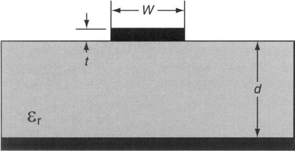
Note that any trace on a printed circuit board can be viewed as a microstrip. In fact, all circuit board traces are microstrips, but only some are designed that way. The complete analysis of a microstrip is a bit complex but a few approximations will help. The first approximation is that the ground plane is finite in size, since it cannot really be infinite, but it must be much larger in all directions than the transmission line. Another approximation concerns the free space above the trace. Most circuit boards are used in an enclosure of some type; if a microstrip is used on the circuit board then any metal cover must be kept far above the traces. This will keep the electric field lines above the microstrip from becoming distorted by the presence of a cover.
These approximations allow one to write a simple formula for the characteristic impedance of the microstrip. This equation is:

where w is the width of the microstrip trace (in mils, which are 0.001 of an inch), d is the distance to the ground plane (again, in mils), t is the thickness of the trace (in mils) and ![]() r is the relative dielectric constant of the dielectric material used in the circuit board. The result is Z0, which is the characteristic impedance of the transmission line in ohms. The term characteristic impedance is simply a way of describing the effects the transmission line will have on the signals it carries. For the purposes of nearly all circuit boards, your goal as a board designer is to produce transmission lines of a known characteristic impedance. This will allow the circuit board to “match” to the components on it, resulting in a minimum of transmission line reflections.
r is the relative dielectric constant of the dielectric material used in the circuit board. The result is Z0, which is the characteristic impedance of the transmission line in ohms. The term characteristic impedance is simply a way of describing the effects the transmission line will have on the signals it carries. For the purposes of nearly all circuit boards, your goal as a board designer is to produce transmission lines of a known characteristic impedance. This will allow the circuit board to “match” to the components on it, resulting in a minimum of transmission line reflections.
What is the dielectric constant (![]() r), you ask? It is a material property of the circuit board you have chosen to use, and it is usually outside of the board designer’s control. Nearly all (99%) of circuit boards are built on “FR-4” woven fiberglass circuit boards, including the ones used in this manual. Exotic high frequency, high power, or low-loss circuit boards are sometimes built on more advanced (and much more expensive) materials. Table 3-2 lists material properties for common circuit board materials. Air is listed for reference only (it’s very hard to build circuit boards in air!).
r), you ask? It is a material property of the circuit board you have chosen to use, and it is usually outside of the board designer’s control. Nearly all (99%) of circuit boards are built on “FR-4” woven fiberglass circuit boards, including the ones used in this manual. Exotic high frequency, high power, or low-loss circuit boards are sometimes built on more advanced (and much more expensive) materials. Table 3-2 lists material properties for common circuit board materials. Air is listed for reference only (it’s very hard to build circuit boards in air!).
Table 3-2
Properties for Circuit Board Materials
| Circuit Board Material | Dielectric Constant | Loss Tangent |
| FR-4 | 4.5 | 0.02 |
| Ceramic (a.k.a. alumina) | 9.8 | 0.0001 |
| Teflon (a.k.a. duriod) | 2.1 | 0.0003 |
| Air | 1 | 0 |
In addition to dielectric constant, the loss tangent is also given for each circuit board type. This is related to the loss an RF signal will experience when it passes through circuit boards made with each dielectric. A lower loss tangent means less loss. Notice how the least expensive material (FR-4) has the highest loss tangent, while the more exotic materials have lower loss tangents.
The process of computing the loss on a transmission line from the loss tangent is even more complex than the computations for characteristic impedance, as it involves the frequency of the signal. Table 3-3 lists a few representative losses of different types of microstrip traces. Notice how the microstrip width is the same for any signal frequency; only the RF loss rate changes with frequency.

You can see that the RF loss of FR-4 greatly increases at signal frequencies above 1000 MHz. The advanced materials are used exclusively for these high frequencies.
The RF loss rate is specified in units of decibels per inch (dB/inch). To compute the actual loss of a stripline, multiply the loss rate by the length of the microstrip. While these losses may seem small, remember that a total loss of only 3 decibels (dB) means that half an RF signal’s power is lost in the microstrip, and only the remaining half may be delivered to the load.
Once you have determined what board material and dielectric thickness you are going to use, it is time to compute the microstrip line width to use to design a microstrip of a given characteristic impedance. The impedance you are shooting for will nearly always be 50OΩ this has become the industry standard for RF controlled impedance circuitry. The only significant exception would be for cable television (CATV) designs, which are typically 75Ω. If you re-arrange the formula given above to solve for the microstrip line width, you get:
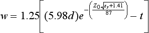
where w is the microstrip width (in mils), d is the dielectric thickness (in mils), t is the trace thickness (in mils), ![]() r. is the dielectric constant, and Z0 is the desired characteristic impedance. Table 3-4 lists microstrip line widths for the most common applications likely to be used. Note that a few mils of error on your board will not dramatically shift the impedance; a ten percent tolerance on characteristic impedance is usually “close enough.”
r. is the dielectric constant, and Z0 is the desired characteristic impedance. Table 3-4 lists microstrip line widths for the most common applications likely to be used. Note that a few mils of error on your board will not dramatically shift the impedance; a ten percent tolerance on characteristic impedance is usually “close enough.”

There are a few last details to discuss about microstrips. In addition to the approximations discussed above (infinite ground and nothing above the line), there are two design guidelines to keep in mind. The first is to keep other traces, either on the same or other layers, as far from the microstrip as possible. A good rule of thumb is to keep all other traces and vias at least five line widths from the microstrip. This will not always be possible, but it is a good goal. Another design guideline is to try to make all of your RF traces into microstrips. This can be as easy as setting your default routing width to your desired microstrip width. In this way, every RF trace you route (no matter how short) will automatically have the proper impedance.
Note that all of the transmission line calculations and tables given in this manual are approximations. When you have an RF circuit board manufactured professionally, be sure to ask for and follow the recommendations of the fabrication house. They should be able to provide you with recommended microstrip width and dielectric thickness for transmission lines of a given characteristic impedance. These recommendations will take into account all of the details of their fabrication process, and should almost always result in properly designed transmission lines. Note also that you, as the board designer, can request the fabrication house to test the impedance of their boards. These tests are usually performed with a TDR (time-domain reflectometer), an instrument which measures reflections on transmission lines. The usual procedure is that the fabrication house will design a test coupon that is built along with your circuit board. The test coupon will allow the fabrication house to quickly and easily measure the characteristic impedance of the microstrips on your board.
Special RF Routing Techniques: Stripline
Stripline is another type of transmission line that can be easily built on a circuit board. It is identical to microstrip, but with ground planes both above and below the trace. Figure 3-7 shows a cross-sectional diagram of stripline. Stripline offers much improved isolation over microstrip, but at the cost of increased RF loss. Striplines are most often used for either high- or low-level RF signals requiring isolation from surrounding circuitry.

As with microstrip, several simplifying approximations allow one to write a simple formula for the characteristic impedance of the stripline. This equation is:

where w is the width of the stripline trace (in mils, which are 0.001 of an inch), t is the thickness of the trace (in mils), d is the total distance between ground planes (again, in mils), and ![]() r is the dielectric constant of the dielectric material used in the circuit board.
r is the dielectric constant of the dielectric material used in the circuit board.
Once again, this equation can be re-written to solve for the stripline width, given a desired characteristic impedance:

Striplines behave identically to microstrip, but with the added benefit that the RF signal is surrounded top and bottom by ground. The ground planes provide a high degree of isolation, so external signals are less likely to interfere with the RF signal on the stripline. The reverse is also true; RF signals on the stripline will radiate much less energy due to the shielding effect of the ground planes. The downside to stripline is increased RF loss. This is due to the fact that the dielectric (insulating) material is now on both sides of the trace, and tends to absorb more of the RF. Table 3-5 lists stripline widths and decibel loss rates for a few stripline designs.

Table 3-6 lists stripline line widths for the most common applications. As with microstrips, you should discuss your stripline requirement with your fabrication house for the most accurate line width to use for a given characteristic impedance.

Striplines are most easily constructed on the inner layers of multi-layer printed circuit boards. If you are making a multi-layer board, then building a stripline layer is easy. First define two ground layers (one on either side of your stripline layer), and then define your stripline layer in the middle. Remember to set the default routing width on the stripline layer to the stripline’s design width. You will have to use vias or through-hole device pins to connect to and from the stripline layer.
Note that the stripline layer can also be used to route other (non-stripline) signals. Just remember to keep all signals far from the striplines. In fact, it is best to place copper (ground) areas around your striplines, right on the stripline layer. This will enclose the RF trace in ground on all sides, and will provide the highest degree of isolation available. The resultant stripline trace is very similar to a coaxial cable, with the signal in the center, completely surrounded by ground. Remember when placing the ground areas to keep them at least five line widths away from the stripline. Use plated-through vias to “tie” the ground areas to the ground planes above and below the stripline layer. Figure 3-8 shows an example stripline layer with ground isolation around each stripline. Notice in the figure how the RF striplines are completely protected by ground areas which are kept far from the stripline trace. Also note that there are other ground areas which are around non-RF traces. These ground areas are allowed to come much closer to the traces, because they are not controlled impedance transmission lines. The circles represent vias, in which signals are crossing through this layer from other layers.

Just because you are building your own two-layer circuit boards does not mean that you cannot use striplines. Simply etch the stripline onto one side of a board, with a ground plane on the other side. Then use another single-sided board (of the same thickness) as the ground plane for the other side of the stripline. Place the two boards together, with the stripline traces touching the empty (non-copper) side of the single-sided board. Drill many holes through the boards in the ground areas (don’t drill through your striplines!), and then use press-in vias or small wires to solder the two ground planes together. Finally, wrap copper tape around the outer edges of the circuit board and solder the tape to both ground planes. Now you’ve made your own stripline circuit board!