Chapter 2
Fabrication Approaches for Conducting Polymer Devices
Dimitrios A. Koutsouras1, Eloïse Bihar1,2,3, Jessamyn A. Fairfield4, Mohamed Saadaoui3 and George G. Malliaras1
1Ecole Nationale Supérieure des Mines, CMP-EMSE, MOC, Department of Bioelectronics, 880, route de Mimet - F-13541 Gardanne, France
2Microvitae Technologies, Hôtel Technologique, Europarc Sainte Victoire, Route de Valbrillant, Meyreuil, 13590, France
3Ecole Nationale Supérieure des Mines, CMP-EMSE, MOC, Department of Flexible Electronics, 880, route de Mimet – F-13541 Gardanne, France
4National University of Ireland Galway, School of Physics, University Road, Galway, H91 CF50, Ireland
2.1 Introduction
During the past decades the field of organic electronics has attracted increasing attention of the scientific community in an attempt to complement traditional silicon electronics and to broaden their horizons [1]. There are a number of good reasons justifying this trend as organic materials present a unique set of properties. In particular, they allow fabrication of thin, flexible, lightweight, environmentally friendly, and low-cost devices [2]. Moreover, they offer ease of processibility, low-temperature solution-based deposition, and the degree of freedom that comes with their chemically tunable properties [3].
Nevertheless, before this new emerging technology becomes mature enough to influence the electronic industry, the major issue of organic film patterning must be addressed. There is an inextricable link between electronic device performance and electronic material patterning and that is the reason why many different methods have been developed through the past years to optimize the fabrication process. Especially when it comes to organic materials, patterning is a challenging task as the technique of choice should be compatible with their special nature.
Unfortunately, despite its comparative advantages, conventional photolithography lacks compatibility with the vast majority of organic electronic materials. This is due to the fact that solvents used during deposition, development, and removal of photoresists have, in most cases, adverse effect on organic films. As a result, the already existing and well-developed industry of conventional silicon-based electronics can only provide limited tools for organic electronics [4]. Thus, the goal of overcoming those incompatibilities is of great importance as it will allow the use of the accumulated knowledge of an already well-established and commercially successful fabrication approach.
Printing techniques have emerged over the last decades as attractive alternatives to photolithography for the manufacturing of electronic devices. These techniques are compatible with roll-to-roll processes and can operate at high speed. Moreover, they only require a limited number of manufacturing steps. They can produce high volume runs, thereby lowering the costs of fabrication. In the second part of this chapter, we will focus on these technologies. A distinction has been made between contact printing technologies (gravure, flexography, screen printing) and noncontact printing technologies (aerosol jet and inkjet). Printed technologies allow the manufacture of a complete device by printing a wide range of inks from conducting to dielectric inks. These new functional inks have been developed to match the electronic requirements and the constraints of industrial processes. Research is ongoing to achieve high resolution down to the micron scale.
In contrast, other nondestructive patterning techniques employed throughout the past years did not manage to live up to their potential. Vapor deposition through shadow masks, soft and hard imprint lithography, thermal transfer process, and laser-assisted printing were originally introduced as alternative approaches promising a convenient and easy way of device fabrication. Nevertheless, all these techniques suffer from numerous drawbacks. In particular, shadow mask deposition is the technique of choice for small-molecule patterning but lacks high-resolution fabrication. Imprint technology, on the other hand, can offer resolution down to 10 nm but it can be used only with a limited number of materials and device architectures [5]. In addition, all of the above techniques have issues with low resolution, poor scalability to larger areas, lack of registration, and the fact that they tend to require complex and costly processing protocols [6]. These disadvantages render them unable to compete with today’s state-of-the-art fabrication processes.
In this chapter, we introduce novel approaches for conducting polymer device fabrication, with a particular emphasis on high-throughput, cost-effective, and simple fabrication techniques, applicable to polymers and able to reproducibly create organic devices with high yield and efficiency. We focus on polymer-friendly photolithography and a printing patterning technique.
2.2 Photolithography
2.2.1 History
The term photolithography is a compound word made up from the Greek words photo (Φως = light), litho (λίθος = stone), and graphy (γραϕή = writing). As implied by its name, photolithography is the process of transferring (writing) a pattern onto a substrate with the help of light.
There are two main historical landmarks in the development of photolithography. The first is the experiments of the Swiss pastor Jean Senebier (1742–1808) of Geneva with resins, in 1782. Senebier noticed that certain resins become insoluble in a solvent (turpentine) after sunlight exposure. The second pivotal moment comes with the work of Nicéphore Niépce on photography in 1826. Niépce, inspired by Senebier, was the first one to produce an image using the properties of light in Chalon (France). He used bitumen of Judea (a form of asphalt) dissolved in lavender oil, to coat a pewter plate and then he covered it with an etched print on oiled paper. The latter would serve as a mask for the 3 h exposure to sunlight that was to follow. During this time, the exposed parts of the resist became insoluble while the protected ones could easily be removed by a mixture of turpentine and lavender oil corresponding to a photoresist behavior classified later as negative. Nevertheless, the first photolithography pattern transfer took place 5 years later, in 1827, by the Parisian engraver Augustin Francois Lemaître. Lemaître used a strong acid to etch a Niépce plate and to create a copy of a gravure of Cardinal d’Amboise, employing for the first time both photolithography and the chemical etching technique in pattern transfer [7, 8].
Photolithography gradually became popular among the members of the scientific community as many of them started to realize the potential of the new technique. A little more than 100 years later, William Shockley and his coworkers at Bell Laboratories wanted to use photolithography for the fabrication of the first integrated circuit. However, the need for a photoresist that could withstand the hydrofluoric etching of silicon dioxide (an important feature for their microfabrication process) made them turn to Kenneth Mees, Director of the Eastman Kodak Laboratories at Rochester New York. Mees contacted Louis Minsk, who in 1935 developed the first synthetic photopolymer known as poly(vinyl cinnamate), the basis of the first negative photoresist. His idea relied on the photoresist becoming less soluble upon exposure to light. Minsk used that feature in order to define which part of the photoresist would dissolve and which would remain on the substrate. In his approach the dissolved parts would be the ones to create the desired pattern. Five years later, in 1940, Oskar Süß developed a positive photoresist (diazonapthoquinone-DNQ) [8], which worked in the opposite way with the pattern formed by the part of the photoresist that remains after exposure to light.
Today, many more chemical substances have been synthesized, characterized, and used in photolithography both as negative and positive photoresists. At the same time, optimization and variation of radiation sources in lithography (X-ray lithography, charged particles lithography, etc.) allow the patterning with nanometric resolution. The comparison with the 0.5–1 mm accuracy achieved by Lemaître during the first photolithographic attempt shows the extent of progress [7].
2.2.2 Basic Principles
The basic principle behind photolithography is the use of light in order to alter the solubility of a thin film that is exposed to it. A mask is a stencil, usually made out of chromium, which protects selected parts of the photosensitive material while the uncovered ones undergo changes in their properties (solubility) during the exposure. After immersion into a chemical developer, the parts that became more soluble are dissolved leaving the desired pattern on the film behind. It is obvious that the photosensitive material plays a key role in the success of the process. This material is typically an organic polymer, called photoresist, which can go through a series of photochemical reactions when exposed to light.
It should also be noted that the term photolithography usually refers to the use of ultraviolet light (UV – wavelengths 436 and 365 nm) during patterning. Nevertheless, deep ultraviolet (DUV –wavelengths 248 and 193 nm) and extreme ultraviolet (EUV – wavelengths 5–100 nm) photolithography techniques are both feasible and appealing, as in theory when the wavelength of the light source diminishes the feature resolution increases. Nevertheless, it is difficult to find light sources with enough output power, the proper photoresists, and the optical elements [9] for those short wavelengths. Moving a step further, X-ray lithography, charged particle lithography, or atomic force microscopy (AFM) lithography promise even better resolution, posing at the same time extra technological challenges. In this chapter every time we use the term photolithography it will be implied that we refer to UV photolithography.
Returning to photoresists, they can roughly be divided into two categories: positive photoresists (positive tone) and negative ones (negative tone). A positive photoresist is a photoresist, which, when exposed to light, changes chemically and/or structurally becoming more soluble to an organic developer while, ideally, it was insoluble before. The mechanism behind this transformation can be either a polymer chain scission (e.g., poly(methylmethacrylate) (PMMA) photoresist) or a photo-induced change in the polarity of the molecule (e.g., two component DNQ-phenolic novolac resin) [7, 10]. A negative photoresist works in exactly the opposite way. The photoresist is soluble to the developer and exposure to UV light either promotes polymeric cross-linking or starts the polymerization of the monomers. That renders the exposed photoresist insoluble to the developer, and hence unexposed parts of the film are removed during the development step that follows. Common negative tone photoresists are the bis(aryl) azide rubber resists and the Kodak Thin Film Resist (KTFR) (an azide-sensitized poly(isoprene) rubber) [7, 10].
For both these types of photoresists the exposure, the development, and the final pattern formation on the substrate are depicted in Figure 2.1.
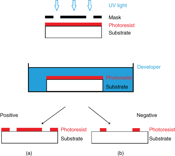
Figure 2.1 Pattern transfer for a positive (a) and a negative (b) photoresist.
In general, positive photoresists are more expensive than negative ones but can offer higher resolution. This feature, along with the fact that positive photoresists can be developed in less toxic water-based developers, made them more popular than their negative counterparts in industry. Nevertheless, many steps forward have been made lately in the synthesis and development of negative resists. As a result, the newer negative tone resists are water developable and can also offer high resolution [7]. In addition, negative photoresists traditionally adhere better to substrates and they are more resistant to wet or dry etching than positive ones [7]. In conclusion, the choice of a proper photoresist depends on many different parameters (cost, resolution, pattern geometry, etc.), all of which need to be taken into account before a decision is made.
Currently, photolithography is the most popular technique of patterning in the integrated circuits industry. It offers a reliable and reproducible way of building electronic devices with great accuracy and high resolution. Its main disadvantage is the limitations in the topography, as it can only be implemented on planar substrates. The process performance can be evaluated through three figures of merit:
- Resolution: A measure of the minimum size of a feature that can be patterned. It needs to be as high as possible in order for the feature size to be small.
- Registration: A measure of how accurately patterns on different layers can be aligned with respect to each other.
- Throughput: The number of substrates that can be exposed per hour. The higher the throughput the more efficient the process.
2.2.3 Fabrication Steps
The typical fabrication steps that take place during microfabrication are briefly reviewed below.
2.2.3.1 Substrate Cleaning
The first and definitely one of the most important steps in device fabrication is substrate cleaning. Several different types of substrates can be used for electronic circuit development. Silicon wafers are very common, especially in silicon-based semiconductor industry, but other kinds of substrates may also be employed. Glass slides, conformable substrates (like Parylene-C), or even less conventional substrates such as textiles and silk are among them. Despite the fact that some of those substrates may have special requirements or even incompatibilities with the standard cleaning protocols, the cleaning step cannot be easily omitted. Keeping the substrate free of contaminants is a matter of great importance as the degree of its cleanness affects the quality of the deposited film. Moreover, particles on the substrate could potentially lead to damage of the photomask during contact photolithography exposure or even cause, in some cases, undesirable masking effects due to light diffraction. Among the contaminants that should be removed before coating the substrate with photoresist are atmospheric dust from operators and equipment, organic particles, moisture, H2O residue films, solvent stains, smoke particles, residual resist, particulates, and chunks of granular matter [7, 11].
The cleanliness of the fabrication environment is of critical importance; hence, all fabrication steps take place in a clean room environment (typically class 100) that allows the presence of up to 100 particles (sized 0.5 µm or larger) per cubic foot of atmosphere. An environment such as this minimizes the amount of unwanted particles in the milieu and as a result it minimizes the number of unwanted contaminants on the device as well. Taking this environment as granted, typical cleaning procedures may include both wet and dry methods. Sonication in water soap baths or solvent baths is normally employed for the removal of particles (both inorganic and organic). In some cases piranha solution (a 3 : 1 mixture of sulfuric acid and hydrogen peroxide) can also be used to detach organic particles from the substrate. Additional approaches include thermal treatment at high temperature (dehydration bake), plasma cleaning, vapor cleaning, and supercritical cleaning with CO2 during which supercritical fluid of carbon dioxide is used for removal of inorganic and organic contaminants from cracks and clefts owing to its ability to penetrate into crevices [7, 11].
2.2.3.2 Deposition of the Photoresist
Once substrate cleanness is ensured, deposition of the photoresist on the substrate follows. Among the ways of depositing polymers on a substrate spin-coating is the one that can guarantee uniformity, reproducibility, and precision during deposition. It is a well-known, traditional technique that is easy to use and offers control of the film thickness. The main drawback is the fact that the majority of the processed material is wasted.
Consequently, spin-coating deposition has been the method of choice for photoresist thin-film formation during fabrication for several decades now. During this approach, a small droplet of the photoresist is placed in the middle of the substrate, which is secured on a chuck via vacuum. Centripetal acceleration spreads the photoresist on the substrate. Although almost 98% of the initial material is spun off, eventually a thin film of photoresist is deposited on the substrate, as shown in Figure 2.2.
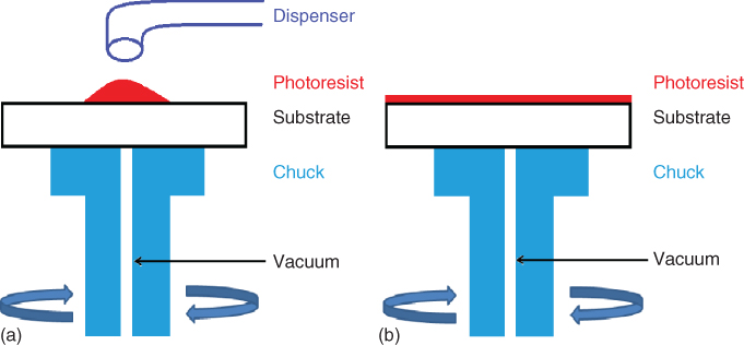
Figure 2.2 (a) Photoresist is placed on the substrate. (b) Film formation due to centripetal acceleration.
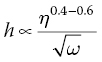
Thickness h of the photoresist is controlled through specific parameters of the process. The angular spinning speed ω and time t as well as the liquid density ρ, material viscosity η, and evaporation rate ee are the most important factors affecting the film’s formation. During this process, complex nonequilibrium phenomena take place, and it is believed that two parts contribute to the rate by which the thickness of the film changes over time: a part that refers to the effect of the angular spinning speed and a part connected to the evaporation rate of the photoresist ee. Generally, the spinning cycle can be separated into two stages: a very fast coating stage (when the photoresist is spread on the substrate) and a longer drying stage (during which the solvent evaporates). In any case, the rheology behind the film formation is complex, especially if the evaporation of the photoresist is taken into account. Therefore, the film thickness is usually given by the empirical expression (2.1) [7, 11, 12]
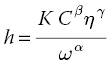
where K is an overall calibration constant, C is the polymer concentration in g/100 ml, and η is the solution’s viscosity. The exponential parameters α, β, and γ are determined experimentally. Once these parameters are set, a calibration curve is obtained that can provide the film thickness for a given polymer and solvent. Usually, film thickness is inversely proportional to the square root of the angular spinning speed ω and proportional to the solutions viscosity η to the 0.4–0.6 power [12].
There are two common ways to realize the photoresist’s dispersion on the substrate: the static dispense and the dynamic dispense. During static dispense a drop of photoresist is deposited on the substrate near its center while it is stationary. The amount of material deposited is in direct correlation with the viscosity of the photoresist (more viscous photoresists require more material to be placed) and the size of the substrate (bigger substrates require more material to ensure the total coverage of the substrate). On the other hand, dynamic dispersion dictates an initial step of spinning at a low speed (typically 500 rpm) while the dispensing takes place. After that, the substrate is accelerated to its final speed. Theoretically, this approach facilitates the wetting of the substrate and consequently the spreading of the material, leading to less waste.
For both approaches, the angular spinning speed and the time of the spinning are the two parameters that affect the final thickness of the film. In general, high speed and longer spinning times lead to thinner film formation.
2.2.3.3 Post-apply Bake
What follows is a thermal treatment step called post-apply bake (PAB) (or soft bake). It usually lasts for a minute or two on a hot plate at 110 °C. The purpose of this step is to evaporate the remaining solvent from the photoresist and to densify it just before exposure. This renders the coated film more stable and reduces the probability of the covered substrate to stick to the mask during exposure.
2.2.3.4 Use of the Mask/Alignment/Exposure
Exposure stands at the very heart of the fabrication process. The basic principle behind photolithography, after all, is altering a photoresist’s solubility by delivering energy to it via radiation. The stencil that is used to transfer the desired pattern on the photosensitive film is called the mask. Generally, a mask is made of glass (transparent to UV radiation) with a metal pattern on it (usually a 800 Å chromium film is used). The glass windows allow the radiation to pass through it with very little absorption while the metal pattern protects the underlying photoresist from any interaction with light. Masks are constructed with electron beam lithography, which can result in higher resolution than photolithography [7]. Special care is also taken in the proper alignment of different device layers to each other during the exposure. As previously stated this is one of photolithography’s figures of merit (Registration) and is handled with the use of special marks (alignment marks) strategically placed on the different layers [9]. After all, registration is one of the main advantages of photolithography compared to the rest of the techniques, along with high throughput due to its parallel nature.
There are three different ways to perform the exposure: contact, proximity, and projection mode, as shown in Figure 2.3.
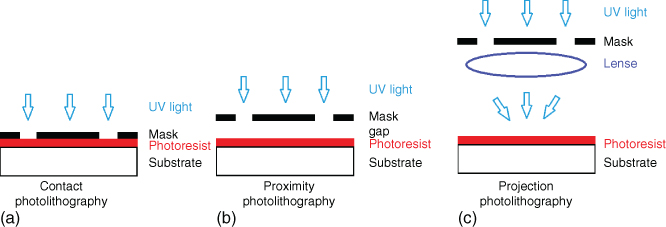
Figure 2.3 Schematic representation of the three exposing modes. (a) Contact photolithography, (b) proximity photolithography, and (c) projection mode.
2.2.3.4.1 Contact Mode
Contact mode lithography was the first mode to be used in the early 1960s. In this approach the substrate is in physical contact with the mask during the exposure. The alignment of the substrate is performed with the creation of a temporary spatial gap between the two. The resolution of contact printing is rather high as it can go down to the wavelength of the radiation used. Nevertheless, the high risk of mask damage due to the contact with the substrate motivated a search for alternative modes of photolithography.
2.2.3.4.2 Proximity Mode
Here, the mask and the substrate are not in contact as there is a small gap (10–50 µm) maintained between the two. That protects the mask from damage but at the same time lowers resolution due to diffraction effects.
Contact and proximity mode printing are known together as shadow printing. The resolution r for them is given by the formula [9, 11, 12]
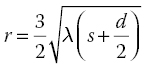
where λ is the radiation wavelength, s is the distance between the mask and the substrate, and d is the photoresist thickness.
2.2.3.4.3 Projection Mode
This is the mode of choice used in semiconductor industry from the mid-1970s to date. In projection printing, there is no direct contact between the mask and the substrate as the mask is projected onto the substrate through a lens system. This approach protects the mask from damage since there is no physical contact involved, as shown in Figure 2.3. In addition, the demagnification of the mask pattern achieved with the optics results in high resolution and makes the mask fabrication a little easier [7].
The resolution r for projection printing is given by [9, 11, 12]

where k is a coefficient that depends on process-related factors and NA is the numerical aperture.
2.2.3.5 Development
After exposure, a development step will allow the latent resist pattern formed to be revealed. Selective dissolution of the resist creates a relief that will serve as a mold for the next fabrication steps. Development is of extreme importance as it controls the quality of the transferred motif.
There are two main approaches to performing this step: wet development and dry development.
2.2.3.5.1 Wet Development
In wet development, aqueous and organic solvents are used to selectively dissolve the exposed photoresist. Positive photoresists are developed in aqueous alkaline solutions while negative photoresists are developed in organic solutions. Aqueous development is preferable for environmental reasons and that is why newer negative resists may also be developed in aqueous solutions [7]. The aqueous solutions are usually tetramethyl ammonium hydroxide (TMAH) based. The solvent is applied either by immersion or by spraying (with or without substrate spinning) [7, 12].
2.2.3.5.2 Dry Development
Dry development is an alternative approach dictated mostly by the need for developing cleaner fabrication techniques. It is based on oxygen-reactive etching for the appearance of the desired pattern. Exposure alters the photoresist’s etching resistance rather than its solubility [7, 12]. After development, the substrate is rinsed and dried with dry air or nitrogen. Visual inspection guarantees the quality of the pattern and the lack of defects.
2.2.3.6 Descumming and Post-baking
Descumming is a mild oxygen plasma treatment to remove any residual resist after development. It removes tiny amounts of unwanted material without harming the desired features. Patterned resist is also affected, but as long as only a few hundred angstroms are removed this does not cause any fabrication concerns.
Just before the pattern printed in the photoresist is transferred onto the substrate, a post-baking step (also known as hard baking) takes place. Hard baking promotes interfacial adhesion of the film and removes the residual solvent. It usually occurs at the temperature of 120 °C (slightly higher than the temperature used for soft baking), which additionally cross-links the photoresist, making it harder and more resistant to the etching steps that follow. Special care should be taken in order for the temperature not to cause flow or melting of the photoresist as this will degrade the profile of the resist.
2.2.3.7 Pattern Transfer
The previous steps create the desired pattern on the photoresist. The next goal is to transfer this pattern (or its negative) from the photoresist onto the substrate. There are two different methods to achieve this goal: a subtractive process and an additive one [4, 12].
In the subtractive method, first a material film is deposited on the substrate. Photolithography creates a positive image of the pattern and then etching removes the excess material, leaving behind the desired structure. The additive method, on the other hand, uses photolithography to create first a negative image of the pattern and then to realize its positive version via selective deposition of material. Both these methods will be further developed with case studies later in this chapter.
Etching is one of the most crucial parts in fabrication. Selective etching creates the required polymer microstructure during the subtractive approach, while it controls the material deposition in the additive one. In general, etching is a method of removing material that is not protected under the photoresist. It can be done chemically, mechanically, or with a combination of the two mechanisms.
Wet etching was initially the method of choice in the microelectronic industry. An acidic solution was used to erode the thin film not covered by the photoresist, creating a selective 3D structure. However, the method’s isotropic nature usually resulted in an undercut profile damaging the overall resolution. Consequently, new dry etching approaches quickly became popular as they could provide etching in an anisotropic way. Plasma etching, in particular, uses plasma (an ionized gas) to anisotropically and selectively etch only the patterned material and not the photoresist above it, allowing fabrication with sub-micrometer resolution. As dry techniques are easily automated and remove the need for toxic developers, it is not a surprise they quickly rose to dominance [11].
Many different dry etching techniques have been developed, but among them reactive ion etching (RIE) offers the benefits of both the chemical and the physical etching worlds. RIE uses plasma to create ionized atoms that can be accelerated by an electrical field and cause a directional sputtering of the substrate. This is extremely important in giving anisotropy to the technique. The charged molecules gain kinetic energy, which they transfer to the film in the collision, etching it vertically. At the same time they provide the energy for an etching reaction to take place, which is selective due to its chemical nature.
The deposition of the material of interest mentioned above is done with a number of different techniques. Chemical vapor deposition (CVD), physical vapor deposition (PVD), sputtering, and electroplating are among them. Here, we will focus on thermal evaporation as it is widely used for metal film deposition and it will prove to be extremely useful for the fabrication of organic devices that follows.
2.2.3.8 Stripping
The last step of the fabrication process is the removal of the remaining photoresist. That will create patterns by selectively discarding the evaporated material that was deposited on the photoresist while leaving the rest intact. The photoresist acts now as a sacrificial layer and is removed along with the metal layer on top of it, creating the desired metal profile. Photoresist stripping is usually performed with the help of organic solvents. Acetone is very commonly used for this task, along with other phenol-based commercial strippers. Nevertheless, environmental issues favor the use of dry stripping methods such as oxygen plasma. In any case, the ultimate criterion in the stripping approach is not to destroy the target material film. Especially for organic materials, this criterion poses a number of extra difficulties due to incompatibilities with the majority of solvents.
2.2.4 Photolithography in Polymer Device Fabrication
The previously presented steps of conventional photolithography could have theoretically been implemented in polymer device fabrication as well. The main challenge of organics, though, is the incompatibility issues between organic films and the solvents used during optical lithography. Unfortunately, the solvents employed for depositing, developing, and removing photoresists usually have a destructive effect on organic materials (including dissolution, cracking, swelling, and delamination of the polymer film [4]). Two different but representative strategies have been developed during recent years to overcome these limitations, and are presented here.
2.2.4.1 Sacrificial Layer Method
An alternative way of patterning organic materials, developed by DeFranco and coworkers, is based on the use of a poly(monochloro-p-xylylane (Parylene-C) sacrificial buffering layer [4]. Parylene-C (a polymer widely used as a barrier layer) is employed to protect the organic film during each step of the photolithography fabrication (deposition, development, and strip of the photoresist). After Parylene-C deposition, the formed film is inert and resistant enough to withstand a photolithography step on it.
From this point, two different fabrication methods (an additive and a subtractive one) lead, eventually, to the organic material patterning [4, 13, 14]. For the subtractive method the developed photoresist serves as a mask to selectively etch and remove both the Parylene-C layer and the organic film under it. In the additive method, on the other hand, the photoresist acts as contact mask and an etching step leaves behind voids in the Parylene-C to be filled with the polymer. Both these approaches can give high-quality patterned polymer films, and are shown schematically in Figure 2.4.
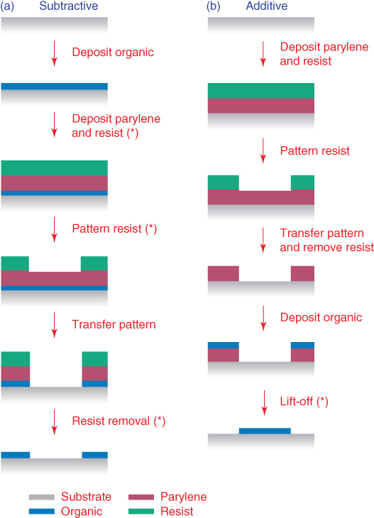
Figure 2.4 (a) Subtractive and (b) additive fabrication approaches. The asterisks indicate the steps where the organics would be damaged during conventional photolithography.
(DeFranco et al. 2006 [4], Reproduced with permission of Elsevier.)
The next two case studies are paradigms of the aforesaid additive and subtractive methods implemented in organic device fabrication. The active area of those devices is covered with a thin poly(3,4-ethylenedioxythiophene) doped with poly(styrene sulfonate) (PEDOT:PSS) polymer film while the electrodes and their wiring are gold patterned with the use of conventional photolithography techniques. Both methods are versatile, generic, and can be used for direct patterning of polymer films in a variety of organic devices (polymer-covered electrodes, organic transistors, etc.).
2.2.4.1.1 Subtractive Patterning
A subtractive method that can result in high performing devices was presented in 2011 by Khodagholy and coworkers [15]. In this approach, PEDOT:PSS-covered gold electrodes were fabricated on a 2 µm Parylene-C film that served as a flexible substrate. Initially, gold electrodes, interconnections, and pads were patterned on a Parylene-C film via standard photolithography. A second 2 µm thick film of Parylene-C was used to insulate the device while a second photolithography step followed by oxygen etching (RIE) opened windows over the recording sites and pads. The polymer (PEDOT:PSS) was deposited through spin casting and the devices were coated with a third (sacrificial) layer of Parylene-C. The final photolithography and etching step defined the PEDOT:PSS-coated electrodes. Immersion of the device in deionized water promoted the removal of the Parylene-C sacrificial layer exposing the electrodes (Figure 2.5).
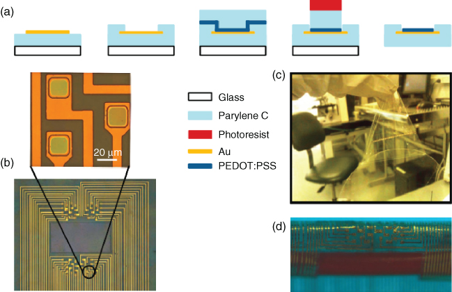
Figure 2.5 (a) The main steps of the fabrication process. The final array of electrodes is mounted on a Parylene-C substrate. (b) Optical image of the electrode array with a close-up on three electrodes. (c) The electrode array can support the weight of a quartz wafer. (d) The array can conform to a cylinder of 2.2 mm radius.
(Chang et al. 2007 [16]. Reproduced with permission of American Chemical Society.)
The success of the process relies on the fact that the polymer film adheres better to gold than to the Parylene-C film above it. In addition, due to its hydrophobic character, deionized water facilitates the sacrificial layer’s peeling off without affecting the quality and conductivity of the organic film. The conducting film’s integrity is also maintained during the Parylene-C deposition process. The above points render the method generic, versatile, and usable for different types of conducting polymers as they also become hydrophilic when doped.
Parylene-C plays a key role in the fabrication approach studied. It not only protects the organic film, which is sensitive to solvents, but also offers electrical insulation for the device, which is imperative for its functionality. Parylene-C is a member of the greater poly p-xylylene family and is produced with the substitution of Cl on the aromatic ring (Figure 2.6).

Figure 2.6 Chemical structure of (a) poly(p-xylylene) and (b) (chloro-p-xylylene).
It has been extensively used in the past for coating purposes. It is a green chemistry polymer as it is chemically inert [16] and needs no initiator for solvent-free deposition as a coating film [17]. Hence it can be easily deposited on and removed from the polymer films without causing their chemical deterioration [15].
The material is deposited from its vapor phase via a CVD method proposed by Gorham. Its dimer is heated at 150 °C (P = 1 Torr) creating the vapor phase of the material. A pyrolysis stage follows at 680 °C (P = 0.5 Torr) that cracks the dimers to give birth to monomer units. The final polymerization step takes place on the device substrate at 25 °C (P = 0.5 Torr) resulting in the formation of a thin polymer film [17]. Most importantly, coating thickness can be controlled accurately and reproducibly through the amount of dimer used.
2.2.4.1.2 Additive Patterning
An additive method of polymer patterning was presented by Sessolo and coworkers in 2013 [3]. Once more, gold electrodes, contact pads, and their interconnections were patterned lithographically on a glass substrate. The device was coated with a 2 µm Parylene-C film that adhered on the substrate with the use of 3-(trimethoxysilyl)propyl methacrylate (−174 Silane). A soap solution was spin cast on Parylene-C to act as an antiadhesive layer between the first and a second 2 µm Parylene-C (sacrificial) film. Photolithography and an etching step were then used to open windows above the electrodes and the pads. After that, the polymer (PEDOT:PSS) was deposit by spin coating on the device, and a final peel-off step defined the final polymer device structure, shown in Figure 2.7.

Figure 2.7 (a) The main steps of the fabrication process. The gold electrodes were first patterned lithographically and then Parylene-C was used for the device insulation. A second photolithography step followed by an etching step defines the well for the PEDOT:PSS deposition that follows. A mechanical peel off concludes the fabrication. (b) A microelectrode array device fabricated on a glass slide; (c) a close-up of the PEDOT:PSS covered electrodes (scale bar 50 µm).
(Sessolo et al. 2013 [3]. Reproduced with permission of John Wiley and Sons.)
Once again, the method is generic and versatile, and it can be adapted according to the desired device geometry. Moreover, different conducting polymers can be used as active layers as long as they can be deposited from solution.
2.2.4.2 Orthogonal Photoresist Method
A different way of dealing with the polymer patterning challenge comes with the utilization of orthogonal solvents. The term orthogonal refers to solvents in which the organic compounds are insoluble, a feature that allows not only the patterning of organic electronic materials but also their multilayer deposition.
Hydrofluoroethers (HFEs) in particular belong to a class of solvents, which, besides being nontoxic and environment friendly, are also orthogonal to many organic materials [18]. Consequently, they are ideal candidates for polymer patterning as long as a photoresist compatible with them is synthesized.
A photoresist such as this was presented in 2009 by Taylor et al. [5]. The HFE compatible material is a copolymer composed of a highly fluorinated monomer 1 (3.3.4.4.5.5.6.6.7.7.8.8.9.9.10.10.10-hepta-decafluorodecyl methacrylate) and a photosensitive monomer 2 (2-nitro-benzyl methacrylate) (Figure 2.8). Its solubility in HFE solvents can be modified after UV exposure due to structural changes to the photosensitive 2 part of the molecule, resulting in a negative tone photoresist. In addition, it is acid stable, a feature extremely useful when it is used to pattern acidic polymers.
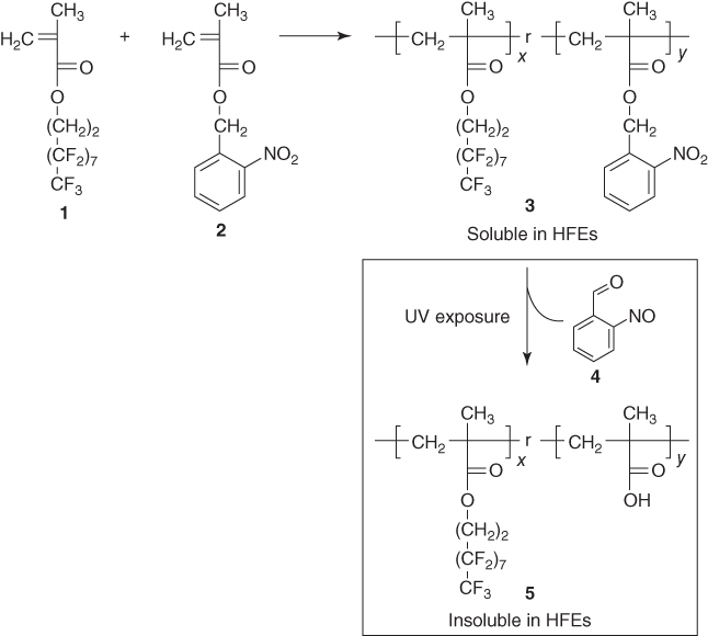
Figure 2.8 Synthesis of the HFE-soluble photosensitive copolymer 3. Exposure to UV light renders the polymer insoluble in HFEs.
(Taylor et al. 2009 [5]. Reproduced with permission of John Wiley and Sons.)
As a proof of concept, a bottom-contact organic thin-field transistor was fabricated with a pentacene channel and PEDOT:PSS drain and source electrode by the same group. On a Si wafer, a 360 nm oxide was grown thermally just before PEDOT:PSS was spin cast and baked at 180 °C for 10 min. Photoresist 3 was then spun on the PEDOT:PSS layer and patterned lithographically with HFE-7200 (an isomeric mixture of methyl nonafluorobutyl ether and methyl nonafluoroisobutyl ether) acting as its developer. The image was transferred on the PEDOT:PSS with oxygen etching and the remaining photoresist was lifted off in a propan-2-ol (10% by volume)/HFE-7100 mixture. Photoresist 3 was spun again on the patterned PEDOT:PSS film, this time followed by UV light exposure and a development step. Pentacene was thermally evaporated, and removal of the photoresist by the previously used solvent mixture defined a pentacene channel connecting the PEDOT:PSS source and drain electrodes (Figure 2.9).

Figure 2.9 Main fabrication steps of the PEDOT:PSS/pentacene bottom-contact organic thin-film transistor. PEDOT:PSS was first spin cast on the substrate and patterned photolithographically with the use of the photoresist 3 as a developer and a following oxygen etching step. The process was repeated for the deposition of the pentacene film giving birth to the organic thin-film transistor.
(Taylor et al. 2009 [5]. Reproduced with permission of John Wiley and Sons.)
In a similar approach, Hwang and coworkers were able to pattern polymer materials using supercritical carbon dioxide (scCO2) as the solvent [19] to fabricate an organic light-emitting diode (OLED). ScCO2 is an environment-friendly fluid used in the dry photolithography process (DPP) for resist stripping owing to its physical and chemical advantages. Most importantly, it is a poor solvent for most ionic, high molecular weight, and low pressure organic materials.
In their work, a light-emitting polymer (LEP) was patterned on top of a PEDOT:PSS active layer. PEDOT:PSS was first spin cast on glass coated with indium tin oxide (ITO). A negative tone copolymer was synthesized from 1H,1H,2H,2H-perfluorodecyl methacrylate (FDMA) and tert-butyl methacrylate (TBMA) and deposited on the PEDOT:PSS layer. After UV exposure, scCO2 was used for the development followed by oxygen plasma cleaning treatment and an LEP spin-casting step. A thermally deposited CsF(1 nm)/Al(40 nm) film completed the ITO/PEDOT:PSS/LEP/CsF/Al structure (Figure 2.10).
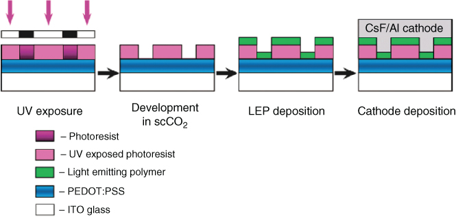
Figure 2.10 The main steps of the OLED fabrication process. PEDOT:PSS was spun on the substrate and a negative tone photoresist was used to pattern the LEP on top of PEDOT:PSS. The developer used was scCO2, which is not harmful to the active material. A CsF(1 nm)/Al(40 nm) film completes the device fabrication [20].
(Glowacki 2015, http://pubs.rsc.org/en/Content/ArticleLanding/2015/TC/c5tc00556f#!divAbstract. Used under CC-BY-3.0 http://creativecommons.org/licenses/by/3.0/.)
2.3 Printing
The term printed electronics comes from bridging the fields of both printing and electronics; this union of two fields allows for simpler methodology to fabricate inexpensive electronic components. The market for printed electronics has been estimated around 57 billion dollars (US) in 2019 by IDTechEx [20], and there are significant opportunities for companies to enter this market. The advantages of printing techniques include direct ink transfer to substrates and a reduction in the number of manufacturing steps. Furthermore, motivations for the continued use of printing arise from its flexibility, high processing speeds, ease of customization, reduction in manufacturing costs, the possibility of printing on inexpensive flexible plastic or paper substrates, and the ability to print with different types of materials.
Recently, there has been a growing interest to adapt classical printing techniques to be able to print new functional materials, especially with electronic inks for device fabrication. This idea has the potential to open up new markets and opportunities for both industry and academia. By exchanging traditional graphic inks for electrically functional inks, one can directly print or fabricate interconnections, antennas, sensors, and so on. By using printing techniques, one can avoid the large number of processing steps (lithography, etching, etc.) used in conventional electronic fabrication techniques.
Technologies such as screen printing or inkjet are promising technologies, and have been extensively studied over the last few decades. They are envisaged to replace traditional manufacturing technologies, such as lithography, to fabricate new electronic components. In this part, we will describe the different printing techniques with an emphasis on conducting materials. We will separate the topic into two categories: contact and noncontact printing.
2.3.1 Contact Printing Technologies
2.3.1.1 Gravure
Gravure printing is a process coming from intaglio developed in the nineteenth century. It uses a rotary printing press and operates at high speed processing (up to 100 m min−1). It is adapted for large volume runs such as books or magazines. Gravure is based on the direct transfer of the ink to the substrate from an engraved cylinder to the substrate (Figure 2.11). This cylinder is electroplated, for instance, with copper, and engraved electromechanically or by laser to create microcells. A chromium zinc layer is generally added to protect the cylinder. The volume of the ink that is deposited is determined by the geometry of the microcells. Then, the ink is transferred by capillary force from the microcells to the substrate when pressure is applied between the gravure cylinder and the substrate. Moreover, a doctor blade station is used in order to remove any excess ink and to ensure good film uniformity. Gravure allows designs with high resolution up to 20 µm and presents good printing quality and process reproducibility. It is compatible with a wide range of solvents or water-based inks. The required viscosity of the inks is comprised between 10 and 500 cP. Nevertheless, this process exhibits some limitations in terms of maintenance and cost of manufacturing mainly because of the price and the weight of cylinders.
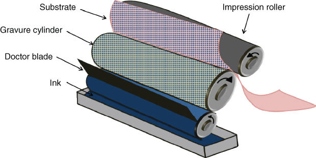
Figure 2.11 Gravure process.
This technique has been studied for electronic applications such as for the realization of field-effect transistors (FETs) or photovoltaic cells [21]. A few groups tested the printability of conducting polymers to print functional multilayers to fabricate FETs [22] or to realize solar cells with laboratory gravure modules [23–25]. Gravure-printed PEDOT:PSS electrodes demonstrated high mechanical flexibility and stretchability in comparison with conventional indium tin oxide (ITO) on flexible substrates. For instance, Hübler et al. fabricated photovoltaic cells by printing PEDOT:PSS as the anode and a poly(3-hexylthiophene-2,5-diyl):[6,6]-phenyl-C 61 butyric acid methyl ester blend (P3HT:PCBM) as the photoactive and hole transport layers on paper [4]. Yang et al. used an industrial gravure printing proofer to process the photovoltaic module, where they print conducting polymers on flexible substrates already coated with ITO [26]. Recently, gravure has been investigated to realize impedance-based electrochemical biosensors [27], which paves the way to fabricate the new generation of flexible devices for biological applications.
2.3.1.2 Flexography
Conventionally, flexography is used for printing food packages and magazines. Flexography is compatible with flexible substrates such as plastics or cardboards. It is a process combining a system of cylinders and a flexible relief plate (Figure 2.12). An engraved anilox roll is used to transfer the ink from the pan. The amount of the ink is fixed by the volume of the microcells’ cylinder. A doctor blade ensures that the thickness of the ink is uniform. Then, the printing of the ink is assured by the contact between the substrate and the plate cylinder. These plates are usually made from rubber or photopolymer materials and produced by photolithography.
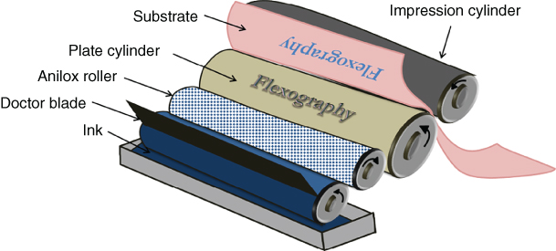
Figure 2.12 Flexography process.
This technology is compatible with a wide variety of inks: UV-cured inks and solvent- or water-based inks with a viscosity ranging from 10 to 100 cP. Resolution up to 50 µm can be reached. The use of the plates lowers the cost of fabrication and allows the printing of large volume runs with high processing speed (up to 180 m min−1). The costs are reduced in comparison with gravure but plates can be degraded with the use of solvents. One of the major undesirable effects of this process is the halo that appears on the edge of the printed pattern. The default comes from the deformation of the plate when the pressure is applied between the plate and the substrate squeezing the ink.
Only few studies chose this approach for printed electronic applications [28, 29]. Hübler et al. [30] use a laboratory flexographic test printing device to print the gate and contact electrodes using conducting polymers to fabricate transistors. Krebs et al. [31] reported using this process to improve the wettability of surface to slot die conducting polymer while Yu et al. [32] printed the silver layer to realize grids to replace ITO in polymer cells.
2.3.1.3 Screen Printing
Screen printing is a simple and versatile technique used in many applications such as textiles or advertisements. It has been originally invented in China, and imported into Europe in the eighteenth century and developed in the second half of the twentieth century. The first patent was published in 1907 by Samuel Simon, and the technique became more popular in the 1960s with artists such as Andy Warhol [33].
Screen printing is a stencil method that uses a mesh stretched over a frame to transfer the ink to the substrate. The ink is pushed into the opening of the mesh through a squeegee (Figure 2.13). The mesh is usually made from nylon, polyester, or a stainless steel. Two different categories of screen printing have been developed and can be integrated for roll-to-roll manufacturing: the flatbed screen or the rotary screen. The flatbed screen (Figure 2.13a) is used in laboratories or in production and the rotary is adapted for large-scale process with a production speed up to 100 m min−1. In this case, the squeegee and the ink are placed in the rotary screen (Figure 2.13b), making the maintenance procedure difficult. The printing resolution can be up to 100 µm and depends on parameters such as the surface energy of the substrate, the ink viscosity, the mesh size, and counts.

Figure 2.13 (a) Flatbed screen printing. (b) Rotary screen printing.
Screen printing is one of the most robust technologies that have been developed in the last few years as it is compatible with a wide range of substrates such as textiles, clothes, papers, and glass. This process requires high-viscosity inks (up to 10 000 cP) and the deposited thickness can go up to few hundreds of microns. Screen printing is already used to print interconnections for printed circuit boards and antennas for RFIDs (Radio Frequency IDentifications), active layers [34] and electrodes [35, 36] for solar cells or organic thin-film transistors [37], and emitting layers in OLEDS [38–40] (Figure 2.14). Many studies [41–43] and patents [44–46] have reported the use of screen printing for biosensing applications. They demonstrated the feasibility of such devices to detect bioelements or to fabricate amperometric biosensors.

Figure 2.14 Screen printer using Clevios™ ink.
(Reproduced with permission from Heraeus.)
2.3.2 Noncontact Printing Technologies
Noncontact printing technologies are digital writing approaches and present many advantages because they do not require masks and the geometry can be customized and changed on demand. Also, the ink is digitally delivered to the substrate, thus limiting the wastage of materials and allowing processing of designs at low cost.
2.3.2.1 Aerosol Jet
Aerosol jet printing has been developed since the 2000s and shows a promising future for industrial applications. This technology allows printing a large range of ink viscosities (from 1 to 2500 cP). The principle is based on the ejection of fluids even with nanoparticles from a chamber to the substrate (Figure 2.15), a new technology that uses the atomization of suspension by an ultrasonic or a pneumatic system. The formed droplets are guided by a jet stream up to the printing nozzles. The aerosol printing can produce conformal coating and resolution down to 10 µm with processing speed up to 1.2 m min−1.

Figure 2.15 Aerosol process.
Few studies mention aerosol printing in literature [47, 48]. Recently, it has been evaluated for diverse applications such as solar cells and thin-film transistors. For instance, aerosol jet has been used to print the conducting polymer as an active layer in solar cells [49] and to fabricate electrodes for TFTs [50]. Aerosol has been also studied for the deposition of DNA or enzymatic layers and for the functionalization of electrodes in biological sensors [51].
2.3.2.2 Inkjet
Inkjet is a noncontact technology commonly used for daily use printing applications (home or office). This process can be integrated in industry in roll-to-roll processes in the production line. Advances in these technologies have been seen recently, for instance, the standardization and commercialization of 3D printing and the creation of new functional inks for electronics.
2.3.2.2.1 History
The physics behind inkjet was first described in 1878 by Lord Rayleigh [52], the pioneer in studying the mechanism of the liquid jets’ instability. The first patent was deposited by Elmqvist [53] in 1951 at Siemens-Elema Company.
In the early 1960s, Sweet developed a model [54] in Stanford University, in which he assumed that the trajectory of ejected droplets can be controlled electrostatically through an externally applied electric field. This process has been called continuous inkjet (CIJ) and it is still used for some applications. Later, a drop-on-demand (DOD) technology was proposed in 1972 by Zoltan [55] and Kyser and Sears [56] as an alternative to CIJ. A single droplet is formed and detached by each of the printhead’s nozzles.
In the late 1970s, John Vaught [57] from Hewlett Packard and Ichiro Endo [58] from Canon developed a DOD system based on the formation and the ejection of ink using a heating element known as thermal inkjet. In the 1990s, and with the standardization of personal computers, inkjet became a technology used daily with the commercialization of inexpensive printers.
2.3.2.2.2 Basic Principles
The inkjet mechanism is based on the formation and the ejection of fluid droplets, released from a chamber under the variation of internal pressure in the printhead cavity and through nozzles. This fluid ejection depends on rheological parameters such as the ink’s properties (surface tension, viscosity, density) and the chamber’s pressure. The resolution can reach 20 µm depending on the nozzle diameter, drop volume, surface energy of the substrate, and drop-to-drop spacing. Originally, two technologies have been developed for inkjet: CIJ and DOD technology (Figure 2.16).
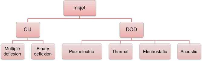
Figure 2.16 Inkjet technology.
CIJ (Continuous Inkjet) Printing
The CIJ technology consists of the generation and the ejection of continuous drops. Those droplets pass through an electrostatic charging electrode and then a high-voltage deflector plate leads trajectory deviation toward a recycling recipient. Two different categories of CIJ have been developed: the binary and the multiple deflections. In a binary deflection system (Figure 2.17) there are two states regulated by the electrostatic deflector. The drops that are charged during the printing step are going directly to the substrate and the non-charged ones are deviated and collected in a gutter and then recycled. In a multiple deflection system, the non-charged drops go to the gutter to be reprocessed while the charged drops are deviated to be deposited onto the substrate.
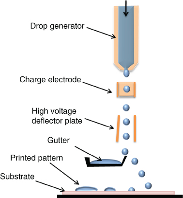
Figure 2.17 Binary continuous inkjet system.
CIJ technology is used in industry for marking and encoding the products before commercialization. It presents advantages such as good printing resolution down to 50 µm, high ejection frequencies of droplets up to 60 kHz at high printing speed, and good process stability without nozzles clogging. However, this technique shows limitations regarding the type of inks to be printed, which have to match the requirements of the system especially for the electrostatic charging step. The ink recycling step can induce materials contamination. Finally, printing of complex designs and customization is not easy because of the continuous ejection of the drops. This is why this technology has never been adopted for printed electronics.
(DOD) Drop-On-Demand Inkjet Printing
The drop-on-demand technique can be divided into four categories: piezoelectric, thermal, electrostatic, and acoustic inkjet. Thermal and piezoelectric inkjets are the most successful technologies adopted in industry and laboratories.
In thermal inkjet, the heating element is integrated within the printhead chamber. A local increase in the temperature of the ink, generally up to 300 °C, creates an air bubble within the ink inside the ejection chamber. This change in local pressure provokes the formation and the ejection of individual droplets (Figure 2.18a). Today, thermal inkjet is widely used for graphic printing and especially for home printers. However, requirements for heating before ejection make this technology very limited in terms of inks. A few studies mentioned the possibility of fabricating biosensors [59, 60]. For instance, Setti et al. [61] reported fabricating an amperometric sensor for the detection of glucose.

Figure 2.18 (a) Thermal inkjet and (b) drop-on-demand inkjet process.
The piezoelectric inkjet technology is based on the use of a piezo membrane (Figure 2.18b). This membrane is mechanically deformed when an external voltage is applied thus causing a change in the pressure inside the printhead chamber. This causes the formation of the droplet in the aperture in the printhead. The jetting of the ink is given by the pressure release and a large type of inks can be used. Here, the nozzle generates a droplet with a volume of a few picoliters. The ink viscosity ranges from 5 to 20 cP and the resolution down to 20 µm.
With the rise in printed electronics, several companies such as FujiFilm, Ceradrop, and Meyer Burger developed new inkjet machines that can print different functional materials using piezo-DOD technology (Figure 2.19). The printing parameters such as the voltage applied to the piezo element, the drop spacing, the waveform, and the temperature of the ink can be tuned. Some printers offer the possibility to realize the alignment to print complete devices with several layers and different inks. The machines show flexibility and are easy to use, making the process adaptable to different materials.
Figure 2.19 Inkjet printer using Clevios™ ink.
(Reproduced with permission from Heraeus.)
Inkjet offers many possibilities for new developments. In the literature, inkjet is widely studied for electronic applications such as for organic thin-film transistors (OTFTs) [62, 63], OLEDs and solar cells or organic photovoltaics (OPVs) [64–68], and sensors [69]. Studies demonstrated the feasibility of using commercial PEDOT:PSS ink to print OTFTs with dimensions in the range of micrometer [70, 71] and sub-micrometer [72] scales by controlling the hydrophobicity of the substrate. Bharathan et al. [73] combined inkjet with spin-coating to pattern electroluminescent devices. Inkjet has also been used to print active layers of solar cells [74, 75] with device efficiency above 3%. Printed conducting polymers have also been studied for chemical sensing such as ammonia detection [76, 77].
2.3.2.2.3 Printability Requirements
In the DOD technology, the formation and ejection of the droplet depend on different rheological parameters of the ink such as viscosity, density, and surface tension (Figure 2.20).

Figure 2.20 (a) Drop formation in the nozzle and (b) ejection of the drop.
(JetXpert drop watcher. Reproduced with permission.)
Printability of the ink depends on these rheological parameters combined with the characteristics of the printhead (nozzle diameter, frequency of the drops’ ejection, applied voltage, channel length, and internal pressure). The rheological behavior of the ink can be described with dimensionless parameters such as the Reynolds number and the Weber number or the Ohnesorge number, defined as
where μ is the viscosity of the ink, ![]() is the density,
is the density, ![]() is the surface tension, R is the radius of the nozzle, and
is the surface tension, R is the radius of the nozzle, and ![]() is the velocity.
is the velocity.
These numbers are directly dependent on the fluid’s rheological properties and they are used to predict the ejection of the ink from the nozzle. In the 1980s, Fromm [78] defined the criteria for ink printability such as ![]() . Later, Reis and Derby [79, 80] discussed Fromm’s assumption and propose their own rheological requirements for ink jetting. Using a numerical simulation of drop formation, Reis suggested that the condition
. Later, Reis and Derby [79, 80] discussed Fromm’s assumption and propose their own rheological requirements for ink jetting. Using a numerical simulation of drop formation, Reis suggested that the condition ![]() is more adapted in order to match the ink with the printing requirements. They propose a chart [80] where one can define which area is the most adequate combing the above-mentioned dimensionless number with DOD printing. The lower limit corresponds to a high viscosity domain that prevents the jetting while the upper limit causes the formation of unwanted satellite drops. This theory is often used in the literature [81–83] for the formulation of new functional inks dedicated to inkjet printing technology.
is more adapted in order to match the ink with the printing requirements. They propose a chart [80] where one can define which area is the most adequate combing the above-mentioned dimensionless number with DOD printing. The lower limit corresponds to a high viscosity domain that prevents the jetting while the upper limit causes the formation of unwanted satellite drops. This theory is often used in the literature [81–83] for the formulation of new functional inks dedicated to inkjet printing technology.
2.3.3 Inks
Graphic inks are widely present on the market and used in daily life. Over the last few years, with concern over environmental issues and to reduce the fabrication costs of electronic components, a new trend has emerged in formulating new functional inks that exhibit different electrical properties. Manufacturers are developing new inks with specific functions that can fit specific requirements for diverse applications such as photovoltaics or thin film transistors (TFTs). In this section, we describe the different categories of inks.
2.3.3.1 Metallic Inks
The inks are usually composed of metallic nanoparticles, for instance, gold, silver, or copper in suspension in solvents. Surfactants can be added to the formulation for the tuning of surface tension to fit the requirements of the printing process. Many manufacturers offer a large choice of metallic inks for printing processes and the market is in expansion. Different methods exist to produce nanoparticles, such as chemical reactions or mechanical attrition. The first method is based on the use of precursors [84] where an organic complex containing metal salt is dissolved in a solvent. For the mechanical attrition, ball milling [85] is usually used to downscale materials to nanoscale. The size of nanoparticles can vary from a few to hundreds of nanometers and they can be produced in different shapes such as nanoplates or nanospheres depending on the preparation conditions. These nanoparticles are subsequently embedded in organic shell polymers for protection against the oxidation and for solubility in water or in vehicle solvents. Poly(vinyl pyrrolidone) (PVP), for example, is one of the most commonly used polymers for the encapsulation of nanoparticles.
Thermal curing is a key step in the fabrication of metal structures. After printing, an annealing step allows the evaporation of organic compounds and the coalescence of nanoparticles. New types of selective curing techniques such as microwave curing [86], laser sintering [87], or photonic sintering [88] permit the coalescence of nanoparticles without thermomechanical degradation or damage to underlying materials such as plastic substrates. Electrical conductivity of between 10% and 30% of that of bulk metal is generally obtained, depending on the thermal cycle and the size and the shape of the nanoparticles [89].
2.3.3.2 Dielectric Inks
Dielectric inks are usually used in printed electronics to fabricate dielectric isolation layers in circuits. They can be UV-based inks also composed of nanoparticles (TiO2, BaTiO3). UV-curable inks comprise monomers, oligomers, photoinitiators, and additives [90]. Photoinitiators absorb energy from UV leading to the polymerization of the monomers, for instance, acrylic monomers after exposure to UV light (Figure 2.21).
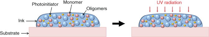
Figure 2.21 UV polymerization.
These UV inks offer advantages such as facile processing without clogging the nozzle. They avoid the evaporation of volatile organic compounds from the ink since polymerization occurs without the need for a drying step. The polymerization step takes a few seconds and can be easily integrated in a roll-to-roll process.
2.3.3.3 Conducting Polymer Inks
Since their discovery in the 1970s by Shirakawa et al. [91], conducting polymers have been broadly studied because of their electrical conductivity, high mechanical flexibility, and long-term stability. With the emergence of printed electronics, conducting polymers are formulated in new conducting inks. Polyaniline, polypyrroles, polythiophenes, and PEDOT:PSS are especially considered for electronic applications. They are dispersed in organic solvents, and secondary dopant solvents such as ethylene glycol or dimethyl sulfoxide (DMSO) are added to the formulation to boost the conductivity and to fix the viscosity while surfactants such as Triton X-100 adapt the surface tension to match the substrate surface energy.
Polypyrrole is a dielectric polymer that can be doped by oxidation process to reach conductivity up to 100 S cm−1 [92]. This polymer is usually electrochemically deposited [93] for applications such as capacitors [94] or chemical sensors [95]. Only few studies mention polypyrrole as an ink [96, 97] for printed electronics applications.
Polyaniline is a conducting polymer that combines electronic and optical properties. Polyaniline exists in three stable oxidation states that exhibit different conductivities and colors. Among them, the emeraldine state presents the highest conductivity in its doped state. Polyaniline has advantages such as stability at room temperature, ease of synthesis, and transparency. Companies such as Panipol are developing polyaniline inks compatible with inkjet and others process. This polymer has been studied for applications such as gas sensing [98], especially ammonia [77, 99], combined with graphene for capacitor electrodes [100] and recently for biomedical applications such as biosensors [101, 102]. However, this polymer is not compatible [103] for implantable biodevices.
PEDOT in its neutral state is a conducting polymer but remains difficult to process mostly because it is insoluble and rapidly oxidizes in air. In combination with PSS, a water-soluble polymer that serves as a charge-balancing counter ion [104], the complex is stable in solution. In its oxidized state, PEDOT:PSS is a stable polymer and it is one of the most studied polymers currently used for printing transparent electrodes [105] or hole transport layers [35] in applications such as solar cells and OLEDs. PEDOT:PSS inks are available commercially in water-based formulations from a few suppliers such as Heraeus and Agfa (Orgacon) that are compatible with printing technologies such as inkjet or screen printing. PEDOT:PSS thin films present high transparency, good thermal stability, and high conductivity, which can be even tuned by doping the polymer with solvents [106]. Recent research [107, 108] highlights PEDOT:PSS as a good candidate for biomedical applications owing to its higher electronic and ionic properties combined with its biocompatibility[109].
2.3.4 Comparison of Printing Techniques
In this section, we focus on specific characteristics of printing technologies (Table 2.1). Screen printing is one of the most advanced techniques in terms of research and development for printed electronics. It allows depositing highly viscous inks resulting in thicker layers than other printing techniques and can fit many electronic applications. It is a mature technology that is already used in industry today. This prerequisite could be achieved by other techniques such as gravure printing by optimizing the size of the engraved cells to reach the micron scale. Both flexography and gravure show promising future in electronics but limits still exist such as the manufacturing costs for gravure or the presence of the halo for the flexography. A compromise must be found between thickness and resolution.
Table 2.1 Comparison of printing techniques.
| Gravure | Flexography | Screen printing | Aerosol jet | Inkjet | |
| Printing form | Cylinder engraved | Printing plate | Mesh screen | Digital | Digital |
| Speed (m min−1) | 8–100 | 5–180 | 30–100 | 1.2 | 0.02–0.5 |
| Resolution (µm) | 20 | 50 | <100 | 10 | 20 |
| Viscosity (cP) | 10–500 | 10–100 | 500–10 000 | 1–2500 | 5–20 |
| Thickness (µm) | 1–8 | 1 | >10 | >0.1 | 0.1–15 |
Inkjet is a promising technique especially at the laboratory scale as it allows the digital fabrication of complete devices with low manufacturing costs. Additionally, the geometry can be customized on demand. This technique is easy to use to evaluate new designs and inks. Today, inkjet printing is still difficult to use in roll-to-roll processes because of maintenance issues related to nozzle clogging and ink stability. The printing resolution is limited by the rheology of the ink, the characteristics of the printhead, and the physicochemical properties of the substrate. On the other hand, Aerosol jet printing is a recent technique that is versatile and customizable, and could offer an alternative to other processes as it shows flexibility in terms of compatibility with inks (viscosity). The resolution is higher than inkjet but it requires further developments to compete with actual fabrication processes.
2.4 Conclusions
Photolithography has been the technique of choice for device fabrication in the semiconductor industry for many years now. It is a relatively simple, reliable, and reproducible way of fabricating electronic devices in a cost-effective and controllable manner. It can offer high-resolution patterning and the degree of freedom coming from its potential of scalability to large-area substrates. The aforementioned, together with the high throughput that comes hand in hand with its parallel nature, are the technique’s comparative advantages over other proposed approaches. Shadow mask evaporation and soft or hard imprint, which were recruited to replace photolithography, do not seem able to compete with it on one or more of its previously mentioned strong points. In addition, one of the drawbacks that these processes share is the issue of registration, a figure of merit that photolithography can easily offer. Above all, photolithography is an appealing organic material patterning technique as it promises to use the knowhow and the added knowledge of the already well-established and mature semiconductor industry.
Photolithography’s main challenge, though, remains its implementation in the organic world. Incompatibility issues between the organic materials and the chemicals used during the process have been widely discussed in this chapter along with possible ways to circumvent this problem. Moreover, lithographic patterning requires a controlled environment and consequently clean room facilities. This fact may render the fabrication process a rather complicated one, an issue that can be addressed, nevertheless, by the use of the already existing semiconductor production line. Provided that the proposed organic patterning approaches will be optimized to become generic, versatile, and applicable to any organic material, photolithography has the potential to be the technique of choice in polymer device fabrication for the years to come.
On the other hand, printed technologies also present many advantages such as versatility, flexibility, and low cost. They are compatible with a wide range of materials to formulate inks such as conducting polymers, for instance. They can be sheet-based or roll-to-roll techniques and can use flexible plastics as substrates. They can operate at high speed. They offer new perspectives for electronic applications (OFETS, OLEDs, bioelectronics, etc.) but require further development to reach high resolution.
References
- 1 Malliaras, G. and Friend, R. (2005) An organic electronics primer. Phys. Today , 58 (5), 53–58.
- 2 Forrest, S.R. (2004) The path to ubiquitous and low-cost organic electronic appliances on plastic. Nature , 428 (6986), 911–918.
- 3 Sessolo, M. et al. (2013) Easy-to-fabricate conducting polymer microelectrode arrays. Adv. Mater. , 25 (15), 2135–2139.
- 4 DeFranco, J.A. et al. (2006) Photolithographic patterning of organic electronic materials. Org. Electron. , 7 (1), 22–28.
- 5 Taylor, P.G. et al. (2009) Orthogonal patterning of PEDOT:PSS for organic electronics using hydrofluoroether solvents. Adv. Mater. , 21 (22), 2314–2317.
- 6 Huang, J. et al. (2007) Patterning of organic devices by interlayer lithography. J. Mater. Chem. , 17 (11), 1043–1049.
- 7 Madou, M.J. (2011) Manufacturing Techniques for Microfabrication and Nanotechnology , Taylor & Francis.
- 8 Wilson, C.G. , Dammel, R.R. , and Reiser, A. (1997) Photoresist Materials: A Historical Perspective, Proc. SPIE , (3049), 28–41.
- 9 Bahreyni, B. (2009) in Fabrication and Design of Resonant Microdevices (ed. B. Bahreyni ), William Andrew Publishing, Norwich, NY, pp. 9–46.
- 10 Levinson, H.J. (2005) Principles of Lithography , Society of Photo Optical.
- 11 Thompson, L.F. , Willson, C.G. , and Bowden, M.J. (1983) Introduction to Microlithography , American Chemical Society, Washington, DC.
- 12 Mack, C. (2008) Fundamental Principles of Optical Lithography: the Science of Microfabrication , John Wiley & Sons, Ltd.
- 13 Ilic, B. and Craighead, H.G. (2000) Topographical patterning of chemically sensitive biological materials using a polymer-based dry lift off. Biomed. Microdevices , 2 (4), 317–322.
- 14 Kymissis, I. , Dimitrakopoulos, C.D. , and Purushothaman, S. (2002) Patterning pentacene organic thin film transistors. J. Vac. Sci. Technol., B , 20 (3), 956.
- 15 Khodagholy, D. et al. (2011) Highly conformable conducting polymer electrodes for In vivo recordings. Adv. Mater. , 23 (36), H268–H272.
- 16 Chang, T.Y. et al. (2007) Cell and protein compatibility of parylene-C surfaces. Langmuir , 23 (23), 11718–11725.
- 17 Fortin, J.B. and Lu, T.-M. (2000) Mass spectrometry study during the vapor deposition of poly-para-xylylene thin films. J. Vac. Sci. Technol., A , 18 (5), 2459–2465.
- 18 Zakhidov, A.A. et al. (2008) Hydrofluoroethers as orthogonal solvents for the chemical processing of organic electronic materials. Adv. Mater. , 20 (18), 3481–3484.
- 19 Hwang, H.S. et al. (2008) Dry photolithographic patterning process for organic electronic devices using supercritical carbon dioxide as a solvent. J. Mater. Chem. , 18 (26), 3087–3090.
- 20 Das, R. and Harrop, P. (2013) Printed, Organic & Flexible Electronics: Forecasts, Players & Opportunities 2009–2029 , IDTechEx, Cambridge.
- 21 Pudas, M. , Hagberg, J. , and Leppävuori, S. (2004) Gravure offset printing of polymer inks for conductors. Prog. Org. Coat. , 49 (4), 324–335.
- 22 Voigt, M.M. et al. (2010) Polymer field-effect transistors fabricatfed by the sequential gravure printing of polythiophene, two insulator layers, and a metal Ink gate. Adv. Funct. Mater. , 20 (2), 239–246.
- 23 Kopola, P. et al. (2011) Gravure printed flexible organic photovoltaic modules. Sol. Energy Mater. Sol. Cells , 95 (5), 1344–1347.
- 24 Hübler, A. et al. (2011) Printed paper photovoltaic cells. Adv. Energy Mater. , 1 (6), 1018–1022.
- 25 Ding, J.M. et al. (2009) Patternable polymer bulk heterojunction photovoltaic cells on plastic by rotogravure printing. Sol. Energy Mater. Sol. Cells , 93 (4), 459–464.
- 26 Yang, J. et al. (2013) Organic photovoltaic modules fabricated by an industrial gravure printing proofer. Sol. Energy Mater. Sol. Cells , 109, 47–55.
- 27 Reddy, A.S.G. et al. (2011) Gravure printed electrochemical biosensor. Procedia Eng. , 25, 956–959.
- 28 Mäkelä, T. et al. (2007) Continuous roll to roll nanoimprinting of inherently conducting polyaniline. Microelectron. Eng. , 84 (5–8), 877–879.
- 29 Søndergaard, R.R. , Hösel, M. , and Krebs, F.C. (2013) Roll-to-Roll fabrication of large area functional organic materials. J. Polym. Sci., Part B: Polym. Phys. , 51 (1), 16–34.
- 30 Hübler, A.C. et al. (2011) Three-dimensional integrated circuit using printed electronics. Org. Electron. , 12 (3), 419–423.
- 31 Krebs, F.C. , Fyenbo, J. , and Jørgensen, M. (2010) Product integration of compact roll-to-roll processed polymer solar cell modules: methods and manufacture using flexographic printing, slot-die coating and rotary screen printing. J. Mater. Chem. , 20 (41), 8994–9001.
- 32 Yu, J.-S. et al. (2012) Silver front electrode grids for ITO-free all printed polymer solar cells with embedded and raised topographies, prepared by thermal imprint, flexographic and inkjet roll-to-roll processes. Nanoscale , 4 (19), 6032–6040.
- 33 Kamholz, R. (2013) Andy Warhol and His Process , http://www.sothebys.com/en/news-video/blogs/all-blogs/21-days-of-andy-warhol/2013/11/andy-warhol-and-his-process.html (accessed 29 March 2017).
- 34 Shaheen, S.E. et al. (2001) Fabrication of bulk heterojunction plastic solar cells by screen printing. Appl. Phys. Lett. , 79 (18), 2996–2998.
- 35 Krebs, F.C. et al. (2009) A complete process for production of flexible large area polymer solar cells entirely using screen printing—first public demonstration. Sol. Energy Mater. Sol. Cells , 93 (4), 422–441.
- 36 Krebs, F.C. (2009) All solution roll-to-roll processed polymer solar cells free from indium-tin-oxide and vacuum coating steps. Org. Electron. , 10 (5), 761–768.
- 37 Gray, C. et al. (2001) Screen Printed Organic Thin Film Transistors (OTFTs) on a Flexible Substrate, In International Symposium on Optical Science and Technology (pp. 89–94). International Society for Optics and Photonics .
- 38 Pardo, D.A. , Jabbour, G.E. , and Peyghambarian, N. (2000) Application of screen printing in the fabrication of organic light-emitting devices. Adv. Mater. , 12 (17), 1249–1252.
- 39 Jabbour, G.E. , Radspinner, R. , and Peyghambarian, N. (2001) Screen printing for the fabrication of organic light-emitting devices. IEEE J. Sel. Top. Quantum Electron. , 7 (5), 769–773.
- 40 Lee, D.-H. et al. (2008) Single-layer organic-light-emitting devices fabricated by screen printing method. Korean J. Chem. Eng. , 25 (1), 176–180.
- 41 Tudorache, M. and Bala, C. (2007) Biosensors based on screen-printing technology, and their applications in environmental and food analysis. Anal. Bioanal.Chem. , 388 (3), 565–578.
- 42 O’Halloran, M.P. , Pravda, M. , and Guilbault, G.G. (2001) Prussian Blue bulk modified screen-printed electrodes for H 2 O 2 detection and for biosensors. Talanta , 55 (3), 605–611.
- 43 Albareda-Sirvent, M. , Merkoçi, A. , and Alegret, S. (2000) Configurations used in the design of screen-printed enzymatic biosensors. A review. Sens. Actuators, B , 69 (1–2), 153–163.
- 44 Hill, H.A.O. et al. (1998) Strip electrode with screen printing. Google Patents, U.S. Patent No 5,820,551.
- 45 Hill, H.A.O. et al. (1996) Strip electrode including screen printing of a single layer. Google Patents, U.S. Patent No 5,509,410.
- 46 Su, C.S. et al. (2006) Electrochemical biosensor by screen printing and method of fabricating same. Google Patents, U.S. Patent No 7,138,041.
- 47 Krebs, F.C. (2009) Fabrication and processing of polymer solar cells: a review of printing and coating techniques. Sol. Energy Mater. Sol. Cells , 93 (4), 394–412.
- 48 Kopola, P. et al. (2012) Aerosol jet printed grid for ITO-free inverted organic solar cells. Sol. Energy Mater. Sol. Cells , 107, 252–258.
- 49 Girotto, C. et al. (2009) Exploring spray coating as a deposition technique for the fabrication of solution-processed solar cells. Sol. Energy Mater. Sol. Cells , 93 (4), 454–458.
- 50 Cho, J.H. et al. (2008) Printable ion-gel gate dielectrics for low-voltage polymer thin-film transistors on plastic. Nat. Mater. , 7 (11), 900–906.
- 51 Ingo, G. et al. (2010) Surface biofunctionalization and production of miniaturized sensor structures using aerosol printing technologies. Biofabrication , 2 (1), 014106.
- 52 Strutt, J.W. and Rayleigh, L. (1878) On the instability of jets. Proc. London Math. Soc , 10, 4–13.
- 53 Rune, E. (1951) Measuring instrument of the recording type. Google Patents, U.S. Patent No 2,566,443.
- 54 Sweet, R.G. (1965) High frequency recording with electrostatically deflected ink jets. Rev. Sci. Instrum. , 36 (2), 131–136.
- 55 Zoltan, S.I. (1972) Pulsed droplet ejecting system. Google Patents, U.S. Patent No 3,683,212.
- 56 Kyser, E.L. and Sears, S.B. (1976) Method and apparatus for recording with writing fluids and drop projection means therefore. Google Patents, U.S. Patent No. 3,946,398.
- 57 Donald, D.K. , Lee, M.J. , and Vaught, J.L. (1982) Method and apparatus for drop-on-demand ink jet printing. Google Patents, U.S. Patent No 4,336,544.
- 58 Endo, I. et al. (1988) Bubble jet recording method and apparatus in which a heating element generates bubbles in a liquid flow path to project droplets. Google Patents, U.S. Patent No 4,723,129.
- 59 Setti, L. et al. (2004) Thermal inkjet technology for the microdeposition of biological molecules as a viable route for the realization of biosensors. Anal. Lett. , 37 (8), 1559–1570.
- 60 Setti, L. et al. (2007) An HRP-based amperometric biosensor fabricated by thermal inkjet printing. Sens. Actuators, B , 126 (1), 252–257.
- 61 Setti, L. et al. (2005) An amperometric glucose biosensor prototype fabricated by thermal inkjet printing. Biosens. Bioelectron. , 20 (10), 2019–2026.
- 62 Arias, A. et al. (2004) All jet-printed polymer thin-film transistor active-matrix backplanes. Appl. Phys. Lett. , 85 (15), 3304–3306.
- 63 Sirringhaus, H. , Kawase, T. , and Friend, R.H. (2001) High-resolution ink-Jet printing of all-polymer transistor circuits. MRS Bull. , 26 (07), 539–543.
- 64 Hebner, T.R. et al. (1998) Ink-jet printing of doped polymers for organic light emitting devices. Appl. Phys. Lett. , 72 (5), 519–521.
- 65 Shimoda, T. et al. (2003) Inkjet printing of light-emitting polymer displays. MRS Bull. , 28 (11), 821–827.
- 66 Aernouts, T. et al. (2008) Polymer based organic solar cells using ink-jet printed active layers. Appl. Phys. Lett. , 92 (3), 033306.
- 67 Eom, S.H. et al. (2009) Polymer solar cells based on inkjet-printed PEDOT:PSS layer. Org. Electron. , 10 (3), 536–542.
- 68 Hoth, C.N. et al. (2007) High photovoltaic performance of inkjet Printed polymer:fullerene blends. Adv. Mater. , 19 (22), 3973–3978.
- 69 Abe, K. , Suzuki, K. , and Citterio, D. (2008) Inkjet-printed microfluidic multianalyte chemical sensing paper. Anal. Chem. , 80 (18), 6928–6934.
- 70 Sirringhaus, H. et al. (2000) High-resolution inkjet printing of all-polymer transistor circuits. Science , 290 (5499), 2123–2126.
- 71 Kawase, T. et al. (2003) Inkjet printing of polymer thin film transistors. Thin Solid Films , 438–439, 279–287.
- 72 Wang, J.Z. et al. (2004) Dewetting of conducting polymer inkjet droplets on patterned surfaces. Nat. Mater. , 3 (3), 171–176.
- 73 Bharathan, J. and Yang, Y. (1998) Polymer electroluminescent devices processed by inkjet printing: I. Polymer light-emitting logo. Appl. Phys. Lett. , 72 (21), 2660–2662.
- 74 Steirer, K.X. et al. (2009) Ultrasonically sprayed and inkjet printed thin film electrodes for organic solar cells. Thin Solid Films , 517 (8), 2781–2786.
- 75 Hoth, C.N. et al. (2008) Printing highly efficient organic solar cells. Nano Lett. , 8 (9), 2806–2813.
- 76 Jang, J. , Ha, J. , and Cho, J. (2007) Fabrication of water-dispersible polyaniline-poly(4-styrenesulfonate) nanoparticles for inkjet-printed chemical-sensor applications. Adv. Mater. , 19 (13), 1772–1775.
- 77 Crowley, K. et al. (2008) Fabrication of an ammonia gas sensor using inkjet-printed polyaniline nanoparticles. Talanta , 77 (2), 710–717.
- 78 Fromm, J.E. (1984) Numerical calculation of the fluid dynamics of drop-on-demand jets. IBM J. Res. Dev. , 28 (3), 322–333.
- 79 Reis, N. and Derby, B. (2000) Ink Jet deposition of ceramic suspensions: modeling and experiments of droplet formation. MRS Proceedings. Cambridge University Press , 625, 117–122.
- 80 Derby, B. (2010) Inkjet printing of functional and structural materials: fluid property requirements, feature stability, and resolution. Annu. Rev. Mater. Res. , 40, 395–414.
- 81 Denneulin, A. et al. (2011) Impact of ink formulation on carbon nanotube network organization within inkjet printed conductive films. Carbon , 49 (8), 2603–2614.
- 82 Angelo, P.D. and Farnood, R.R. (2010) Poly (3, 4-ethylenedioxythiophene): poly (styrene sulfonate) inkjet inks doped with carbon nanotubes and a polar solvent: the effect of formulation and adhesion on conductivity. J. Adhes. Sci. Technol. , 24 (3), 643–659.
- 83 Aleeva, Y. and Pignataro, B. (2014) Recent advances in upscalable wet methods and ink formulations for printed electronics. J. Mater. Chem. C , 2 (32), 6436–6453.
- 84 Grouchko, M. and Magdassi, S. (2013) Inks containing metal precursors nanoparticles. Google Patents U.S. Patent Application No. 14/382,110.
- 85 Park, B.K. et al. (2007) Direct writing of copper conductive patterns by ink-jet printing. Thin Solid Films , 515 (19), 7706–7711.
- 86 Perelaer, J. , de Gans, B.-J. , and Schubert, U.S. (2006) Ink-jet printing and microwave sintering of conductive silver tracks. Adv. Mater. Deerfield Beach Then Weinheim-, 18 (16), 2101.
- 87 Seung, H.K. et al. (2007) All-inkjet-printed flexible electronics fabrication on a polymer substrate by low-temperature high-resolution selective laser sintering of metal nanoparticles. Nanotechnology , 18 (34), 345202.
- 88 Kim, H.-S. et al. (2009) Intense pulsed light sintering of copper nanoink for printed electronics. Appl. Phys. A , 97 (4), 791–798.
- 89 Dick, K. et al. (2002) Size-dependent melting of silica-encapsulated gold nanoparticles. J. Am. Chem. Soc. , 124 (10), 2312–2317.
- 90 Go, E.C. (2009) Effects of Oligomer-to-Monomer Ratio on Ink Film Properties of White UV-Curable Gravure Ink for Printing on Biaxially Oriented Polypropylene (BOPP) , Rochester Institute of Technology.
- 91 Shirakawa, H. et al. (1977) Synthesis of electrically conducting organic polymers: halogen derivatives of polyacetylene,(CH) x. J. Chem. Soc., Chem. Commun. , (16), 578–580.
- 92 Beck, F. and Oberst, M. (1992) Electrocatalytic deposition of polypyrrole in the presence of bromide. J. Appl. Electrochem. , 22 (4), 332–340.
- 93 Li, C. et al. (2005) Electrochemical thin film deposition of polypyrrole on different substrates. Surf. Coat. Technol. , 198 (1), 474–477.
- 94 Muthulakshmi, B. et al. (2006) Electrochemical deposition of polypyrrole for symmetric supercapacitors. J. Power Sources , 158 (2), 1533–1537.
- 95 Ramanavičius, A. , Ramanavičienė, A. , and Malinauskas, A. (2006) Electrochemical sensors based on conducting polymer—polypyrrole. Electrochim. Acta , 51 (27), 6025–6037.
- 96 Mabrook, M.F. , Pearson, C. , and Petty, M.C. (2006) Inkjet-printed polypyrrole thin films for vapour sensing. Sens. Actuators, B , 115 (1), 547–551.
- 97 Gangopadhyay, R. and Molla, M.R. (2011) Polypyrrole–polyvinyl alcohol stable nanodispersion: a prospective conducting black ink. J. Polym. Sci., Part B: Polym. Phys. , 49 (11), 792–800.
- 98 Loffredo, F. et al. (2007) Gas sensor devices obtained by ink-jet printing of polyaniline suspensions, in Macromolecular Symposia , Wiley Online Library.
- 99 Hibbard, T. , Crowley, K. , and Killard, A.J. (2013) Direct measurement of ammonia in simulated human breath using an inkjet-printed polyaniline nanoparticle sensor. Anal. Chim. Acta , 779, 56–63.
- 100 Xu, Y. et al. (2013) Screen-printable thin film supercapacitor device utilizing graphene/polyaniline inks. Adv. Energy Mater. , 3 (8), 1035–1040.
- 101 Morrin, A. et al. (2005) Novel biosensor fabrication methodology based on processable conducting polyaniline nanoparticles. Electrochem. Commun. , 7 (3), 317–322.
- 102 Dionisi, A. et al. (2014) Biocompatible inkjet resistive sensors for biomedical applications. 2014 IEEE International Instrumentation and Measurement Technology Conference (I2MTC) Proceedings, IEEE.
- 103 Huang, L. et al. (2008) Synthesis of biodegradable and electroactive multiblock polylactide and aniline pentamer copolymer for tissue engineering applications. Biomacromolecules , 9 (3), 850–858.
- 104 Skotheim, T.A. and Reynolds, J. (2006) Conjugated Polymers: Theory, Synthesis, Properties, and Characterization , Taylor & Francis.
- 105 Cho, C.-K. et al. (2011) Mechanical flexibility of transparent PEDOT:PSS electrodes prepared by gravure printing for flexible organic solar cells. Sol. Energy Mater. Sol. Cells , 95 (12), 3269–3275.
- 106 Kim, J.Y. et al. (2002) Enhancement of electrical conductivity of poly(3,4-ethylenedioxythiophene)/poly(4-styrenesulfonate) by a change of solvents. Synth. Met. , 126 (2–3), 311–316.
- 107 Leleux, P. et al. (2014) Conducting polymer electrodes for electroencephalography. Adv. Healthc. Mater. , 3 (4), 490–493.
- 108 Khodagholy, D. et al. (2013) In vivo recordings of brain activity using organic transistors. Nat. Commun. , 4, 1575.
- 109 Berggren, M. and Richter-Dahlfors, A. (2007) Organic bioelectronics. Adv. Mater. , 19 (20), 3201–3213.