
Chapter 3
Conversion
3.1 Introduction to conversion
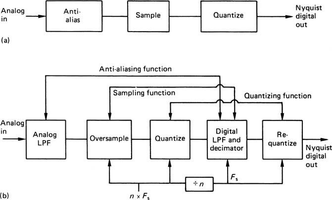
The most useful and therefore common signal representation is pulse code modulation or PCM which was introduced in Chapter 1. The input is a continuous-time, continuous-voltage video waveform, and this is converted into a discrete-time, discrete-voltage format by a combination of sampling and quantizing. As these two processes are independent they can be performed in either order. Figure 3.1(a) shows an analog sampler preceding a quantizer, whereas (b) shows an asynchronous quantizer preceding a digital sampler.
Figure 3.1 Since sampling and quantizing are orthogonal, the order in which they are performed is not important. In (a) sampling is performed first and the samples are quantized. This is common in audio convertors. In (b) the analog input is quantized into an asynchronous binary code. Sampling takes place when this code is latched on sampling clock edges. This approach is universal in video convertors.

The independence of sampling and quantizing allows each to be discussed quite separately in some detail, prior to combining the processes for a full understanding of conversion.
3.2 Sampling and aliasing
Sampling can take place in space or time and in several dimensions at once. Figure 3.2 shows that in temporal sampling the frequency of the signal to be sampled and the sampling rate Fs are measured in Hertz (Hz). In still images there is no temporal change and Figure 3.2 also shows that the sampling is spatial. The sampling rate is now a spatial frequency. The absolute unit of spatial frequency is cycles per metre, although for imaging purposes cycles-per-mm is more practical. Spatial and temporal frequencies are related by the process of scanning as given by:
Figure 3.2 (a) Electrical waveforms are sampled temporally at a sampling rate measured in Hz. (b) Image information must be sampled spatially, but there is no single unit of spatial sampling frequency. (c) The acuity of the eye is measured as a subtended angle, and here two different displays of different resolutions give the same result at the eye because they are at a different distance. (d) Size-independent units such as cycles per picture height will also be found.
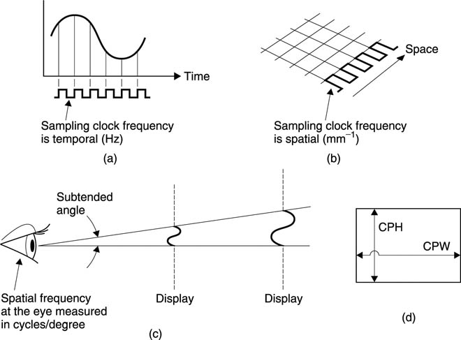
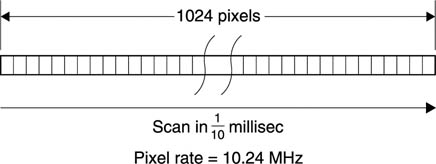
Figure 3.3 shows that if the 1024 pixels along one line of an SVGA monitor were scanned in one tenth of a millisecond, the sampling clock frequency would be 10.24 MHz.
Figure 3.3 The connection between image resolution and pixel rate is the scanning speed. Scanning the above line in 1/10ms produces a pixel rate of 10.24 MHz.
The sampling process originates with a pulse train which is shown in Figure 3.4(a) to be of constant amplitude and period. This pulse train can be temporal or spatial. The information to be sampled amplitude-modulates the pulse train in much the same way as the carrier is modulated in an AM radio transmitter. It is important to avoid overmodulating the pulse train as shown in (b) and this is achieved by suitably biasing the information waveform as at (c).
Figure 3.4 The sampling process requires a constant-amplitude pulse train as shown in (a). This is amplitude modulated by the waveform to be sampled. If the input waveform has excessive amplitude or incorrect level, the pulse train clips as shown in (b). For a bipolar waveform, the greatest signal level is possible when an offset of half the pulse amplitude is used to centre the waveform as shown in (c).

In the same way that AM radio produces sidebands or identical images above and below the carrier, sampling also produces sidebands although the carrier is now a pulse train and has an infinite series of harmonics as shown in Figure 3.5(a). The sidebands repeat above and below each harmonic of the sampling rate as shown in (b). As the spectrum of the baseband signal is simply repeated, sampling need not lose any information.
Figure 3.5 (a) Spectrum of sampling pulses. (b) Spectrum of samples. (c) Aliasing due to sideband overlap. (d) Beat-frequency production. (e) 4 × oversampling.

The sampled signal can be returned to the continuous domain simply by passing it into a low-pass filter which prevents the images from passing, hence the term ‘anti-image filter’. If considered in the time domain it can be called a reconstruction filter. It can also be considered as a spatial filter if a sampled still image is being returned to a continuous image. Such a filter will be two-dimensional.
If the input has excessive bandwidth, the sidebands will overlap (Figure 3.5(c)) and the result is aliasing, where certain output frequencies are not the same as their input frequencies but instead become difference frequencies (Figure 3.5(d)). It will be seen that aliasing does not occur when the input bandwidth is equal to or less than half the sampling rate, and this derives the most fundamental rule of sampling, which is that the sampling rate must be at least twice the input bandwidth.
Nyquist1 is generally credited with being the first to point this out (1928), although the mathematical proofs were given independently by Shannon2, 3 and Kotelnikov. It subsequently transpired that Whittaker4 beat them all to it, although his work was not widely known at the time. One half of the sampling frequency is often called the Nyquist frequency.
Aliasing can be described equally well in the time domain. In Figure 3.6(a) the sampling rate is obviously adequate to describe the waveform, but at (b) it is inadequate and aliasing has occurred. Where there is no control over the spectrum of input signals it becomes necessary to have a low-pass filter at the input which prevents frequencies of more than half the sampling rate from reaching the sampling stage.
Figure 3.6 In (a), the sampling is adequate to reconstruct the original signal. In (b) the sampling rate is inadequate, and reconstruction produces the wrong waveform (dotted). Aliasing has taken place.

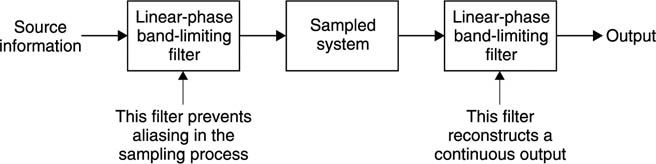
Figure 3.7 shows that all practical sampling systems consist of a pair of filters, the anti-aliasing filter before the sampling process and the reconstruction filter after it. It should be clear that the results obtained will be strongly affected by the quality of these filters which may be spatial or temporal according to the application.
Figure 3.7 Sampling systems depend completely on the use of band limiting filters before and after the sampling stage. Implementing these filters rigorously is non-trivial.
3.3 Reconstruction
Perfect reconstruction was theoretically demonstrated by Shannon as shown in Figure 3.8. The input must be band limited by an ideal linear-phase low-pass filter with a rectangular frequency response and a bandwidth of one-half the sampling frequency. The samples must be taken at an instant with no averaging of the waveform. These instantaneous samples can then be passed through a second, identical filter which will perfectly reconstruct that part of the input waveform which was within the passband.
Figure 3.8 Shannon’s concept of perfect reconstruction requires the hypothetical approach shown here. The anti-aliasing and reconstruction filters must have linear phase and rectangular frequency response. The sample period must be infinitely short and the sample clock must be perfectly regular. Then the output and input waveforms will be identical if the sampling frequency is twice the input bandwidth (or more).

It was shown in Chapter 2 that the impulse response of a linear-phase ideal low-pass filter is a sinx/x waveform, and this is repeated in Figure 3.9(a). Such a waveform passes through zero volts periodically. If the cut-off frequency of the filter is one-half of the sampling rate, the impulse passes through zero at the sites of all other samples. It can be seen from Figure 3.9(b) that at the output of such a filter, the voltage at the centre of a sample is due to that sample alone, since the value of all other samples is zero at that instant. In other words the continuous output waveform must pass through the tops of the input samples. In between the sample instants, the output of the filter is the sum of the contributions from many impulses (theoretically an infinite number), causing the waveform to pass smoothly from sample to sample.
Figure 3.9 An ideal low-pass filter has an impulse response shown in (a). The impulse passes through zero at intervals equal to the sampling period. When convolved with a pulse train at the sampling rate, as shown in (b), the voltage at each sample instant is due to that sample alone as the impulses from all other samples pass through zero there.
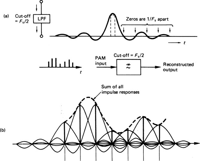
It is a consequence of the band-limiting of the original anti-aliasing filter that the filtered analog waveform could only take one path between the samples. As the reconstruction filter has the same frequency response, the reconstructed output waveform must be identical to the original band-limited waveform prior to sampling. A rigorous mathematical proof of reconstruction can be found in Porat5 or Betts.6
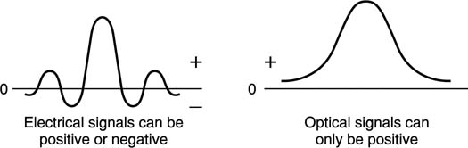
Perfect reconstruction with a Nyquist sampling rate is an ideal limiting condition which can only be approached, but it forms a useful performance target. Zero duration pulses are impossible and the ideal linear-phase filter with a vertical ‘brick-wall’ cut-off slope is impossible to implement. In the case of temporal sampling, as the slope tends to vertical, the delay caused by the filter goes to infinity. In the case of spatial sampling, sharp cut optical filters are impossible to build. Figure 3.10 shows that the spatial impulse response of an ideal lens is a symmetrical intensity function. Note that the function is positive only as the expression for intensity contains a squaring process. The negative excursions of the sinx/x curve can be handled in an analog or digital filter by negative voltages or numbers, but in optics there is no negative light. The restriction to positive only impulse response limits the sharpness of optical filters.
Figure 3.10 In optical systems the spatial impulse response cannot have negative excursions and so ideal filters in optics are more difficult to make.
In practice, real filters with finite slopes can still be used as shown in Figure 3.11. The cut-off slope begins at the edge of the required pass band, and because the slope is not vertical, aliasing will always occur, but the sampling rate can be raised to drive aliasing products to an arbitrarily low level. The perfect reconstruction process still works, but the system is a little less efficient in information terms because the sampling rate has to be raised. There is no absolute factor by which the sampling rate must be raised. A figure of 10 per cent is typical in temporal sampling, although it depends upon the filters which are available and the level of aliasing products that are acceptable.
Figure 3.11 With finite slope filters, aliasing is always possible, but it can be set at an arbitrarily low level by raising the sampling rate.

3.4 Aperture effect
The reconstruction process of Figure 3.9 only operates exactly as shown if the impulses are of negligible duration. In many processes this is not the case, and many real devices keep the analog signal constant for a substantial part of or even the whole period. The result is a waveform which is more like a staircase than a pulse train. The case where the pulses have been extended in width to become equal to the sample period is known as a zero-order hold system and has a 100 per cent aperture ratio.
Whereas pulses of negligible width have a uniform spectrum, which is flat within the baseband, pulses of 100 per cent aperture ratio have a sinx/x spectrum which is shown in Figure 3.12. The frequency response falls to a null at the sampling rate, and as a result is about 4 dB down at the edge of the baseband. If the pulse width is stable, the reduction of high frequencies is constant and predictable, and an appropriate equalization circuit can render the overall response flat once more. An alternative is to use resampling which is shown in Figure 3.13. Resampling passes the zero-order hold waveform through a further synchronous sampling stage which consists of an analog switch that closes briefly in the centre of each sample period. The output of the switch will be pulses which are narrower than the original. If, for example, the aperture ratio is reduced to 50 per cent of the sample period, the first frequency response null is now at twice the sampling rate, and the loss at the edge of the audio band is reduced. As the figure shows, the frequency response becomes flatter as the aperture ratio falls. The process should not be carried too far, as with very small aperture ratios there is little energy in the pulses and noise can be a problem. A practical limit is around 12.5 per cent where the frequency response is virtually ideal.
Figure 3.12 Frequency response with 100 per cent aperture nulls at multiples of sampling rate. Area of interest is up to half sampling rate.
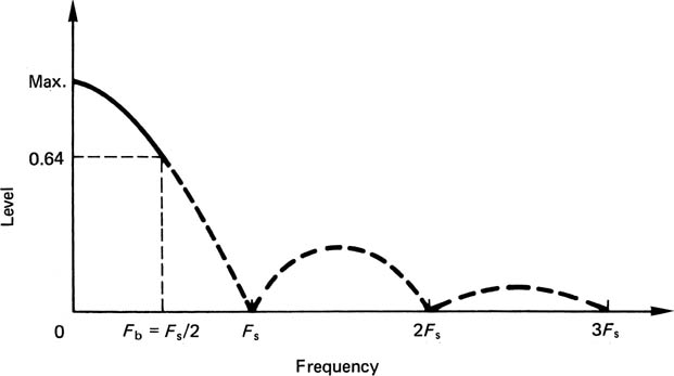
Figure 3.13 (a) Resampling circuit eliminates transients and reduces aperture ratio. (b) Response of various aperture ratios.

The aperture effect will show up in many aspects of television. Lenses have finite MTF (modulation transfer function), such that a very small object becomes spread in the image. The image sensor will also have a finite aperture function. In tube cameras, the beam will have a finite radius, and will not necessarily have a uniform energy distribution across its diameter. In CCD cameras, the sensor is split into elements which may almost touch in some cases. The element integrates light falling on its surface, and so will have a rectangular aperture. In both cases there will be a roll-off of higher spatial frequencies.
In conventional tube cameras and CRTs the horizontal dimension is continuous, whereas the vertical dimension is sampled. The aperture effect means that the vertical resolution in real systems will be less than sampling theory permits, and to obtain equal horizontal and vertical resolutions a greater number of lines is necessary. The magnitude of the increase is described by the so-called Kell factor,7 although the term ‘factor’ is a misnomer since it can have a range of values depending on the apertures in use and the methods used to measure resolution. In digital video, sampling takes place in horizontal and vertical dimensions, and the Kell parameter becomes unnecessary. The outputs of digital systems will, however, be displayed on raster scan CRTs, and the Kell parameter of the display will then be effectively in series with the other system constraints.
The temporal aperture effect varies according to the equipment used. Tube cameras have a long integration time and thus a wide temporal aperture. Whilst this reduces temporal aliasing, it causes smear on moving objects. CCD cameras do not suffer from lag and as a result their temporal response is better. Some CCD cameras deliberately have a short temporal aperture as the time axis is resampled by a shutter. The intention is to reduce smear, hence the popularity of such devices for sporting events, but there will be more aliasing on certain subjects.
The eye has a temporal aperture effect which is known as persistence of vision, and the phosphors of CRTs continue to emit light after the electron beam has passed. These produce further temporal aperture effects in series with those in the camera.
Current liquid crystal displays do not generate light, but act as a modulator to a separate light source. Their temporal response is rather slow, but there is a possibility to resample by pulsing the light source.
3.5 Two-dimensional sampling
Analog video samples in the time domain and vertically, whereas a two-dimensional still image such as a photograph must be sampled horizontally and vertically. In both cases a two-dimensional spectrum will result, one vertical/temporal and one vertical/horizontal.
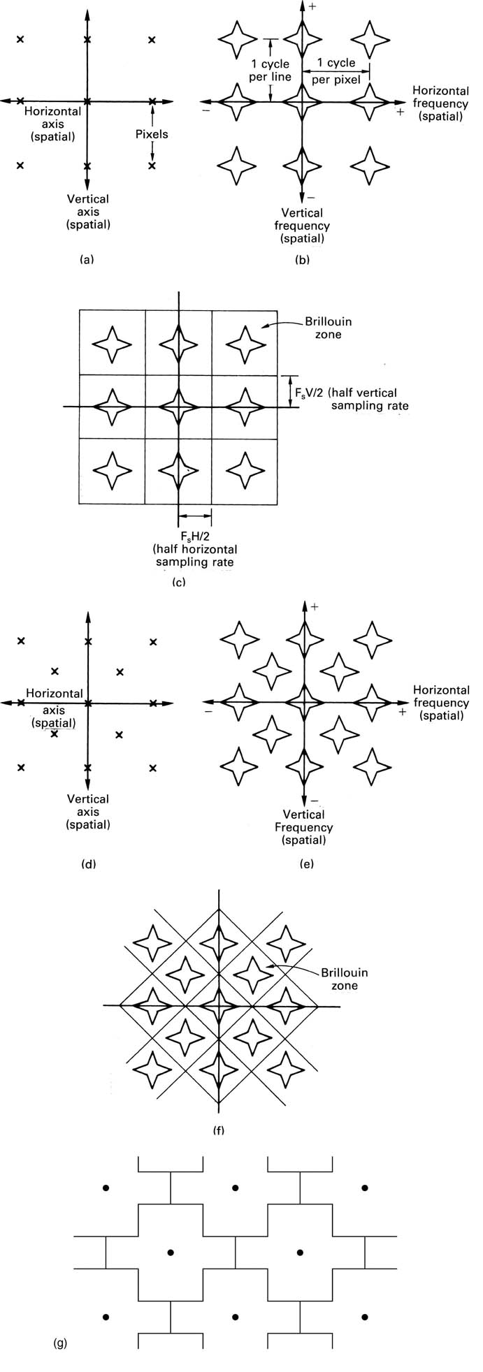
Figure 3.14(a) shows a square matrix of sampling sites which has an identical spatial sampling frequency both vertically and horizontally. The corresponding spectrum is shown in (b). The baseband spectrum is in the centre of the diagram, and the repeating sampling sideband spectrum extends vertically and horizontally. The star-shaped spectrum results from viewing an image of a man-made object such as a building containing primarily horizontal and vertical elements. A more natural scene such as foliage would result in a more circular or elliptical spectrum.
In order to return to the baseband image, the sidebands must be filtered out with a two-dimensional spatial filter. The shape of the two-dimensional frequency response shown in Figure 3.14(c) is known as a Brillouin zone.
Figure 3.14(d) shows an alternative sampling site matrix known as quincunx sampling because of the similarity to the pattern of five dots on a dice. The resultant spectrum has the same characteristic pattern as shown in (e). The corresponding Brillouin zones are shown in (f). Quincunx sampling offers a better compromise between diagonal and horizontal/vertical resolution but is complex to implement.
It is highly desirable to prevent spatial aliasing, since the result is visually irritating. In tube cameras the spatial aliasing will be in the vertical dimension only, since the horizontal dimension is continuously scanned. Such cameras seldom attempt to prevent vertical aliasing. CCD sensors can, however, alias in both horizontal and vertical dimensions, and so an anti-aliasing optical filter is generally fitted between the lens and the sensor. This takes the form of a plate which diffuses the image formed by the lens. Such a device can never have a sharp cut-off nor will the aperture be rectangular. The aperture of the anti-aliasing plate is in series with the aperture effect of the CCD elements, and the combination of the two effectively prevents spatial aliasing, and generally gives a good balance between horizontal and vertical resolution, allowing the picture a natural appearance.
Figure 3.14 Image-sampling spectra. The rectangular array of (a) has a spectrum shown at (b) having a rectangular repeating structure. Filtering to return to the baseband requires a two-dimensional filter whose response lies within the Brillouin zone shown at (c).
Figure 3.14 Quincunx sampling is shown at (d) to have a similar spectral structure (e). An appropriate Brillouin zone is required as at (f). (g) An alternative Brillouin zone for quincunx sampling.
With a conventional approach, there are effectively two choices. If aliasing is permitted, the theoretical information rate of the system can be approached. If aliasing is prevented, realizable anti-aliasing filters cannot sharp cut, and the information conveyed is below system capacity.
These considerations also apply at the television display. The display must filter out spatial frequencies above one half the sampling rate. In a conventional CRT this means that a vertical optical filter should be fitted in front of the screen to render the raster invisible. Again the aperture of a simply realizable filter would attenuate too much of the wanted spectrum, and so the technique is not used.
Figure 3.15 shows the spectrum of analog monochrome video (or of an analog component). The use of interlace has a similar effect on the vertical/temporal spectrum as the use of quincunx sampling on the vertical/horizontal spectrum. The concept of the Brillouin zone cannot really be applied to reconstruction in the spatial/temporal domains. This is because the necessary temporal filtering will be absent in real systems.
Figure 3.15 The vertical/temporal spectrum of monochrome video due to interlace.

3.6 Choice of sampling rate
If the reason for digitizing a video signal is simply to convey it from one place to another, then the choice of sampling frequency can be determined only by sampling theory and available filters. If, however, processing of the video in the digital domain is contemplated, the choice becomes smaller. In order to produce a two-dimensional array of samples which form rows and vertical columns, the sampling rate has to be an integer multiple of the line rate. This allows for the vertical picture processing. Whilst the bandwidth needed by 525/59.94 video is less than that of 625/50, and a lower sampling rate might be used, practicality dictated the choice of a standard sampling rate for video components.
This was the goal of CCIR Recommendation 601, which combined the 625/50 input of EBU Docs Tech. 3246 and 3247 and the 525/59.94 input of SMPTE RP 125. The result is not one sampling rate, but a family of rates based upon the magic frequency of 13.5 MHz. Using this frequency as a sampling rate produces 858 samples in the line period of 525/59.94 and 864 samples in the line period of 625/50. For lower bandwidths, the rate can be divided by three quarters, one half or one quarter to give sampling rates of 10.125, 6.75 and 3.375 MHz respectively. If the lowest frequency is considered to be 1, then the highest is 4. For maximum quality RGB working, then three parallel, identical sample streams would be required, which would be denoted by 4:4:4. Colour difference signals intended for post-production, where a wider colour difference bandwidth is needed, require 4:2:2 sampling for luminance, R-Y and B-Y respectively. 4:2:2 has the advantage that an integer number of colour difference samples also exist in both line standards.
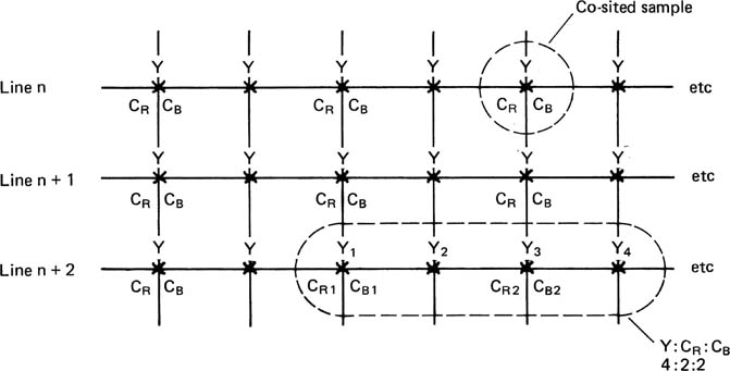
Figure 3.16 shows the spatial arrangement given by 4:2:2 sampling. Luminance samples appear at half the spacing of colour difference samples, and half of the luminance samples are in the same physical position as a pair of colour difference samples, these being called co-sited samples.
Figure 3.16 In CCIR-601 sampling mode 4:2:2, the line synchronous sampling rate of 13.5 MHz results in samples having the same position in successive lines, so that vertical columns are generated. The sampling rates of the colour difference signals CR, CB are one-half of that of luminance, i.e. 6.75 MHz, so that there are alternate Y only samples and co-sited samples which describe Y, CR and CB. In a run of four samples, there will be four Y samples, two CR samples and two CB samples, hence 4:2:2.
Where the signal is likely to be broadcast as PAL or NTSC, a standard of 4:1:1 is acceptable, since this still delivers a colour difference bandwidth in excess of 1 MHz. Where data rate is at a premium, 3:1:1 can be used, and can still offer just about enough bandwidth for 525 lines. This would not be enough for 625-line working, but would be acceptable for ENG applications. The problem with the factors three and one is that they do not offer a columnar sampling structure, and so are not appropriate for processing systems. Figure 3.17(a) shows the one-dimensional spectrum which results from sampling 525/59.94 video at 13.5 MHz, and (b) shows the result for 625/50 video.
Figure 3.17 Spectra of video sampled at 13.5 MHz. In (a) the baseband 525/60 signal at left becomes the sidebands of the sampling rate and its harmonics. In (b) the same process for the 625/50 signal results in a smaller gap between baseband and sideband because of the wider bandwidth of the 625 system. The same sampling rate for both standards results in a great deal of commonality between 50 Hz and 60 Hz equipment.

The traditional TV screen has an aspect ratio of 4:3, whereas digital TV broadcasts have adopted an aspect ratio of 16:9. Expressing 4:3 as 12:9 makes it clear that the 16:9 picture is 16/12 or 4/3 times as wide. There are two ways of handling 16:9 pictures in the digital domain. One is to retain the standard sampling rate of 13.5 MHz, which results in the horizontal resolution falling to 3/4 of its previous value, the other is to increase the sampling rate in proportion to the screen width. This results in a luminance sampling rate of 13.5 x 4/3 MHz or 18.0 MHz.
When composite video is to be digitized, the input will be a single waveform having spectrally interleaved luminance and chroma. Any sampling rate which allows sufficient bandwidth would convey composite video from one point to another, indeed 13.5 MHz has been successfully used to sample PAL and NTSC. However, if simple processing in the digital domain is contemplated, there will be less choice.
In many cases it will be necessary to decode the composite signal which will require some kind of digital filter. Whilst it is possible to construct filters with any desired response, it is a fact that a digital filter whose response is simply related to the sampling rate will be much less complex to implement. This is the reasoning which has led to the near-universal use of four times subcarrier sampling rate.
3.7 Jitter
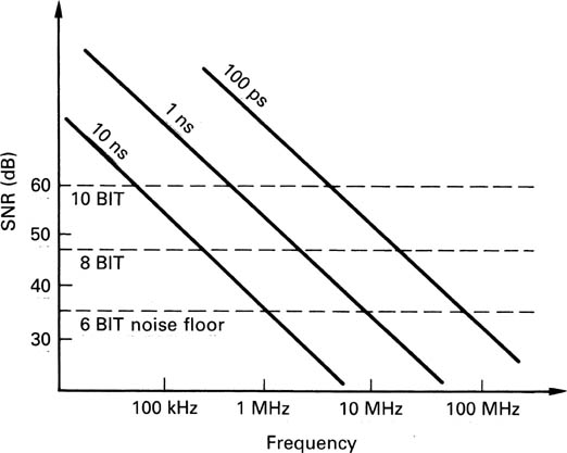
The instants at which samples are taken in an ADC and the instants at which DACs make conversions must be evenly spaced, otherwise unwanted signals can be added to the video. Figure 3.18 shows the effect of sampling clock jitter on a sloping waveform. Samples are taken at the wrong times. When these samples have passed through a system, the timebase correction stage prior to the DAC will remove the jitter, and the result is shown at (b). The magnitude of the unwanted signal is proportional to the slope of the waveform and so the amount of jitter which can be tolerated falls at 6 dB per octave. As the resolution of the system is increased by the use of longer sample wordlength, tolerance to jitter is further reduced. The nature of the unwanted signal depends on the spectrum of the jitter. If the jitter is random, the effect is noise-like and relatively benign unless the amplitude is excessive. Figure 3.19 shows the effect of differing amounts of random jitter with respect to the noise floor of various wordlengths. Note that even small amounts of jitter can degrade a ten-bit convertor to the performance of a good eight-bit unit. There is thus no point in upgrading to higher-resolution convertors if the clock stability of the system is insufficient to allow their performance to be realized.
Figure 3.18 The effect of sampling timing jitter on noise. At (a) a sloping signal sampled with jitter has error proportional to the slope. When jitter is removed by reclocking, the result at (b) is noise.

Figure 3.19 The effect of sampling clock jitter on signal-to-noise ratio at various frequencies, compared with the theoretical noise floors with different wordlengths.
The allowable jitter is measured in picoseconds, and clearly steps must be taken to eliminate it by design. Convertor clocks must be generated from clean power supplies which are well decoupled from the power used by the logic because a convertor clock must have a signal-to-noise ratio of the same order as that of the signal. Otherwise noise on the clock causes jitter which in turn causes noise in the video. The same effect will be found in digital audio signals, which are perhaps more critical.
3.8 Quantizing
Quantizing is the process of expressing some infinitely variable quantity by discrete or stepped values. It turns up in a remarkable number of everyday guises. Figure 3.20 shows that an inclined ramp enables infinitely variable height to be achieved, whereas a step-ladder allows only discrete heights to be had. A stepladder quantizes height. When accountants round off sums of money to the nearest pound or dollar they are quantizing. Time passes continuously, but the display on a digital clock changes suddenly every minute because the clock is quantizing time.
Figure 3.20 An analog parameter is continuous whereas a quantized parameter is restricted to certain values. Here the sloping side of a ramp can be used to obtain any height whereas a ladder only allows discrete heights.

In video and audio the values to be quantized are infinitely variable voltages from an analog source. Strict quantizing is a process which operates in the voltage domain only. For the purpose of studying the quantizing of a single sample, time is assumed to stand still. This is achieved in practice either by the use of a track/hold circuit or the adoption of a quantizer technology such as a flash convertor which operates before the sampling stage.
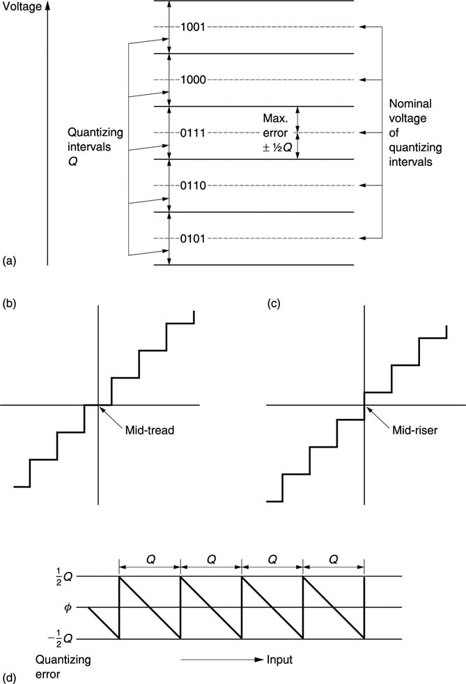
Figure 3.21(a) shows that the process of quantizing divides the voltage range up into quantizing intervals Q, also referred to as steps S. In applications such as telephony these may advantageously be of differing size, but for digital audio the quantizing intervals are made as identical as possible. If this is done, the binary numbers which result are truly proportional to the original analog voltage, and the digital equivalents of mixing and gain changing can be performed by adding and multiplying sample values. If the quantizing intervals are unequal this cannot be done. When all quantizing intervals are the same, the term ‘uniform quantizing’ is used. The term linear quantizing will be found, but this is, like military intelligence, a contradiction in terms.
Figure 3.21 Quantizing assigns discrete numbers to variable voltages. All voltages within the same quantizing interval are assigned the same number which causes a DAC to produce the voltage at the centre of the intervals shown by the dashed lines in (a). This is the characteristic of the mid-tread quantizer shown in (b). An alternative system is the mid-riser system shown in (c). Here 0 Volts analog falls between two codes and there is no code for zero. Such quantizing cannot be used prior to signal processing because the number is no longer proportional to the voltage. Quantizing error cannot exceed ±½Q as shown in (d).
The term LSB (least significant bit) will also be found in place of quantizing interval in some treatments, but this is a poor term because quantizing works in the voltage domain. A bit is not a unit of voltage and can only have two values. In studying quantizing voltages within a quantizing interval will be discussed, but there is no such thing as a fraction of a bit.
Whatever the exact voltage of the input signal, the quantizer will locate the quantizing interval in which it lies. In what may be considered a separate step, the quantizing interval is then allocated a code value which is typically some form of binary number. The information sent is the number of the quantizing interval in which the input voltage lay. Whereabouts that voltage lay within the interval is not conveyed, and this mechanism puts a limit on the accuracy of the quantizer. When the number of the quantizing interval is converted back to the analog domain, it will result in a voltage at the centre of the quantizing interval as this minimizes the magnitude of the error between input and output. The number range is limited by the wordlength of the binary numbers used. In an eight-bit system, 256 different quantizing intervals exist, although in digital video the codes at the extreme ends of the range are reserved for synchronizing.
It is possible to draw a transfer function for such an ideal quantizer followed by an ideal DAC, and this is also shown in Figure 3.21. A transfer function is simply a graph of the output with respect to the input. In electronics, when the term ‘linearity’ is used, this generally means the overall straightness of the transfer function. Linearity is a goal in video and audio convertors, yet it will be seen that an ideal quantizer is anything but linear.
Figure 3.21(b) shows the transfer function is somewhat like a staircase, and blanking level is half-way up a quantizing interval, or on the centre of a tread. This is the so-called mid-tread quantizer which is universally used in video and audio.
Quantizing causes a voltage error in the sample which is given by the difference between the actual staircase transfer function and the ideal straight line. This is shown in Figure 3.21(d) to be a sawtooth-like function which is periodic in Q. The amplitude cannot exceed ±③Q peak-to-peak unless the input is so large that clipping occurs.
Quantizing error can also be studied in the time domain where it is better to avoid complicating matters with the aperture effect of the DAC. For this reason it is assumed here that output samples are of negligible duration. Then impulses from the DAC can be compared with the original analog waveform and the difference will be impulses representing the quantizing error waveform. This has been done in Figure 3.22. The horizontal lines in the drawing are the boundaries between the quantizing intervals, and the curve is the input waveform. The vertical bars are the quantized samples which reach to the centre of the quantizing interval. The quantizing error waveform shown at (b) can be thought of as an unwanted signal which the quantizing process adds to the perfect original. If a very small input signal remains within one quantizing interval, the quantizing error is the signal.
As the transfer function is non-linear, ideal quantizing can cause distortion. As a result, practical digital video equipment deliberately uses non-ideal quantizers to achieve linearity.
As the magnitude of the quantizing error is limited, its effect can be minimized by making the signal larger. This will require more quantizing intervals and more bits to express them. The number of quantizing intervals multiplied by their size gives the quantizing range of the convertor. A signal outside the range will be clipped. Provided that clipping is avoided, the larger the signal, the less will be the effect of the quantizing error.
Where the input signal exercises the whole quantizing range and has a complex waveform (such as from a contrasty, detailed scene), successive samples will have widely varying numerical values and the quantizing error on a given sample will be independent of that on others. In this case the size of the quantizing error will be distributed with equal probability between the limits. Figure 3.22(c)) shows the resultant uniform probability density. In this case the unwanted signal added by quantizing is an additive broadband noise uncorrelated with the signal, and it is appropriate in this case to call it quantizing noise. This is not quite the same as thermal noise which has a Gaussian (bell-shaped) probability shown in Figure 3.22(d). The difference is of no consequence as in the large signal case the noise is masked by the signal. Under these conditions, a meaningful signal-to-noise ratio can be calculated by taking the ratio between the largest signal amplitude which can be accommodated without clipping and the error amplitude. By way of example, an eight-bit system will offer very nearly 50 dB unweighted SNR.
Figure 3.22 In (a) an arbitrary signal is represented to finite accuracy by PAM needles whose peaks are at the centre of the quantizing intervals. The errors caused can be thought of as an unwanted signal (b) added to the original. In (c) the amplitude of a quantizing error needle will be from −③Q to +③Q with equal probability. Note, however, that white noise in analog circuits generally has Gaussian amplitude distribution, shown in (d).

Whilst the above result is true for a large complex input waveform, treatments which then assume that quantizing error is always noise give results which are at variance with reality. The expression above is only valid if the probability density of the quantizing error is uniform. Unfortunately at low depths of modulations, and particularly with flat fields or simple pictures, this is not the case.
At low modulation depth, quantizing error ceases to be random, and becomes a function of the input waveform and the quantizing structure as Figure 3.22 shows. Once an unwanted signal becomes a deterministic function of the wanted signal, it has to be classed as a distortion rather than a noise. Distortion can also be predicted from the non-linearity, or staircase nature, of the transfer function. With a large signal, there are so many steps involved that we must stand well back, and a staircase with 256 steps appears to be a slope. With a small signal there are few steps and they can no longer be ignored.
The effect can be visualized readily by considering a television camera viewing a uniformly painted wall. The geometry of the lighting and the coverage of the lens means that the brightness is not absolutely uniform, but falls slightly at the ends of the TV lines. After quantizing, the gently sloping waveform is replaced by one which stays at a constant quantizing level for many sampling periods and then suddenly jumps to the next quantizing level. The picture then consists of areas of constant brightness with steps between, resembling nothing more than a contour map, hence the use of the term contouring to describe the effect.
Needless to say, the occurrence of contouring precludes the use of an ideal quantizer for high-quality work. There is little point in studying the adverse effects further as they should be and can be eliminated completely in practical equipment by the use of dither. The importance of correctly dithering a quantizer cannot be emphasized enough, since failure to dither irrevocably distorts the converted signal: there can be no process which will subsequently remove that distortion.
3.9 Introduction to dither
At high signal levels, quantizing error is effectively noise. As the depth of modulation falls, the quantizing error of an ideal quantizer becomes more strongly correlated with the signal and the result is distortion, visible as contouring. If the quantizing error can be decorrelated from the input in some way, the system can remain linear but noisy. Dither performs the job of decorrelation by making the action of the quantizer unpredictable and gives the system a noise floor like an analog system.8, 9
All practical digital video systems use non-subtractive dither where the dither signal is added prior to quantization and no attempt is made to remove it at the DAC.10 The introduction of dither prior to a conventional quantizer inevitably causes a slight reduction in the signal-to-noise ratio attainable, but this reduction is a small price to pay for the elimination of non-linearities.
The ideal (noiseless) quantizer of Figure 3.21 has fixed quantizing intervals and must always produce the same quantizing error from the same signal. In Figure 3.23 it can be seen that an ideal quantizer can be dithered by linearly adding a controlled level of noise either to the input signal or to the reference voltage which is used to derive the quantizing intervals. There are several ways of considering how dither works, all of which are equally valid.
Figure 3.23 Dither can be applied to a quantizer in one of two ways. In (a) the dither is linearly added to the analog input signal, whereas in (b) it is added to the reference voltages of the quantizer.

The addition of dither means that successive samples effectively find the quantizing intervals in different places on the voltage scale. The quantizing error becomes a function of the dither, rather than a predictable function of the input signal. The quantizing error is not eliminated, but the subjectively unacceptable distortion is converted into a broadband noise which is more benign to the viewer.
Some alternative ways of looking at dither are shown in Figure 3.24. Consider the situation where a low-level input signal is changing slowly within a quantizing interval. Without dither, the same numerical code is output for a number of sample periods, and the variations within the interval are lost. Dither has the effect of forcing the quantizer to switch between two or more states. The higher the voltage of the input signal within a given interval, the more probable it becomes that the output code will take on the next higher value. The lower the input voltage within the interval, the more probable it is that the output code will take the next lower value. The dither has resulted in a form of duty cycle modulation, and the resolution of the system has been extended indefinitely instead of being limited by the size of the steps.
Figure 3.24 Wideband dither of the appropriate level linearizes the transfer function to produce noise instead of distortion. This can be confirmed by spectral analysis. In the voltage domain, dither causes frequent switching between codes and preserves resolution in the duty cycle of the switching.

Dither can also be understood by considering what it does to the transfer function of the quantizer. This is normally a perfect staircase, but in the presence of dither it is smeared horizontally until with a certain amplitude the average transfer function becomes straight.
3.10 Requantizing and digital dither
Recent ADC technology allows the resolution of video samples to be raised from eight bits to ten or even twelve bits. The situation then arises that an existing eight-bit device such as a digital VTR needs to be connected to the output of an ADC with greater wordlength. The words need to be shortened in some way.
When a sample value is attenuated, the extra low-order bits which come into existence below the radix point preserve the resolution of the signal and the dither in the least significant bit(s) which linearizes the system. The same word extension will occur in any process involving multiplication, such as digital filtering. It will subsequently be necessary to shorten the wordlength. Low-order bits must be removed in order to reduce the resolution whilst keeping the signal magnitude the same. Even if the original conversion was correctly dithered, the random element in the low-order bits will now be some way below the end of the intended word. If the word is simply truncated by discarding the unwanted low-order bits or rounded to the nearest integer the linearizing effect of the original dither will be lost.
Shortening the wordlength of a sample reduces the number of quantizing intervals available without changing the signal amplitude. As Figure 3.25 shows, the quantizing intervals become larger and the original signal is requantized with the new interval structure. This will introduce requantizing distortion having the same characteristics as quantizing distortion in an ADC. It then is obvious that when shortening the wordlength of a ten-bit convertor to eight bits, the two low-order bits must be removed in a way that displays the same overall quantizing structure as if the original convertor had been only of eight-bit wordlength. It will be seen from Figure 3.25 that truncation cannot be used because it does not meet the above requirement but results in signal-dependent offsets because it always rounds in the same direction. Proper numerical rounding is essential in video applications because it accurately simulates analog quantizing to the new interval size. Unfortunately the ten-bit convertor will have a dither amplitude appropriate to quantizing intervals one quarter the size of an eight-bit unit and the result will be highly non-linear.
Figure 3.25 Shortening the wordlength of a sample reduces the number of codes which can describe the voltage of the waveform. This makes the quantizing steps bigger hence the term ‘requantizing’. It can be seen that simple truncation or omission of the bits does not give analogous behaviour. Rounding is necessary to give the same result as if the larger steps had been used in the original conversion.

In practice, the wordlength of samples must be shortened in such a way that the requantizing error is converted to noise rather than distortion. One technique which meets this requirement is to use digital dithering11 prior to rounding. This is directly equivalent to the analog dithering in an ADC.
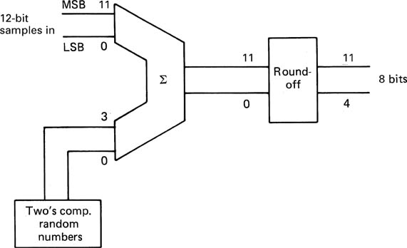
Digital dither is a pseudo-random sequence of numbers. If it is required to simulate the analog dither signal of Figures 3.23 and 3.24, then it is obvious that the noise must be bipolar so that it can have an average voltage of zero. Two’s complement coding must be used for the dither values.
Figure 3.26 shows a simple digital dithering system (i.e. one without noise shaping) for shortening sample wordlength. The output of a two’s complement pseudo-random sequence generator (see Chapter 2) of appropriate wordlength is added to input samples prior to rounding. The most significant of the bits to be discarded is examined in order to determine whether the bits to be removed sum to more or less than half a quantizing interval. The dithered sample is either rounded down, i.e. the unwanted bits are simply discarded, or rounded up, i.e. the unwanted bits are discarded but one is added to the value of the new short word. The rounding process is no longer deterministic because of the added dither which provides a linearizing random component.
Figure 3.26 In a simple digital dithering system, two’s complement values from a random number generator are added to low-order bits of the input. The dithered values are then rounded up or down according to the value of the bits to be removed. The dither linearizes the requantizing.
If this process is compared with that of Figure 3.23 it will be seen that the principles of analog and digital dither are identical; the processes simply take place in different domains using two’s complement numbers which are rounded or voltages that are quantized as appropriate. In fact quantization of an analog dithered waveform is identical to the hypothetical case of rounding after bipolar digital dither where the number of bits to be removed is infinite, and remains identical for practical purposes when as few as eight bits are to be removed. Analog dither may actually be generated from bipolar digital dither (which is no more than random numbers with certain properties) using a DAC.
3.11 Basic digital-to-analog conversion
This direction of conversion will be discussed first, since ADCs often use embedded DACs in feedback loops.
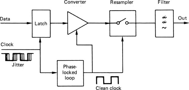
The purpose of a digital-to-analog convertor is to take numerical values and reproduce the continuous waveform that they represent. Figure 3.27 shows the major elements of a conventional conversion subsystem, i.e. one in which oversampling is not employed. The jitter in the clock needs to be removed with a VCO or VCXO. Sample values are buffered in a latch and fed to the convertor element which operates on each cycle of the clean clock. The output is then a voltage proportional to the number for at least a part of the sample period. A resampling stage may be found next, in order to remove switching transients, reduce the aperture ratio or allow the use of a convertor which takes a substantial part of the sample period to operate. The resampled waveform is then presented to a reconstruction filter which rejects frequencies above the audio band.
Figure 3.27 The components of a conventional convertor. A jitter-free clock drives the voltage conversion, whose output may be resampled prior to reconstruction.
This section is primarily concerned with the implementation of the convertor element. The most common way of achieving this conversion is to control binary-weighted currents and sum them in a virtual earth. Figure 3.28 shows the classical R-2R DAC structure. This is relatively simple to construct, but the resistors have to be extremely accurate. To see why this is so, consider the example of Figure 3.29. At (a) the binary code is about to have a major overflow, and all the low-order currents are flowing. At (b), the binary input has increased by one, and only the most significant current flows. This current must equal the sum of all the others plus one. The accuracy must be such that the step size is within the required limits. In this eight-bit example, if the step size needs to be a rather casual 10 per cent accurate, the necessary accuracy is only one part in 2560, but for a ten-bit system it would become one part in 10240. This degree of accuracy is difficult to achieve and maintain in the presence of ageing and temperature change.
Figure 3.28 The classical R-2R DAC requires precise resistance values and ‘perfect’ switches.
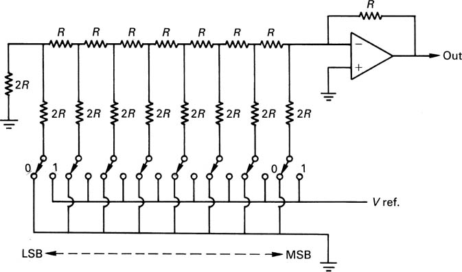
Figure 3.29 At (a) current flow with an input of 0111 is shown. At (b) current flow with input code one greater.

3.12 Basic analog-to-digital conversion
The general principle of a quantizer is that different quantized voltages are compared with the unknown analog input until the closest quantized voltage is found. The code corresponding to this becomes the output. The comparisons can be made in turn with the minimal amount of hardware, or simultaneously with more hardware.
The flash convertor is probably the simplest technique available for PCM video conversion. The principle is shown in Figure 3.30. The threshold voltage of every quantizing interval is provided by a resistor chain which is fed by a reference voltage. This reference voltage can be varied to determine the sensitivity of the input. There is one voltage comparator connected to every reference voltage, and the other input of all the comparators is connected to the analog input. A comparator can be considered to be a one-bit ADC. The input voltage determines how many of the comparators will have a true output. As one comparator is necessary for each quantizing interval, then, for example, in an eight-bit system there will be 255 binary comparator outputs, and it is necessary to use a priority encoder to convert these to a binary code.
The quantizing stage is asynchronous; comparators change state as and when the variations in the input waveform result in a reference voltage being crossed. Sampling takes place when the comparator outputs are clocked into a subsequent latch. This is an example of quantizing before sampling as was illustrated in Figure 3.1. Although the device is simple in principle, it contains a lot of circuitry and can only be practicably implemented on a chip. The analog signal has to drive many inputs which results in a significant parallel capacitance, and a low-impedance driver is essential to avoid restricting the slewing rate of the input. The extreme speed of a flash convertor is a distinct advantage in oversampling. Because computation of all bits is performed simultaneously, no track/hold circuit is required, and droop is eliminated. Figure 3.30(c) shows a flash convertor chip. Note the resistor ladder and the comparators followed by the priority encoder. The MSB can be selectively inverted so that the device can be used either in offset binary or two’s complement mode.
Figure 3.30 The flash convertor. In (a) each quantizing interval has its own comparator, resulting in waveforms of (b). A priority encoder is necessary to convert the comparator outputs to a binary code. Shown in (c) is a typical eight-bit flash convertor primarily intended for video applications. (Courtesy TRW).

3.13 Oversampling
Oversampling means using a sampling rate which is greater (generally substantially greater) than the Nyquist rate. Neither sampling theory nor quantizing theory require oversampling to be used to obtain a given signal quality, but Nyquist rate conversion places extremely high demands on component accuracy when a convertor is implemented. Oversampling allows a given signal quality to be reached without requiring very close tolerance, and therefore expensive, components.
Figure 3.31 shows the main advantages of oversampling. At (a) it will be seen that the use of a sampling rate considerably above the Nyquist rate allows the anti-aliasing and reconstruction filters to be realized with a much more gentle cut-off slope. There is then less likelihood of phase linearity and ripple problems in the passband.
Figure 3.31 Oversampling has a number of advantages. In (a) it allows the slope of analog filters to be relaxed. In (b) it allows the resolution of convertors to be extended. In (c) a noise-shaped convertor allows a disproportionate improvement in resolution.

Figure 3.31(b) shows that information in an analog signal is two-dimensional and can be depicted as an area which is the product of bandwidth and the linearly expressed signal-to-noise ratio. The figure also shows that the same amount of information can be conveyed down a channel with a SNR of half as much (6 dB less) if the bandwidth used is doubled, with 12 dB less SNR if bandwidth is quadrupled, and so on, provided that the modulation scheme used is perfect.
The information in an analog signal can be conveyed using some analog modulation scheme in any combination of bandwidth and SNR which yields the appropriate channel capacity. If bandwidth is replaced by sampling rate and SNR is replaced by a function of wordlength, the same must be true for a digital signal as it is no more than a numerical analog. Thus raising the sampling rate potentially allows the wordlength of each sample to be reduced without information loss.
Information theory predicts that if a signal is spread over a much wider bandwidth by some modulation technique, the SNR of the demodulated signal can be higher than that of the channel it passes through, and this is also the case in digital systems. The concept is illustrated in Figure 3.32. At (a) four-bit samples are delivered at sampling rate F. As four bits have sixteen combinations, the information rate is 16 F. At (b) the same information rate is obtained with three-bit samples by raising the sampling rate to 2 F and at (c) two-bit samples having four combinations require to be delivered at a rate of 4 F. Whilst the information rate has been maintained, it will be noticed that the bit-rate of (c) is twice that of (a). The reason for this is shown in Figure 3.33. A single binary digit can only have two states; thus it can only convey two pieces of information, perhaps ‘yes’ or ‘no’. Two binary digits together can have four states, and can thus convey four pieces of information, perhaps ‘spring summer autumn or winter’, which is two pieces of information per bit. Three binary digits grouped together can have eight combinations, and convey eight pieces of information, perhaps ‘doh re mi fah so lah te or doh’, which is nearly three pieces of information per digit. Clearly the further this principle is taken, the greater the benefit. In a sixteen-bit system, each bit is worth 4K pieces of information. It is always more efficient, in information-capacity terms, to use the combinations of long binary words than to send single bits for every piece of information. The greatest efficiency is reached when the longest words are sent at the slowest rate which must be the Nyquist rate. This is one reason why PCM recording is more common than delta modulation, despite the simplicity of implementation of the latter type of convertor. PCM simply makes more efficient use of the capacity of the binary channel.
Figure 3.32 Information rate can be held constant when frequency doubles by removing one bit from each word. In all cases here it is 16F. Note bit rate of (c) is double that of (a). Data storage in oversampled form is inefficient.

Figure 3.33 The amount of information per bit increases disproportionately as wordlength increases. It is always more efficient to use the longest words possible at the lowest word rate. It will be evident that sixteen-bit PCM is 2048 times as efficient as delta modulation. Oversampled data are also inefficient for storage.

As a result, oversampling is confined to convertor technology where it gives specific advantages in implementation. The storage or transmission system will usually employ PCM, where the sampling rate is a little more than twice the input bandwidth. Figure 3.34 shows a digital VTR using oversampling convertors. The ADC runs at n times the Nyquist rate, but once in the digital domain the rate needs to be reduced in a type of digital filter called a decimator. The output of this is conventional Nyquist rate PCM, according to the tape format, which is then recorded. On replay the sampling rate is raised once more in a further type of digital filter called an interpolator. The system now has the best of both worlds: using oversampling in the convertors overcomes the shortcomings of analog anti-aliasing and reconstruction filters and the wordlength of the convertor elements is reduced making them easier to construct; the recording is made with Nyquist rate PCM which minimizes tape consumption.
Figure 3.34 An oversampling DVTR. The convertors run faster than sampling theory suggests to ease analog filter design. Sampling-rate reduction allows efficient PCM recording on tape.

Oversampling is a method of overcoming practical implementation problems by replacing a single critical element or bottleneck by a number of elements whose overall performance is what counts. As Hauser12 properly observed, oversampling tends to overlap the operations which are quite distinct in a conventional convertor. In earlier sections of this chapter, the vital subjects of filtering, sampling, quantizing and dither have been treated almost independently. Figure 3.35(a) shows that it is possible to construct an ADC of predictable performance by taking a suitable anti-aliasing filter, a sampler, a dither source and a quantizer and assembling them like building bricks. The bricks are effectively in series and so the performance of each stage can only limit the overall performance. In contrast, Figure 3.35(b) shows that with oversampling the overlap of operations allows different processes to augment one another allowing a synergy which is absent in the conventional approach.
Figure 3.35 A conventional ADC performs each step in an identifiable location as in (a). With oversampling, many of the steps are distributed as shown in (b).
If the oversampling factor is n, the analog input must be bandwidth limited to n.Fs/2 by the analog anti-aliasing filter. This unit need only have flat frequency response and phase linearity within the audio band. Analog dither of an amplitude compatible with the quantizing interval size is added prior to sampling at n.Fs and quantizing.
Next, the anti-aliasing function is completed in the digital domain by a low-pass filter which cuts off at Fs/2. Using an appropriate architecture this filter can be absolutely phase linear and implemented to arbitrary accuracy. The filter can be considered to be the demodulator of Figure 3.31 where the SNR improves as the bandwidth is reduced. The wordlength can be expected to increase. The multiplications taking place within the filter extend the wordlength considerably more than the bandwidth reduction alone would indicate. The analog filter serves only to prevent aliasing into the baseband at the oversampling rate; the signal spectrum is determined with greater precision by the digital filter.
With the information spectrum now Nyquist limited, the sampling process is completed when the rate is reduced in the decimator. One sample in n is retained. The excess wordlength extension due to the anti-aliasing filter arithmetic must then be removed. Digital dither is added, completing the dither process, and the quantizing process is completed by requantizing the dithered samples to the appropriate wordlength which will be greater than the wordlength of the first quantizer. Alternatively noise shaping may be employed.
Figure 3.36(a) shows the building-brick approach of a conventional DAC. The Nyquist rate samples are converted to analog voltages and then a steep-cut analog low-pass filter is needed to reject the sidebands of the sampled spectrum. Figure 3.36(b) shows the oversampling approach. The sampling rate is raised in an interpolator which contains a low-pass filter that restricts the baseband spectrum to the audio bandwidth shown. A large frequency gap now exists between the baseband and the lower sideband. The multiplications in the interpolator extend the wordlength considerably and this must be reduced within the capacity of the DAC element by the addition of digital dither prior to requantizing.
Figure 3.36 A conventional DAC in (a) is compared with the oversampling implementation in (b).

Oversampling may also be used to considerable benefit in other dimensions. Figure 3.37 shows how spatial oversampling can be used to increase the resolution of an imaging system. Assuming a 720 × 400 pixel system, Figure 3.37(a) shows that aperture effect would result in an early roll-off of the MTF. Instead a 1440 × 800 pixel sensor is used, having a response shown at (b). This outputs four times as much data, but if these data are passed into a two-dimensional low-pass filter which decimates by a factor of two in each axis, the original bit rate will be obtained once more. This will be a digital filter which can have arbitrarily accurate peformance, including a flat passband and steep cut-off slope. The combination of the aperture effect of the 1440 × 800 pixel camera and the LPF gives a spatial frequency response which is shown in (c). This is better than could be achieved with a 720 × 400 camera. The improvement in subjective quality is quite noticeable in practice.
Figure 3.37 Using an HDTV camera with downconversion is a form of oversampling and gives better results than a normal camera because the aperture effect is overcome.

Oversampling can also be used in the time domain in order to reduce or eliminate display flicker. A different type of standards convertor is necessary which doubles the input field rate by interpolation. The standards convertor must use motion compensation otherwise moving objects will not be correctly positioned in intermediate fields and will suffer from judder. Motion compensation is considered in Chapter 4.
3.14 Gamma in the digital domain
As was explained in section 2.2, the use of gamma makes the transfer function between luminance and the analog video voltage non-linear. This is done because the eye is more sensitive to noise at low brightness. The use of gamma allows the receiver to compress the video signal at low brightness and with it any transmission noise. In the digital domain transmission noise is eliminated, but instead the conversion process introduces quantizing noise. Consequently gamma is retained in the digital domain.
Figure 3.38 shows that digital luma can be considered in several equivalent ways. At (a) a linear analog luminance signal is passed through a gamma corrector to create luma and this is then quantized uniformly. At (b) the linear analog luminance signal is fed directly to a non-uniform quantizer. At (c) the linear analog luminance signal is uniformly quantized to produce digital luminance. This is converted to digital luma by a digital process having a nonlinear transfer function.
Figure 3.38 (a) Analog _γ correction prior to ADC. (b) Non-uniform quantizer gives direct γ conversion. (c) Digital γ correction using look-up table
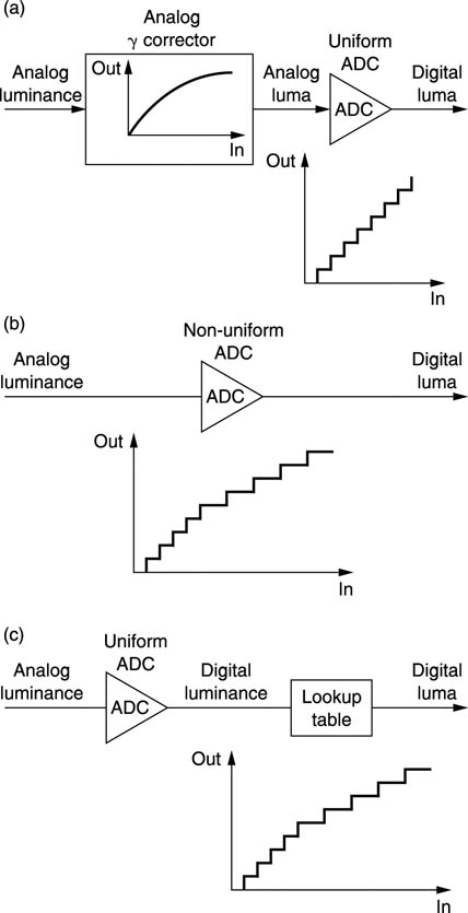
Whilst the three techniques shown give the same result, (a) is the simplest, (b) requires a special ADC with gamma spaced quantizing steps, and (c) requires a high-resolution ADC of perhaps fourteen to sixteen bits because it works in the linear luminance domain where noise is highly visible. Technique (c) is used in digital processing cameras where long wordlength is common practice.
As digital luma with eight-bit resolution gives the same subjective performace as digital luminance with fourteen-bit resolution it will be seen that gamma can also be considered to be an effective perceptive compression technique.
3.15 Colour in the digital domain
Colour cameras and most graphics computers produce three signals, or components, R, G and B which are essentially monochrome video signals representing an image in each primary colour. Figure 3.39 shows that the three primaries are spaced apart in the chromaticity diagram and the only colours which can be generated fall within the resultant triangle.
Figure 3.39 Additive mixing colour systems can only reproduce colours within a triangle where the primaries lie on each vertex.

RGB signals are only strictly compatible if the colour primaries assumed in the source are present in the display. If there is a primary difference the reproduced colours are different. Clearly, broadcast television must have a standard set of primaries. The EBU television systems have only ever had one set of primaries. NTSC began with one set and then adopted another because the phosphors were brighter. Computer displays have any number of standards because initially all computer colour was false. Now that computer displays are going to be used for television it will be necessary for them to adopt standard phosphors or to use colorimetric transcoding on the signals.
Fortunately the human visual system is quite accommodating. The colour of daylight changes throughout the day, so everything changes colour with it. Humans, however, accommodate to that. We tend to see the colour we expect rather than the actual colour. The colour reproduction of printing and photographic media is pretty appalling, but so is human colour memory, and so it’s acceptable.
On the other hand, our ability to discriminate between colours presented simultaneously is razor-sharp, hence the difficulty car repairers have in getting paint to match.
RGB and Y signals are incompatible, yet when colour television was introduced it was a practical necessity that it should be possible to display colour signals on a monochrome display and vice versa.
Creating or transcoding a luma signal from RGB is relatively easy. The spectral response of the eye has a peak in the green region. Green objects will produce a larger stimulus than red objects of the same brightness, with blue objects producing the least stimulus. A luma signal can be obtained by adding R, G and B together, not in equal amounts, but in a sum which is weighted by the relative response of the human visual system. Thus:
Note that the factors add up to one. If Y is derived in this way, a monochrome display will show nearly the same result as if a monochrome camera had been used in the first place. The results are not identical because of the non-linearities introduced by gamma correction.
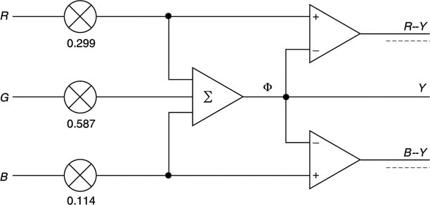
As colour pictures require three signals, it is possible to send Y along with two colour difference signals. There are three possible colour difference signals, R–Y, B–Y and G–Y. As the green signal makes the greatest contribution to Y, then the amplitude of G–Y would be the smallest and would be most susceptible to noise. Thus R–Y and B–Y are used in practice as Figure 3.40 shows. In the digital domain R–Y is known as Cr and B–Y is known as Cb.
Figure 3.40 Colour components are converted to colour difference signals by the transcoding shown here.
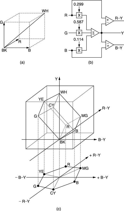
Whilst signals such as Y, R, G and B are unipolar or positive only, colour difference signals are bipolar and may meaningfully take on negative values. Figure 3.41(a) shows the colour space available in eight-bit RGB.
Figure 3.41(c) shows the RGB cube mapped into eight-bit colour difference space so that it is no longer a cube. Now the grey axis goes straight up the middle because greys correspond to both Cr and Cb being zero. To visualize colour difference space, imagine looking down along the grey axis. This makes the black and white corners coincide in the centre. The remaining six corners of the legal colour difference space now correspond to the six boxes on a component vectorscope. Although there are still 16 million combinations, many of these are now illegal. For example, as black or white are approached, the colour differences must fall to zero.
Figure 3.41 RGB transformed to colour difference space. This is done because R-Y and B-Y can be sent with reduced bandwidth. (a) RGB cube. WH-BK axis is diagonal. All locations within cube are legal, (b) RGB to colour difference transform. (c) RGB cube mapped into colour difference space is no longer a cube. Projection down creates conventional vectorscope display.
From an information theory standpoint, colour difference space is redundant. With some tedious geometry, it can be shown that less than a quarter of the codes are legal. The luminance resolution remains the same, but there is about half as much information in each colour axis. This due to the colour difference signals being bipolar. If the signal resolution has to be maintained, eight-bit RGB should be transformed to a longer wordlength in the colour difference domain, nine bits being adequate. At this stage the colour difference transform doesn’t seem efficient because twenty-four-bit RGB converts to twenty-six-bit Y, Cr, Cb.
In most cases the loss of colour resolution is invisible to the eye, and eight-bit resolution is retained. The results of the transform computation must be digitally dithered to avoid posterizing.
The inverse transform to obtain RGB again at the display is straightforward. R and B are readily obtained by adding Y to the two colour difference signals. G is obtained by rearranging the expression for Y above such that:

If a monochrome source having only a Y output is supplied to a colour display, Cr and Cb will be zero. It is reasonably obvious that if there are no colour difference signals the colour signals cannot be different from one another and R = G = B. As a result the colour display can produce only a neutral picture.
The use of colour difference signals is essential for compatibility in both directions between colour and monochrome, but it has a further advantage that follows from the way in which the eye works. In order to produce the highest resolution in the fovea, the eye will use signals from all types of cone, regardless of colour. In order to determine colour the stimuli from three cones must be compared.
There is evidence that the nervous system uses some form of colour difference processing to make this possible. As a result the full acuity of the human eye is available only in monochrome. Detail in colour changes cannot be resolved so well. A further factor is that the lens in the human eye is not achromatic and this means that the ends of the spectrum are not well focused. This is particularly noticeable on blue.
In this case there is no point is expending valuable bandwidth sending highresolution colour signals. Colour difference working allows the luminance to be sent separately at full bandwidth. This determines the subjective sharpness of the picture. The colour difference information can be sent with considerably reduced resolution, as little as one quarter that of luminance, and the human eye is unable to tell.
The acuity of human vision is axisymmetric. In other words, detail can be resolved equally at all angles. When the human visual system assesses the sharpness of a TV picture, it will measure the quality of the worst axis and the extra information on the better axis is wasted. Consequently the most efficient row-and-column image sampling arrangement is the so-called ‘square pixel’. Now pixels are dimensionless and so this is meaningless. However, it is understood to mean that the horizontal and vertical spacing between pixels is the same. Thus it is the sampling grid which is square, rather than the pixel.
The square pixel is optimal for luminance and also for colour difference signals. Figure 3.42 shows the ideal. The colour sampling is co-sited with the luminance sampling but the colour sample spacing is twice that of luminance. The colour difference signals after matrixing from RGB have to be low-pass filtered in two dimensions prior to downsampling in order to prevent aliasing of HF detail. At the display, the downsampled colour data have to be interpolated in two dimensions to produce colour information in every pixel. In an oversampling display the colour interpolation can be combined with the display upsampling stage.
Figure 3.42 Ideal two-dimensionally downsampled colour-difference system. Colour resolution is half of luma resolution, but the eye cannot tell the difference.

Co-siting the colour and luminance pixels means that the transmitted colour values are displayed unchanged. Only the interpolated values need to be calculated. This minimizes generation loss in the filtering. Downsampling the colour by a factor of two in both axes means that the colour data are reduced to one quarter of their original amount. When viewed by a human this is essentially a lossless process.
References
1.Nyquist, H., Certain topics in telegraph transmission theory. AIEE Trans., 617–644 (1928)
2.Shannon, C.E., A mathematical theory of communication. Bell Syst. Tech. J., 27, 379 (1948)
3.Jerri, A.J., The Shannon sampling theorem its various extensions and applications: a tutorial review. Proc. IEEE, 65, 1565–1596 (1977)
4.Whittaker, E.T., On the functions which are represented by the expansions of the interpolation theory. Proc. R. Soc. Edinburgh, 181–194 (1915)
5.Porat, B., A Course in Digital Signal Processing, New York: John Wiley (1997)
6.Betts, J.A., Signal Processing Modulation and Noise, Chapter 6, Sevenoaks: Hodder and Stoughton (1970)
7.Kell, R., Bedford, A. and Trainer, An experimental television system, Part 2. Proc. IRE, 22, 1246–1265 (1934)
8.Goodall, W. M., Television by pulse code modulation. Bell System Tech. Journal, 30, 33–49 (1951)
9.Roberts, L. G., Picture coding using pseudo-random noise. IRE Trans. Inform. Theory, IT-8, 145–154 (1962)
10.Vanderkooy, J. and Lipshitz, S.P., Resolution below the least significant bit in digital systems with dither. J. Audio Eng. Soc, 32, 106–113 (1984)
11.11.Vanderkooy, J. and Lipshitz, S.P., Digital dither. Presented at 81st Audio Eng. Soc. Conv. (Los Angeles 1986), Preprint 2412 (C-8)
12.Hauser, M.W., Principles of oversampling A/D conversion. J. Audio Eng. Soc., 39, 3–26 (1991)