
Chapter 2
Video principles
2.1 The eye
All television signals ultimately excite some response in the eye and the viewer can only describe the result subjectively. Familiarity with the operation and limitations of the eye is essential to an understanding of television principles.
The simple representation of Figure 2.1 shows that the eyeball is nearly spherical and is swivelled by muscles so that it can track movement. This has a large bearing on the way moving pictures are reproduced. The space between the cornea and the lens is filled with transparent fluid known as aqueous humour. The remainder of the eyeball is filled with a transparent jelly known as vitreous humour. Light enters the cornea, and the the amount of light admitted is controlled by the pupil in the iris. Light entering is involuntarily focused on the retina by the lens in a process called visual accommodation.
Figure 2.1 A simple representation of an eyeball; see text for details.

The retina is responsible for light sensing and contains a number of layers. The surface of the retina is covered with arteries, veins and nerve fibres and light has to penetrate these in order to reach the sensitive layer. This contains two types of discrete receptors known as rods and cones from their shape. The distribution and characteristics of these two receptors are quite different. Rods dominate the periphery of the retina whereas cones dominate a central area known as the fovea outside which their density drops off. Vision using the rods is monochromatic and has poor resolution but remains effective at very low light levels, whereas the cones provide high resolution and colour vision but require more light.
The cones in the fovea are densely packed and directly connected to the nervous system allowing the highest resolution. Resolution then falls off away from the fovea. As a result the eye must move to scan large areas of detail. The image perceived is not just a function of the retinal response, but is also affected by processing of the nerve signals. The overall acuity of the eye can be displayed as a graph of the response plotted against the degree of detail being viewed. Image detail is generally measured in lines per millimetre or cycles per picture height, but this takes no account of the distance from the image to the eye. A better unit for eye resolution is one based upon the subtended angle of detail as this will be independent of distance. Units of cycles per degree are then appropriate. Figure 2.2 shows the response of the eye to static detail. Note that the response to very low frequencies is also attenuated. An extension of this characteristic allows the vision system to ignore the fixed pattern of shadow on the retina due to the nerves and arteries.
Figure 2.2 Response of the eye to different degrees of detail.

The retina does not respond instantly to light, but requires between 0.15 and 0.3 second before the brain perceives an image. The resolution of the eye is primarily a spatio-temporal compromise. The eye is a spatial sampling device; the spacing of the rods and cones on the retina represents a spatial sampling frequency. The measured acuity of the eye exceeds the value calculated from the sample site spacing because a form of oversampling is used.
The eye is in a continuous state of unconscious vibration called saccadic motion. This causes the sampling sites to exist in more than one location, effectively increasing the spatial sampling rate provided there is a temporal filter which is able to integrate the information from the various different positions of the retina.
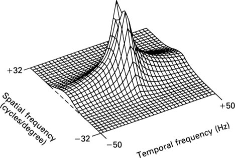
This temporal filtering is responsible for ‘persistence of vision’. Flashing lights are perceived to flicker until the critical flicker frequency (CFF) is reached; the light appears continuous for higher frequencies. The CFF is not constant but varies with brightness. Note that the field rate of European television at 50 fields per second is marginal with bright images. Film projected at 48 Hz works because cinemas are darkened and the screen brightnes is actually quite low. Figure 2.3 shows the two-dimensional or spatio-temporal response of the eye.
Figure 2.3 The response of the eye shown with respect to temporal and spatial frequencies. Note that even slow relative movement causes a serious loss of resolution. The eye tracks moving objects to prevent this loss.
If the eye were static, a detailed object moving past it would give rise to temporal frequencies, as Figure 2.4(a) shows. The temporal frequency is given by the detail in the object, in lines per millimetre, multiplied by the speed. Clearly a highly detailed object can reach high temporal frequencies even at slow speeds, yet Figure 2.3 shows that the eye cannot respond to high temporal frequencies.
Figure 2.4 In (a) a detailed object moves past a fixed eye, causing temporal frequencies beyond the response of the eye. This is the cause of motion blur. In (b) the eye tracks the motion and the temporal frequency becomes zero. Motion blur cannot then occur.
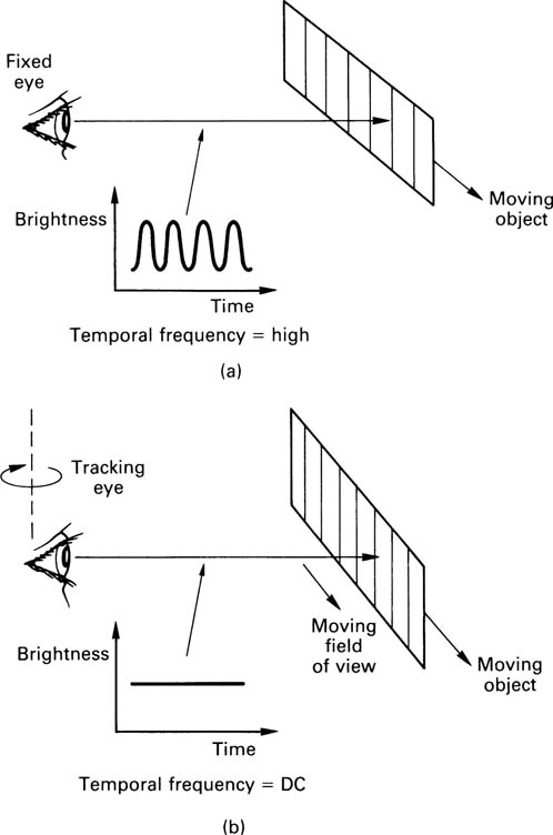
However, the human viewer has an interactive visual system which causes the eyes to track the movement of any object of interest. Figure 2.4(b) shows that when eye tracking is considered, a moving object is rendered stationary with respect to the retina so that temporal frequencies fall to zero and much the same acuity to detail is available despite motion. This is known as dynamic resolution and it’s how humans judge the detail in real moving pictures. Dynamic resolution will be considered in section 2.10.
The contrast sensitivity of the eye is defined as the smallest brightness difference which is visible. In fact the contrast sensitivity is not constant, but increases proportionally to brightness. Thus whatever the brightness of an object, if that brightness changes by about 1 per cent it will be equally detectable.
2.2 Gamma
The true brightness of a television picture can be affected by electrical noise on the video signal. As contrast sensitivity is proportional to brightness, noise is more visible in dark picture areas than in bright areas. For economic reasons, video signals have to be made non-linear to render noise less visible. An inverse gamma function takes place at the camera so that the video signal is non-linear for most of its journey. Figure 2.5 shows a reverse gamma function. As a true power function requires infinite gain near black, a linear segment is substituted. It will be seen that contrast variations near black result in larger signal amplitude than variations near white. The result is that noise picked up by the video signal has less effect on dark areas than on bright areas. After a gamma function at the display, noise at near-black levels is compressed with respect to noise at near-white levels. Thus a video transmission system using gamma has a lower perceived noise level than one without. Without gamma, vision signals would need around 30 dB better signal-to-noise ratio for the same perceived quality and digital video samples would need five or six extra bits.
Figure 2.5 CCIR Rec.709 reverse gamma function used at camera has a straight-line approximation at the lower part of the curve to avoid boosting camera noise. Note that the output amplitude is greater for modulation near black.
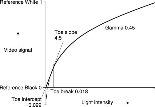
In practice the system is not rendered perfectly linear by gamma correction and a slight overall exponential effect is usually retained in order further to reduce the effect of noise in darker parts of the picture. A gamma correction factor of 0.45 may be used to achieve this effect. Clearly, image data which are intended to be displayed on a video system must have the correct gamma characteristic or the grey scale will not be correctly reproduced.
As all television signals, analog and digital, are subject to gamma correction, it is technically incorrect to refer to the Y signal as luminance, because this parameter is defined as linear in colorimetry. It has been suggested that the term luma should be used to describe luminance which has been gamma corrected.
In a CRT (cathode ray tube) the relationship between the tube drive voltage and the phosphor brightness is not linear, but an exponential function where the power is known as gamma. The power is the same for all CRTs as it is a function of the physics of the electron gun and it has a value of around 2.8. It is a happy but pure coincidence that the gamma function of a CRT follows roughly the same curve as human contrast sensitivity.
Consequently if video signals are predistorted at source by an inverse gamma, the gamma characteristic of the CRT will linearize the signal. Figure 2.6 shows the principle. CRT gamma is not a nuisance, but is actually used to enhance the noise performance of a system. If the CRT had no gamma characteristic, a gamma circuit would have been necessary ahead of it. As all standard video signals are inverse gamma processed, it follows that if a non-CRT display such as a plasma or LCD device is to be used, some gamma conversion will be required at the display.
Figure 2.6 The non-linear characteristic of tube (a) contrasted with the ideal response (b). Non-linearity may be opposed by gamma correction with a response (c).

2.3 Scanning
Figure 2.7(a) shows that the monochrome camera produces a video signal whose voltage is a function of the image brightness at a single point on the sensor. This voltage is converted back to the brightness of the same point on the display. The points on the sensor and display must be scanned synchronously if the picture is to be re-created properly. If this is done rapidly enough it is largely invisible to the eye. Figure 2.7(b) shows that the scanning is controlled by a triangular or sawtooth waveform in each dimension which causes a constant speed forward scan followed by a rapid return or flyback. As the horizontal scan is much more rapid than the vertical scan the image is broken up into lines which are not quite horizontal.
Figure 2.7 Scanning converts two-dimensional images into a signal which can be sent electrically. In (a) the scanning of camera and display must be identical. The scanning is controlled by horizontal and vertical sawtooth waveforms (b). Where two vertical scans are needed to complete a whole number of lines, the scan is interlaced as shown in (c). The frame is now split into two fields.
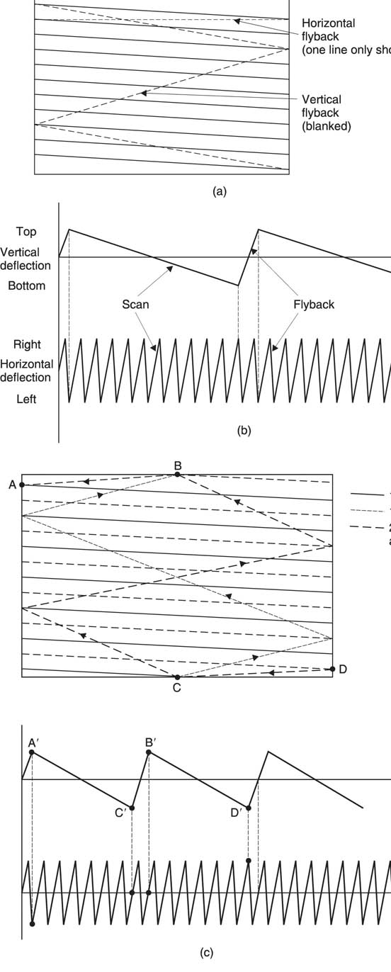
In the example of Figure 2.7(b), the horizontal scanning frequency or line rate, Fh, is an integer multiple of the vertical scanning frequency or frame rate and a progressive scan system results in which every frame is identical. Figure 2.7(c) shows an interlaced scan system in which there is an integer number of lines in two vertical scans or fields. The first field begins with a full line and ends on a half line and the second field begins with a half line and ends with a full line. The lines from the two fields interlace or mesh on the screen. Current analog broadcast systems such as PAL and NTSC use interlace, although in MPEG systems it is not necessary. The additional complication of interlace has both merits and drawbacks which will be discussed in section 2.11.
2.4 Synchronizing
The synchronizing or sync system must send timing information to the display alongside the video signal. In very early television equipment this was achieved using two quite separate or non-composite signals. Figure 2.8(a) shows one of the first (US) television signal standards in which the video waveform had an amplitude of 1 V peak-to-peak and the sync signal had an amplitude of 4 V peakto-peak. In practice, it was more convenient to combine both into a single electrical waveform then called composite video which carries the synchronizing information as well as the scanned brightness signal. The single signal is effectively shared by using some of the flyback period for synchronizing.
Figure 2.8 Early video used separate vision and sync signals shown in (a). The US one volt video waveform in (b) has 10:4 video/sync ratio. (c) European systems use 7:3 ratio to avoid odd voltages. (d) Sync separation relies on two voltage ranges in the signal.

The 4 V sync signal was attenuated by a factor of ten and added to the video to produce a 1.4 V peak-to-peak signal. This was the origin of the 10:4 video:sync relationship of US analog television practice. Later the amplitude was reduced to 1 V peak-to-peak so that the signal had the same range as the original non-composite video. The 10:4 ratio was retained. As Figure 2.8(b) shows, this ratio results in some rather odd voltages and to simplify matters, a new unit called the IRE unit (after the Institute of Radio Engineers) was devised. Originally this was defined as 1 per cent of the video voltage swing, independent of the actual amplitude in use, but it came in practice to mean 1 per cent of 0.714 V. In European analog systems shown in Figure 2.8(c) the messy numbers were avoided by using a 7:3 ratio and the waveforms are always measured in milliVolts. Whilst such a signal was originally called composite video, today it would be referred to as monochrome video or Ys, meaning luma carrying syncs although in practice the s is often omitted.
Figure 2.8(d) shows how the two signals are separated. The voltage swing needed to go from black to peak white is less than the total swing available. In a standard analog video signal the maximum amplitude is 1 V peak-to-peak. The upper part of the voltage range represents the variations in brightness of the image from black to white. Signals below that range are ‘blacker than black’ and cannot be seen on the display. These signals are used for synchronizing.
Figure 2.9(a) shows the line synchronizing system part-way through a field or frame. The part of the waveform which corresponds to the forward scan is called the active line and during the active line the voltage represents the brightness of the image. In between the active line periods are horizontal blanking intervals in which the signal voltage will be at or below black. Figure 2.9(b) shows that in some systems the active line voltage is superimposed on a pedestal or black level set-up voltage of 7.5 IRE. The purpose of this set-up is to ensure that the blanking interval signal is below black on simple displays so that it is guaranteed to be invisible on the screen. When set-up is used, black level and blanking level differ by the pedestal height. When set-up is not used, black level and blanking level are one and the same.
Figure 2.9 (a) Part of a video waveform with important features named. (b) Use of pedestal or set-up.

The blanking period immediately after the active line is known as the front porch, which is followed by the leading edge of sync. When the leading edge of sync passes through 50 per cent of its own amplitude, the horizontal retrace pulse is considered to have occurred. The flat part at the bottom of the horizontal sync pulse is known as sync tip and this is followed by the trailing edge of sync which returns the waveform to blanking level. The signal remains at blanking level during the back porch during which the display completes the horizontal flyback. The sync pulses have sloping edges because if they were square they would contain high frequencies which would go outside the allowable channel bandwidth on being broadcast.
The vertical synchronizing system is more complex because the vertical flyback period is much longer than the horizontal line period and horizontal synchronization must be maintained throughout it. The vertical synchronizing pulses are much longer than horizontal pulses so that they are readily distinguishable. Figure 2.10(a) shows a simple approach to vertical synchronizing. The signal remains predominantly at sync tip for several lines to indicate the vertical retrace, but returns to blanking level briefly immediately prior to the leading edges of the horizontal sync, which continues throughout. Figure 2.10(b) shows that the presence of interlace complicates matters, as in one vertical interval the vertical sync pulse coincides with a horizontal sync pulse whereas in the next the vertical sync pulse occurs half-way down a line.
Figure 2.10 (a) A simple vertical pulse is longer than a horizontal pulse. (b) In an interlaced system there are two relationships between H and V. (c) The use of equalizing pulses to balance the DC component of the signal.

In practice the long vertical sync pulses were found to disturb the average signal voltage too much and to reduce the effect extra equalizing pulses were put in, half-way between the horizontal sync pulses. The horizontal timebase system can ignore the equalizing pulses because it contains a flywheel circuit which only expects pulses roughly one line period apart. Figure 2.10(c) shows the final result of an interlaced system with equalizing pulses. The vertical blanking interval can be seen, with the vertical pulse itself towards the beginning.
In digital video signals it is possible to synchronize simply by digitizing the analog sync pulses. However, this is inefficient because many samples are needed to describe them. In practice the analog sync pulses are used to generate timing reference signals (TRS) which are special codes inserted in the video data which indicate the picture timing. In a manner analogous to the analog approach of dividing the video voltage range into two, one for syncs, the solution in the digital domain is the same: certain bit combinations are reserved for TRS codes and these cannot occur in legal video. TRS codes are detailed in Chapter 9.
It is essential accurately to extract the timing or synchronizing information from a sync or Ys signal in order to control some process such as the generation of a digital sampling clock. Figure 2.11(a) shows a block diagram of a simple sync separator. The first stage will generally consist of a black level clamp which stabilizes the DC conditions in the separator. Figure 2.11(b) shows that if this is not done the presence of a DC shift on a sync edge can cause a timing error.
Figure 2.11 (a) Sync separator block diagram; see text for details. (b) Slicing at the wrong level introduces a timing error. (c) The timing of the sync separation process.
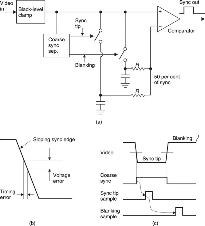
The sync time is defined as the instant when the leading edge passes through the 50 per cent level. The incoming signal should ideally have a sync amplitude of either 0.3 V peak-to-peak or 40 IRE, in which case it can be sliced or converted to a binary waveform by using a comparator with a reference of either 0.15 V or 20 IRE. However, if the sync amplitude is for any reason incorrect, the slicing level will be wrong. Figure 2.11(a) shows that the solution is to measure both blanking and sync tip voltages and to derive the slicing level from them with a potential divider. In this way the slicing level will always be 50 per cent of the input amplitude. In order to measure the sync tip and blanking levels, a coarse sync separator is required, which is accurate enough to generate sampling pulses for the voltage measurement system. Figure 2.11(c) shows the timing of the sampling process.
Once a binary signal has been extracted from the analog input, the horizontal and vertical synchronizing information can be separated. All falling edges are potential horizontal sync leading edges, but some are due to equalizing pulses and these must be rejected. This is easily done because equalizing pulses occur part-way down the line. A flywheel oscillator or phase-locked loop will lock to genuine horizontal sync pulses because they always occur exactly one line period apart. Edges at other spacings are eliminated. Vertical sync is detected with a timer whose period exceeds that of a normal horizontal sync pulse. If the sync waveform is still low when the timer expires, there must be a vertical pulse present. Once again a phase-locked loop may be used which will continue to run if the input is noisy or disturbed. This may take the form of a counter which counts the number of lines in a frame before resetting.
The sync separator can determine which type of field is beginning because in one the vertical and horizontal pulses coincide whereas in the other the vertical pulse begins in the middle of a line.
2.5 Bandwidth and definition
As the conventional analog television picture is made up of lines, the line structure determines the definition or the fineness of detail which can be portrayed in the vertical axis. The limit is reached in theory when alternate lines show black and white. In a 625-line picture there are roughly 600 unblanked lines. If 300 of these are white and 300 are black then there will be 300 complete cycles of detail in one picture height. One unit of resolution, which is a unit of spatial frequency, is c/ph or cycles per picture height. In practical displays the contrast will have fallen to virtually nothing at this ideal limit and the resolution actually achieved is around 70 per cent of the ideal, or about 210 c/ph. The degree to which the ideal is met is known as the Kell factor of the display.
Definition in one axis is wasted unless it is matched in the other and so the horizontal axis should be able to offer the same performance. As the aspect ratio of conventional television is 4:3 then it should be possible to display 400 cycles in one picture width, reduced to about 300 cycles by the Kell factor. As part of the line period is lost due to flyback, 300 cycles per picture width becomes about 360 cycles per line period.
In 625-line television, the frame rate is 25 Hz and so the line rate Fh will be:
If 360 cycles of video waveform must be carried in each line period, then the bandwidth required will be given by:
In the 525-line system, there are roughly 500 unblanked lines allowing 250 c/ph theoretical definition, or 175 lines allowing for the Kell factor. Allowing for the aspect ratio, equal horizontal definition requires about 230 cycles per picture width. Allowing for horizontal blanking this requires about 280 cycles per line period.
In 525-line video, Fh = 525 χ 30 = 15 750 Hz Thus the bandwidth required is:
If it is proposed to build a high-definition television system, one might start by doubling the number of lines and hence double the definition. Thus in a 1250-line format about 420 c/ph might be obtained. To achieve equal horizontal definition, bearing in mind the aspect ratio is now 16:9, then nearly 750 cycles per picture width will be needed. Allowing for horizontal blanking, then around 890 cycles per line period will be needed. The line frequency is now given by:
and the bandwidth required is given by
Note the dramatic increase in bandwidth. In general the bandwidth rises as the square of the resolution because there are more lines and more cycles needed in each line. It should be clear that, except for research purposes, high-definition television will never be broadcast as a conventional analog signal because the bandwidth required is simply uneconomic. If and when high-definition broadcasting becomes common, it will be compelled to use digital compression techniques to make it economic.
2.6 Aperture effect
The aperture effect will show up in many aspects of television in both the sampled and continuous domains. The image sensor has a finite aperture function. In tube cameras and in CRTs, the beam will have a finite radius with a Gaussian distribution of energy across its diameter. This results in a Gaussian spatial frequency response. Tube cameras often contain an aperture corrector which is a filter designed to boost the higher spatial frequencies that are attenuated by the Gaussian response. The horizontal filter is simple enough, but the vertical filter will require line delays in order to produce points above and below the line to be corrected. Aperture correctors also amplify aliasing products and an overcorrected signal may contain more vertical aliasing than resolution.
Some digital-to-analog convertors keep the signal constant for a substantial part of or even the whole sample period. In CCD cameras, the sensor is split into elements which may almost touch in some cases. The element integrates light falling on its surface. In both cases the aperture will be rectangular. The case where the pulses have been extended in width to become equal to the sample period is known as a zero-order hold system and has a 100 per cent aperture ratio.
Rectangular apertures have a sinx/x spectrum which is shown in Figure 2.12. With a 100 per cent aperture ratio, the frequency response falls to a null at the sampling rate, and as a result is about 4 dB down at the edge of the baseband.
Figure 2.12 Frequency response with 100 per cent aperture nulls at multiples of sampling rate. Area of interest is up to half sampling rate.

The temporal aperture effect varies according to the equipment used. Tube cameras have a long integration time and thus a wide temporal aperture. Whilst this reduces temporal aliasing, it causes smear on moving objects. CCD cameras do not suffer from lag and as a result their temporal response is better. Some CCD cameras deliberately have a short temporal aperture as the time axis is resampled by a shutter. The intention is to reduce smear, hence the popularity of such devices for sporting events, but there will be more aliasing on certain subjects.
The eye has a temporal aperture effect which is known as persistence of vision, and the phosphors of CRTs continue to emit light after the electron beam has passed. These produce further temporal aperture effects in series with those in the camera.
2.7 Colour
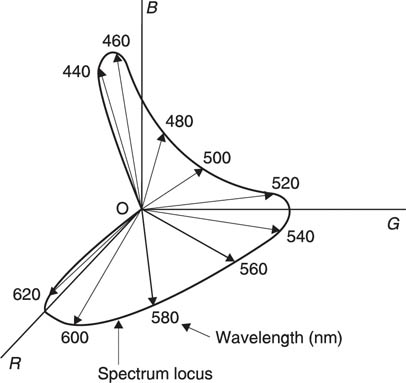
Colour vision is made possible by the cones on the retina which occur in three different types, responding to different colours. Figure 2.13 shows that human vision is restricted to range of light wavelengths from 400 nanometres to 700 nanometres. Shorter wavelengths are called ultra-violet and longer wavelengths are called infra-red. Note that the response is not uniform, but peaks in the area of green. The response to blue is very poor and makes a nonsense of the traditional use of blue lights on emergency vehicles.
Figure 2.13 The luminous efficiency function shows the response of the HVS to light of different wavelengths.

Figure 2.14 shows an approximate response for each of the three types of cone. If light of a single wavelength is observed, the relative responses of the three sensors allows us to discern what we call the colour of the light. Note that at both ends of the visible spectrum there are areas in which only one receptor responds; all colours in those areas look the same. There is a great deal of variation in receptor response from one individual to the next and the curves used in television are the average of a great many tests. In a surprising number of people the single receptor zones are extended and discrimination between, for example, red and orange is difficult.
Figure 2.14 All human vision takes place over this range of wavelengths. The response is not uniform, but has a central peak. The three types of cone approximate to the three responses shown to give colour vision.

The full resolution of human vision is restricted to brightness variations. Our ability to resolve colour details is only about a quarter of that.
The triple receptor characteristic of the eye is extremely fortunate as it means that we can generate a range of colours by adding together light sources having just three different wavelengths in various proportions. This process is known as additive colour matching which should be clearly distinguished from the subtractive colour matching that occurs with paints and inks. Subtractive matching begins with white light and selectively removes parts of the spectrum by filtering. Additive matching uses coloured light sources which are combined.
An effective colour television system can be made in which only three pure or single-wavelength colours or primaries can be generated. The primaries need to be similar in wavelength to the peaks of the three receptor responses, but need not be identical. Figure 2.15 shows a rudimentary colour television system. Note that the colour camera is in fact three cameras in one, where each is fitted with a different coloured filter. Three signals, R, G and B must be transmitted to the display which produces three images that must be superimposed to obtain a colour picture.
Figure 2.15 Simple colour television system. Camera image is split by three filters. Red, green and blue video signals are sent to three primary coloured displays whose images are combined.

In practice the primaries must be selected from available phosphor compounds. Once the primaries have been selected, the proportions needed to reproduce a given colour can be found using a colorimeter. Figure 2.16 shows a colorimeter which consists of two adjacent white screens. One screen is illuminated by three light sources, one of each of the selected primary colours. Initially, the second screen is illuminated with white light and the three sources are adjusted until the first screen displays the same white. The sources are then calibrated. Light of a single wavelength is then projected on the second screen. The primaries are once more adjusted until both screens appear to have the same colour. The proportions of the primaries are noted. This process is repeated for the whole visible spectrum, resulting in colour mixture curves shown in Figure 2.17. In some cases it will not be possible to find a match because an impossible negative contribution is needed. In this case we can simulate a negative contribution by shining some primary colour on the test screen until a match is obtained. If the primaries were ideal, monochromatic or single-wavelength sources, it would be possible to find three wavelengths at which two of the primaries were completely absent. However, practical phosphors are not monochromatic, but produce a distribution of wavelengths around the nominal value, and in order to make them spectrally pure other wavelengths have to be subtracted.
Figure 2.16 Simple colorimeter. Intensities of primaries on the right screen are adjusted to match the test colour on the left screen.
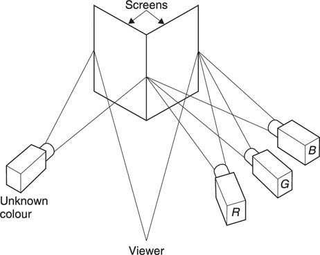
Figure 2.17 Colour mixture curves show how to mix primaries to obtain any spectral colour.

The colour-mixing curves dictate what the response of the three sensors in the colour camera must be. The primaries are determined in this way because it is easier to make camera filters to suit available CRT phosphors rather than the other way round.
As there are three signals in a colour television system, they can only be simultaneously depicted in three dimensions. Figure 2.18 shows the RGB colour space which is basically a cube with black at the origin and white at the diagonally opposite corner. Figure 2.19 shows the colour mixture curves plotted in RGB space. For each visible wavelength a vector exists whose direction is determined by the proportions of the three primaries. If the brightness is allowed to vary this will affect all three primaries and thus the length of the vector in the same proportion.
Figure 2.18 RGB colour space is three-dimensional and not easy to draw.

Figure 2.19 Colour mixture curves plotted in RGB space result in a vector whose locus moves with wavelength in three dimensions.
Depicting and visualizing the RGB colour space is not easy and it is also difficult to take objective measurements from it. The solution is to modify the diagram to allow it to be rendered in two dimensions on flat paper. This is done by eliminating luminance (brightness) changes and depicting only the colour at constant brightness. Figure 2.20(a) shows how a constant luminance unit plane intersects the RGB space at unity on each axis. At any point on the plane the three components add up to one. A two-dimensional plot results when vectors representing all colours intersect the plane. Vectors may be extended if necessary to allow intersection. Figure 2.20(b) shows that the 500 nm vector has to be produced (extended) to meet the unit plane, whereas the 580 nm vector naturally intersects. Any colour can now uniquely be specified in two dimensions.
Figure 2.20 (a) A constant luminance plane intersects RGB space, allowing colours to be studied in two dimensions only. (b) The intersection of the unit plane by vectors joining the origin and the spectrum locus produces the locus of spectral colours which requires negative values of R, G and B to describe it. In (c) a new coordinate system, X, Y, Z, is used so that only positive values are required. The spectrum locus now fits entirely in the triangular space where the unit plane intersects these axes. To obtain the CIE chromaticity diagram (d), the locus is projected onto the X–Y plane.
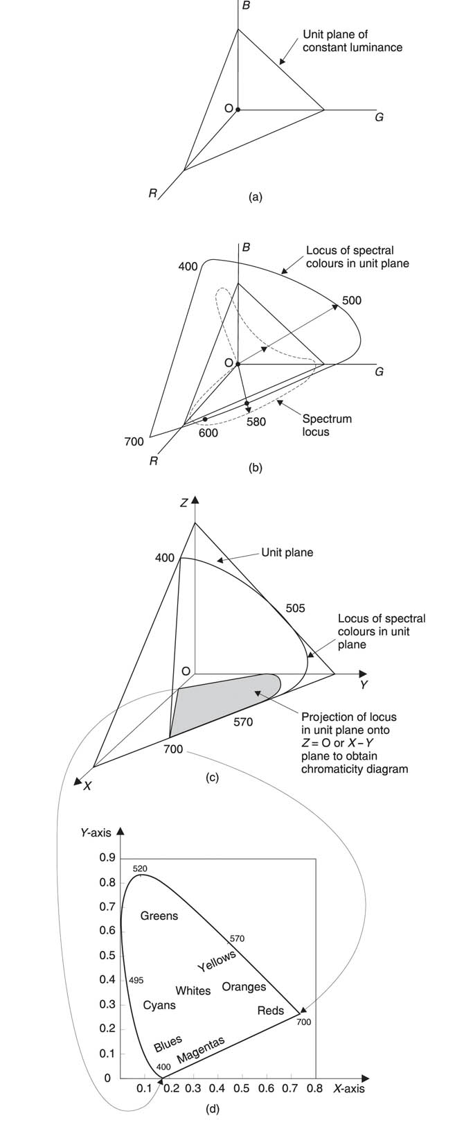
The points where the unit plane intersects the axes of RGB space form a triangle on the plot. The horseshoe-shaped locus of pure spectral colours goes outside this triangle because, as was seen above, the colour mixture curves require negative contributions for certain colours.
Having the spectral locus outside the triangle is a nuisance, and a larger triangle can be created by postulating new coordinates called X, Y and Z representing hypothetical primaries that cannot exist. This representation is shown in Figure 2.20(c).
The Commission Internationale d’Eclairage (CIE) standard chromaticity diagram shown in Figure 2.20(d) is obtained in this way by projecting the unity luminance plane onto the X, Y plane. This projection has the effect of bringing the red and blue primaries closer together. Note that the curved part of the locus is due to spectral or single-wavelength colours. The straight base is due to nonspectral colours obtained by additively mixing red and blue.
As negative light is impossible, only colours within the triangle joining the primaries can be reproduced and so practical television systems cannot reproduce all possible colours. Clearly, efforts should be made to obtain primaries which embrace as large an area as possible. Figure 2.21 shows how the colour range or gamut of television compares with paint and printing inks and illustrates that the comparison is favourable. Most everyday scenes fall within the colour gamut of television. Exceptions include saturated turquoise, spectrally pure iridescent colours formed by interference in a duck’s feathers or reflections in Compact Discs. For special purposes displays have been made having four primaries to give a wider colour range, but these are uncommon.
Figure 2.21 Comparison of the colour range of television and printing.

Figure 2.22 shows the primaries initially selected for NTSC. However, manufacturers looking for brighter displays substituted more efficient phosphors having a smaller colour range. This was later standardized as the SMPTE C phosphors which were also adopted for PAL.
Figure 2.22 The primary colours for NTSC were initially as shown. These were later changed to more efficient phosphors which were also adopted for PAL. See text.

Whites appear in the centre of the chromaticity diagram corresponding to roughly equal amounts of primary colour. Two terms are used to describe colours: hue and saturation. Colours having the same hue lie on a straight line between the white point and the perimeter of the primary triangle. The saturation of the colour increases with distance from the white point. As an example, pink is a desaturated red.
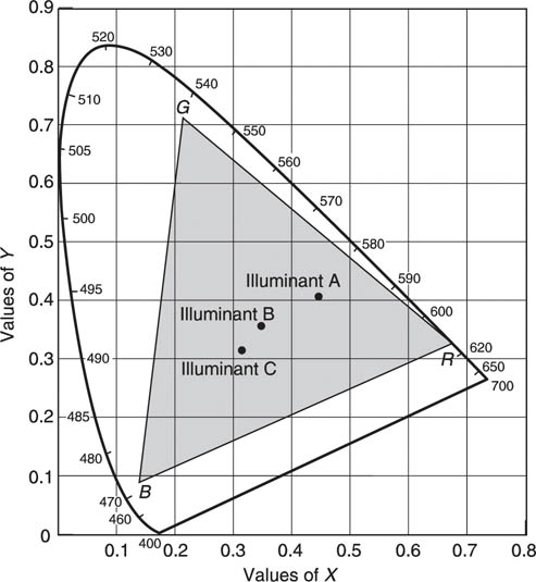
The apparent colour of an object is also a function of the illumination. The ‘true colour’ will only be revealed under ideal white light which in practice is uncommon. An ideal white object reflects all wavelengths equally and simply takes on the colour of the ambient illumination. Figure 2.23 shows the location of three ‘white’ sources or illuminants on the chromaticity diagram. Illuminant A corresponds to a tungsten filament lamp, illuminant B to midday sunlight and illuminant C to typical daylight which is bluer because it consists of a mixture of sunlight and light scattered by the atmosphere. In everyday life we accommodate automatically to the change in apparent colour of objects as the sun’s position or the amount of cloud changes and as we enter artificially lit buildings, but colour cameras accurately reproduce these colour changes. Attempting to edit a television program from recordings made at different times of day or indoors and outdoors would result in obvious and irritating colour changes unless some steps are taken to keep the white balance reasonably constant.
Figure 2.23 Position of three common illuminants on chromaticity diagram.
2.8 Colour displays
In order to display colour pictures, three simultaneous images must be generated, one for each primary colour. The colour CRT does this geometrically. Figure 2.24(a) shows that three electron beams pass down the tube from guns mounted in a triangular or delta array. Immediately before the tube face is mounted a perforated metal plate known as a shadow mask. The three beams approach holes in the shadow mask at a slightly different angle and so fall upon three different areas of phosphor which each produce a different primary colour. The sets of three phosphors are known as triads. Figure 2.24(b) shows an alternative arrangement in which the three electron guns are mounted in a straight line and the shadow mask is slotted and the triads are rectangular. This is known as a PIL (precision-in-line) tube. The triads can easily be seen upon close inspection of an operating CRT.
Figure 2.24 (a) Triads of phosphor dots are triangular and electron guns are arranged in a triangle. (b) Inline tube has strips of phosphor side by side.

In the plasma display the source of light is an electrical discharge in a gas at low pressure. This generates ultra-violet light which excites phosphors in the same way that a fluorescent light operates. Each pixel consists of three such elements, one for each primary colour. Figure 2.25 shows that the pixels are controlled by arranging the discharge to take place between electrodes which are arranged in rows and columns.
Figure 2.25 When a voltage is applied between a line or row electrode and a pixel electrode, a plasma discharge occurs. This excites a phosphor to produce visible light.

The advantage of the plasma display is that it can be made perfectly flat and it is very thin, even in large screen sizes. There is a size limit in CRTs beyond which they become very heavy. Plasma displays allow this limit to be exceeded.
The great difficulty with the plasma display is that the relationship between light output and drive voltage is highly non-linear. Below a certain voltage there is no discharge at all. Consequently the only way that the brightness can be varied is to modulate the time for which the discharge takes place. The electrode signals are pulse width modulated.
Eight-bit digital video has 256 different brightnesses and it is difficult to obtain such a scale by pulse width modulation as the increments of pulse length would need to be generated by a clock of fantastic frequency. It is common practice to break up the picture period into many pulses, each of which is modulated in width. Despite this, plasma displays often display contouring or posterizing, indicating a lack of sufficient brightness levels. Multiple pulse drive also has some temporal effects which may be visible on moving material unless motion compensation is used.
2.9 Colour difference signals
There are many different ways in which television signals can be carried and these will be considered here. A monochrome camera produces a single luma signal Y or Ys whereas a colour camera produces three signals, or components, R, G and B which are essentially monochrome video signals representing an image in each primary colour. In some systems sync is present on a separate signal (RGBS), rarely is it present on all three components, whereas most commonly it is only present on the green component leading to the term RGsB. The use of the green component for sync has led to suggestions that the components should be called GBR. As the original and long-standing term RGB or RGsB correctly reflects the sequence of the colours in the spectrum it remains to be seen whether GBR will achieve common usage. Like luma, RGsB signals may use 0.7 or 0.714 V signals, with or without set-up.
RGB and Y signals are incompatible, yet when colour television was introduced it was a practical necessity that it should be possible to display colour signals on a monochrome display and vice versa.
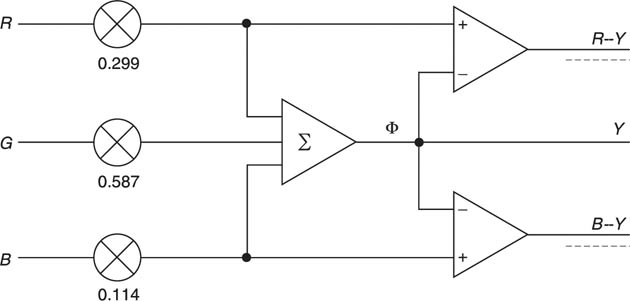
Creating or transcoding a luma signal from R, Gs and B is relatively easy. Figure 2.13 showed the spectral response of the eye which has a peak in the green region. Green objects will produce a larger stimulus than red objects of the same brightness, with blue objects producing the least stimulus. A luma signal can be obtained by adding R, G and B together, not in equal amounts, but in a sum which is weighted by the relative response of the eye. Thus:
Syncs may be regenerated, but will be identical to those on the Gs input and when added to Y result in Ys as required.
If Ys is derived in this way, a monochrome display will show nearly the same result as if a monochrome camera had been used in the first place. The results are not identical because of the non-linearities introduced by gamma correction.
As colour pictures require three signals, it should be possible to send Ys and two other signals which a colour display could arithmetically convert back to R, G and B. There are two important factors which restrict the form which the other two signals may take. One is to achieve reverse compatibility. If the source is a monochrome camera, it can only produce Ys and the other two signals will be completely absent. A colour display should be able to operate on the Ys signal only and show a monochrome picture. The other is the requirement to conserve bandwidth for economic reasons.
These requirements are met by sending two colour difference signals along with Ys. There are three possible colour difference signals, R–Y, B–Y and G. As the green signal makes the greatest contribution to, then the amplitude of G–Y would be the smallest and would be most susceptible to noise. Thus R–Y and B–Y are used in practice as Figure 2.26 shows.
Figure 2.26 Colour components are converted to colour difference signals by the transcoding shown here.
R and B are readily obtained by adding Y to the two colour difference signals. G is obtained by rearranging the expression for Y above such that:

If a colour CRT is being driven, it is possible to apply inverted luma to the cathodes and the R – Y and B – Y signals directly to two of the grids so that the tube performs some of the matrixing. It is then only necessary to obtain G – Y for the third grid, using the expression:
If a monochrome source having only a Ys output is supplied to a colour display, R–Y and B–Y will be zero. It is reasonably obvious that if there are no colour difference signals the colour signals cannot be different from one another and R = G = B. As a result the colour display can produce only a neutral picture.
The use of colour difference signals is essential for compatibility in both directions between colour and monochrome, but it has a further advantage that follows from the way in which the eye works. In order to produce the highest resolution in the fovea, the eye will use signals from all types of cone, regardless of colour. In order to determine colour the stimuli from three cones must be compared. There is evidence that the nervous system uses some form of colour difference processing to make this possible. As a result, the acuity of the human eye is available only in monochrome. Differences in colour cannot be resolved so well. A further factor is that the lens in the human eye is not achromatic and this means that the ends of the spectrum are not well focused. This is particularly noticeable on blue.
If the eye cannot resolve colour very well there is no point is expending valuable bandwidth sending high-resolution colour signals. Colour difference working allows the luma to be sent separately at full bandwidth. This determines the subjective sharpness of the picture. The colour difference signals can be sent with considerably reduced bandwidth, as little as one quarter that of luma, and the human eye is unable to tell.
In practice, analog component signals are never received perfectly, but suffer from slight differences in relative gain. In the case of RGB a gain error in one signal will cause a colour cast on the received picture. A gain error in Y causes no colour cast and gain errors in R – Y or B – Y cause much smaller perceived colour casts. Thus colour difference working is also more robust than RGB working.
The overwhelming advantages obtained by using colour difference signals mean that in broadcast and production facilities RGB is seldom used. The outputs from the RGB sensors in the camera are converted directly to Y, R – Y and B – Y in the camera control unit and output in that form. Standards exist for both analog and digital colour difference signals to ensure compatibility between equipment from various manufacturers. The M-II and Betacam formats record analog colour difference signals, and there are a number of colour difference digital formats.
Whilst signals such as Y, R, G and B are unipolar or positive only, it should be stressed that colour difference signals are bipolar and may meaningfully take on levels below zero volts.
The wide use of colour difference signals has led to the development of test signals and equipment to display them. The most important of the test signals are the ubiquitous colour bars. Colour bars are used to set the gains and timing of signal components and to check that matrix operations are performed using the correct weighting factors. The origin of the colour bar test signal is shown in Figure 2.27. In 100 per cent amplitude bars, peak amplitude binary RGB signals are produced, having one, two and four cycles per screen width. When these are added together in a weighted sum, an eight-level luma staircase results because of the unequal weighting. The matrix also produces two colour difference signals, R – Y and B – Y as shown. Sometimes 75 per cent amplitude bars are generated by suitably reducing the RGB signal amplitude. Note that in both cases the colours are fully saturated; it is only the brightness which is reduced to 75 per cent. Sometimes the white bar of a 75 per cent bar signal is raised to 100 per cent to make calibration easier. Such a signal is sometimes erroneously called a 100 per cent bar signal.
Figure 2.27 Origin of colour difference signals representing colour bars. Adding R, G and B according to the weighting factors produces an irregular luminance staircase.
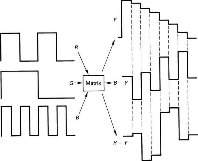
Figure 2.28(a) shows an SMPTE/EBU standard colour difference signal set in which the signals are called Ys, Ph and Pr. 0.3 V syncs are on luma only and all three video signals have a 0.7 V peak-to-peak swing with 100 per cent bars. In order to obtain these voltage swings, the following gain corrections are made to the components:
Figure 2.28 (a) 100 per cent colour bars represented by SMPTE/EBU standard colour difference signals. (b) Level comparison is easier in waveform monitors if the B-Y and R-Y signals are offset upwards.

Within waveform monitors, the colour difference signals may be offset by 350 mV as in Figure 2.28(b) to match the luma range for display purposes.
2.10 Motion portrayal and dynamic resolution
As the eye uses involuntary tracking at all times, the criterion for measuring the definition of moving-image portrayal systems has to be dynamic resolution, defined as the apparent resolution perceived by the viewer in an object moving within the limits of accurate eye tracking. The traditional metric of static resolution in film and television has to be abandoned as unrepresentative.
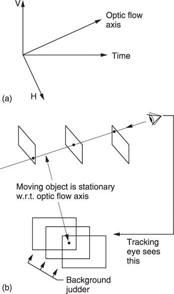
Figure 2.29(a) shows that when the moving eye tracks an object on the screen, the viewer is watching with respect to the optic flow axis, not the time axis, and these are not parallel when there is motion. The optic flow axis is defined as an imaginary axis in the spatio-temporal volume which joins the same points on objects in successive frames. Clearly, when many objects move independently there will be one optic flow axis for each.
Figure 2.29 The optic flow axis (a) joins points on a moving object in successive pictures. (b) When a tracking eye follows a moving object on a screen, that screen will be seen in a different place at each picture. This is the origin of background strobing.
The optic flow axis is identified by motion-compensated standards convertors to eliminate judder and also by MPEG compressors because the greatest similarity from one picture to the next is along that axis. The success of these devices is testimony to the importance of the theory.
Figure 2.29(b) shows that when the eye is tracking, successive pictures appear in different places with respect to the retina. In other words if an object is moving down the screen and followed by the eye, the raster is actually moving up with respect to the retina. Although the tracked object is stationary with respect to the retina and temporal frequencies are zero, the object is moving with respect to the sensor and the display and in those units high temporal frequencies will exist. If the motion of the object on the sensor is not correctly portrayed, dynamic resolution will suffer.
In real-life eye tracking, the motion of the background will be smooth, but in an image-portrayal system based on periodic presentation of frames, the background will be presented to the retina in a different position in each frame. The retina seperately perceives each impression of the background leading to an effect called background strobing.
The criterion for the selection of a display frame rate in an imaging system is sufficient reduction of background strobing. It is a complete myth that the display rate simply needs to exceed the critical flicker frequency. Manufacturers of graphics displays which use frame rates well in excess of those used in film and television are doing so for a valid reason: it gives better results! Note that the display rate and the transmission rate need not be the same in an advanced system.
Dynamic resolution analysis confirms that both interlaced television and conventionally projected cinema film are both seriously sub-optimal. In contrast, progressively scanned television systems have no such defects.
2.11 Progressive or interlaced scan?
Interlaced scanning is a crude compression technique which was developed empirically in the 1930s as a way of increasing the picture rate to reduce flicker without increasing the video bandwidth. Instead of transmitting entire frames, the lines of the frame are sorted into odd lines and even lines. Odd lines are transmitted in one field, even lines in the next. A pair of fields will interlace to produce a frame. Vertical detail such as an edge may only be present in one field of the pair and this results in frame rate flicker called ‘interlace twitter’.
Figure 2.30(a) shows a dynamic resolution analysis of interlaced scanning. When there is no motion, the optic flow axis and the time axis are parallel and the apparent vertical sampling rate is the number of lines in a frame. However, when there is vertical motion, (b), the optic flow axis turns. In the case shown, the sampling structure due to interlace results in the vertical sampling rate falling to one half of its stationary value.
Figure 2.30 When an interlaced picture is stationary, viewing takes place along the time axis as shown in (a). When a vertical component of motion exists, viewing takes place along the optic flow axis, (b) The vertical sampling rate falls to one half its stationary value, (c) The halving in sampling rate causes high spatial frequencies to alias.

Consequently interlace does exactly what would be expected from a half-bandwidth filter. It halves the vertical resolution when any motion with a vertical component occurs. In a practical television system, there is no anti-aliasing filter in the vertical axis and so when the vertical sampling rate of an interlaced system is halved by motion, high spatial freqiencies will alias or heterodyne causing annoying artifacts in the picture. This is easily demonstrated.
Figure 2.30(c) shows how a vertical spatial frequency well within the static resolution of the system aliases when motion occurs. In a progressive scan system this effect is absent and the dynamic resolution due to scanning can be the same as the static case.
This analysis also illustrates why interlaced television systems have to have horizontal raster lines. This is because in real life, horizontal motion is more common than vertical. It is easy to calculate the vertical image motion velocity needed to obtain the half-bandwidth speed of interlace, because it amounts to one raster line per field. In 525/60 (NTSC) there are about 500 active lines, so motion as slow as one picture height in 8 seconds will halve the dynamic resolution. In 625/50 (PAL) there are about 600 lines, so the half-bandwidth speed falls to one picture height in 12 seconds. This is why NTSC, with fewer lines and lower bandwidth, doesn’t look as soft as it should compared to PAL, because it has better dynamic resolution.
The situation deteriorates rapidly if an attempt is made to use interlaced scanning in systems with a lot of lines. In 1250/50, the resolution is halved at a vertical speed of just one picture height in 24 seconds. In other words on real moving video a 1250/50 interlaced system has the same dynamic resolution as a 625/50 progressive system. By the same argument a 1080 I system has the same performance as a 480 P system.
2.12 Binary codes
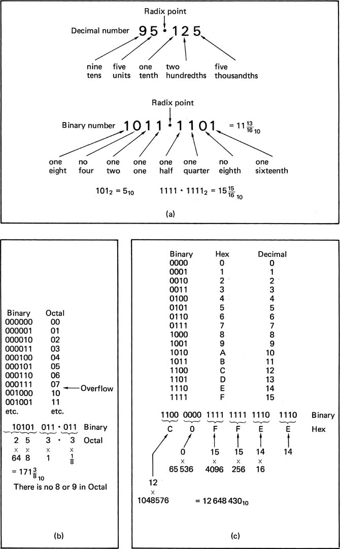
For digital video use, the prime purpose of binary numbers is to express the values of the samples which represent the original analog video waveform. Figure 2.31 shows some binary numbers and their equivalent in decimal. The radix point has the same significance in binary: symbols to the right of it represent one half, one quarter and so on. Binary is convenient for electronic circuits, which do not get tired, but numbers expressed in binary become very long, and writing them is tedious and error-prone. The octal and hexadecimal notations are both used for writing binary since conversion is so simple. Figure 2.31 also shows that a binary number is split into groups of three or four digits starting at the least significant end, and the groups are individually converted to octal or hexadecimal digits. Since sixteen different symbols are required in hex. the letters A – F are used for the numbers above nine.
Figure 2.31 (a) Binary and decimal; (b) In octal, groups of three bits make one symbol 0–7. (c) In hex, groups of four bits make one symbol O-F. Note how much shorter the number is in hex.
There will be a fixed number of bits in a PCM video sample, and this number determines the size of the quantizing range. In the eight-bit samples used in much digital video equipment, there are 256 different numbers. Each number represents a different analog signal voltage, and care must be taken during conversion to ensure that the signal does not go outside the convertor range, or it will be clipped. In Figure 2.32(a) it will be seen that in an eight-bit pure binary system, the number range goes from 00 hex, which represents the smallest voltage, through to FF hex, which represents the largest positive voltage. The video waveform must be accommodated within this voltage range, and (b) shows how this can be done for a PAL composite signal. A luminance signal is shown in (c). As component digital systems only handle the active line, the quantizing range is optimized to suit the gamut of the unblanked luminance. There is a small offset in order to handle slightly maladjusted inputs.
Figure 2.32 The unipolar quantizing range of an eight-bit pure binary system is shown at (a). The analog input must be shifted to fit into the quantizing range, as shown for PAL at (b). In component, sync pulses are not digitized, so the quantizing intervals can be smaller as at (c). An offset of half scale is used for colour difference signals (d).

Colour difference signals are bipolar and so blanking is in the centre of the signal range. In order to accommodate colour difference signals in the quantizing range, the blanking voltage level of the analog waveform has been shifted as in Figure 2.32(d) so that the positive and negative voltages in a real video signal can be expressed by binary numbers which are only positive. This approach is called offset binary. Strictly speaking, both the composite and luminance signals are also offset binary because the blanking level is part-way up the quantizing scale.
Offset binary is perfectly acceptable where the signal has been digitized only for recording or transmission from one place to another, after which it will be converted directly back to analog. Under these conditions it is not necessary for the quantizing steps to be uniform, provided both ADC and DAC are constructed to the same standard. In practice, it is the requirements of signal processing in the digital domain which make both non-uniform quantizing and offset binary unsuitable.
Figure 2.33 shows that analog video signal voltages are referred to blanking. The level of the signal is measured by how far the waveform deviates from blanking, and attenuation, gain and mixing all take place around blanking level. Digital vision mixing is achieved by adding sample values from two or more different sources, but unless all the quantizing intervals are of the same size and there is no offset, the sum of two sample values will not represent the sum of the two original analog voltages. Thus sample values which have been obtained by non-uniform or offset quantizing cannot readily be processed because the binary numbers are not proportional to the signal voltage.
Figure 2.33 All video signal voltages are referred to blanking and must be added with respect to that level.

If two offset binary sample streams are added together in an attempt to perform digital mixing, the result will be that the offsets are also added and this may lead to an overflow. Similarly, if an attempt is made to attenuate by, say, 6.02 dB by dividing all the sample values by two, Figure 2.34 shows that the offset is also divided and the waveform suffers a shifted baseline. This problem can be overcome with digital luminance signals simply by subtracting the offset from each sample before processing as this results in numbers truly proportional to the luminance voltage. This approach is not suitable for colour difference or composite signals because negative numbers would result when the analog voltage goes below blanking and pure binary coding cannot handle them. The problem with offset binary is that it works with reference to one end of the range. What is needed is a numbering system which operates symmetrically with reference to the centre of the range.
Figure 2.34 The result of an attempted attenuation in pure binary code is an offset. Pure binary cannot be used for digital video processing.

In the two’s complement system, the upper half of the pure binary number range has been redefined to represent negative quantities. If a pure binary counter is constantly incremented and allowed to overflow, it will produce all the numbers in the range permitted by the number of available bits, and these are shown for a four-bit example drawn around the circle in Figure 2.35. As a circle has no real beginning, it is possible to consider it to start wherever it is convenient. In two’s complement, the quantizing range represented by the circle of numbers does not start at zero, but starts on the diametrically opposite side of the circle. Zero is midrange, and all numbers with the MSB (most significant bit) set are considered negative. The MSB is thus the equivalent of a sign bit where 1 = minus. Two’s complement notation differs from pure binary in that the most significant bit is inverted in order to achieve the half-circle rotation.
Figure 2.35 In this example of a four-bit two’s complement code, the number range is from -8 to +7. Note that the MSB determines polarity.

Figure 2.36 shows how a real ADC is configured to produce two’s complement output. At (a) an analog offset voltage equal to one half the quantizing range is added to the bipolar analog signal in order to make it unipolar as at (b). The ADC produces positive only numbers at (c) which are proportional to the input voltage. The MSB is then inverted at (d) so that the all-zeros code moves to the centre of the quantizing range. The analog offset is often incorporated into the ADC as is the MSB inversion. Some convertors are designed to be used in either pure binary or two’s complement mode. In this case the designer must arrange the appropriate DC conditions at the input. The MSB inversion may be selectable by an external logic level. In the digital video interface standards the colour difference signals use offset binary because the codes of all zeros and all ones are at the end of the range and can be reserved for synchronizing. A digital vision mixer simply inverts the MSB of each colour difference sample to convert it to two’s complement.
Figure 2.36 A two’s complement ADC. At (a) an analog offset voltage equal to one-half the quantizing range is added to the bipolar analog signal in order to make it unipolar as at (b). The ADC produces positive only numbers at (c), but the MSB is then inverted at (d) to give a two’s complement output.

The two’s complement system allows two sample values to be added, or mixed in video parlance, and the result will be referred to the system midrange; this is analogous to adding analog signals in an operational amplifier.
Figure 2.37 illustrates how adding two’s complement samples simulates a bipolar mixing process. The waveform of input A is depicted by solid black samples, and that of B by samples with a solid outline. The result of mixing is the linear sum of the two waveforms obtained by adding pairs of sample values. The dashed lines depict the output values. Beneath each set of samples is the calculation which will be seen to give the correct result. Note that the calculations are pure binary. No special arithmetic is needed to handle two’s complement numbers.
Figure 2.37 Using two’s complement arithmetic, single values from two waveforms are added together with respect to midrange to give a correct mixing function.

It is sometimes necessary to phase reverse or invert a digital signal. The process of inversion in two’s complement is simple. All bits of the sample value are inverted to form the one’s complement, and one is added. This can be checked by mentally inverting some of the values in Figure 2.35. The inversion is transparent and performing a second inversion gives the original sample values.
Using inversion, signal subtraction can be performed using only adding logic. The inverted input is added to perform a subtraction, just as in the analog domain. This permits a significant saving in hardware complexity, since only carry logic is necessary and no borrow mechanism need be supported.
In summary, two’s complement notation is the most appropriate scheme for bipolar signals, and allows simple mixing in conventional binary adders. It is in virtually universal use in digital video and audio processing.
Two’s complement numbers can have a radix point and bits below it just as pure binary numbers can. It should, however, be noted that in two’s complement, if a radix point exists, numbers to the right of it are added. For example, 1100.1 is not −4.5, it is–4 + 0.5 = 3.5.
2.13 Introduction to digital logic
However complex a digital process, it can be broken down into smaller stages until finally one finds that there are really only two basic types of element in use, and these can be combined in some way and supplied with a clock to implement virtually any process. Figure 2.38 shows that the first type is a logic element. This produces an output which is a logical function of the input with minimal delay. The second type is a storage element which samples the state of the input(s) when clocked and holds or delays that state. The strength of binary logic is that the signal has only two states, and considerable noise and distortion of the binary waveform can be tolerated before the state becomes uncertain. At every logic element, the signal is compared with a threshold, and can thus can pass through any number of stages without being degraded.
Figure 2.38 Logic elements have a finite propagation delay between input and output and cascading them delays the signal an arbitrary amount. Storage elements sample the input on a clock edge and can return a signal to near coincidence with the system clock. This is known as reclocking. Reclocking eliminates variations in propagation delay in logic elements.
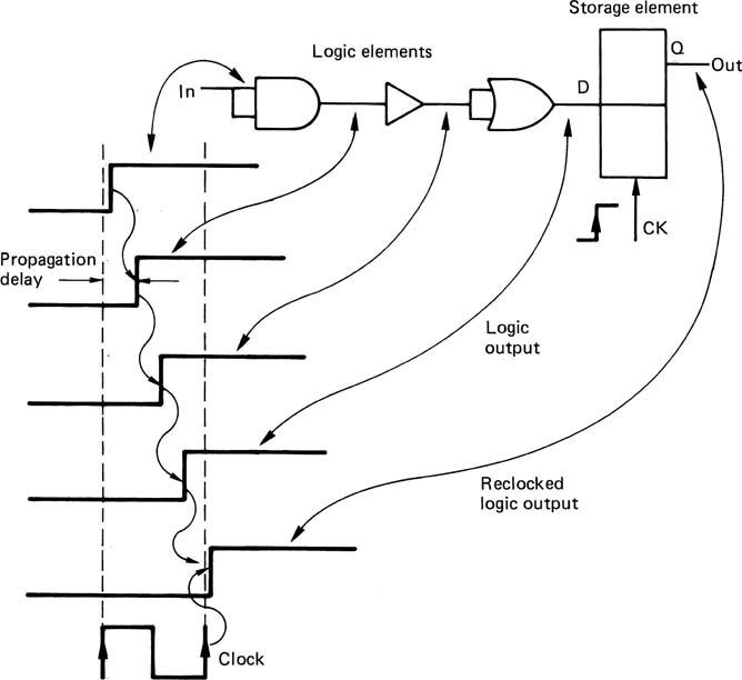
In addition, the use of a storage element at regular locations throughout logic circuits eliminates time variations or jitter. Figure 2.38 shows that if the inputs to a logic element change, the output will not change until the propagation delay of the element has elapsed. However, if the output of the logic element forms the input to a storage element, the output of that element will not change until the input is sampled at the next clock edge. In this way the signal edge is aligned to the system clock and the propagation delay of the logic becomes irrelevant. The process is known as reclocking.
The two states of the signal when measured with an oscilloscope are simply two voltages, usually referred to as high and low. As there are only two states, there can only be true or false meanings. The true state of the signal can be assigned by the designer to either voltage state. When a high voltage represents a true logic condition and a low voltage represents a false condition, the system is known as positive logic, or high true logic. This is the usual system, but sometimes the low voltage represents the true condition and the high voltage represents the false condition. This is known as negative logic or low true logic. Provided that everyone is aware of the logic convention in use, both work equally well.
In logic systems, all logical functions, however complex, can be configured from combinations of a few fundamental logic elements or gates. It is not profitable to spend too much time debating which are the truly fundamental ones, since most can be made from combinations of others. Figure 2.39 shows the important simple gates and their derivatives, and introduces the logical expressions to describe them, which can be compared with the truth-table notation. The figure also shows the important fact that when negative logic is used, the OR gate function interchanges with that of the AND gate.
Figure 2.39 The basic logic gates compared.

If numerical quantities need to be conveyed down the two-state signal paths described here, then the only appropriate numbering system is binary, which has only two symbols, 0 and 1. Just as positive or negative logic could be used for the truth of a logical binary signal, it can also be used for a numerical binary signal. Normally, a high voltage level will represent a binary 1 and a low voltage will represent a binary 0, described as a ‘high for a one’ system. Clearly a ‘low for a one’ system is just as feasible. Decimal numbers have several columns, each of which represents a different power of ten; in binary the column position specifies the power of two.
Several binary digits or bits are needed to express the value of a binary video sample. These bits can be conveyed at the same time by several signals to form a parallel system, which is most convenient inside equipment or for short distances because it is inexpensive, or one at a time down a single signal path, which is more complex, but convenient for cables between pieces of equipment because the connectors require fewer pins. When a binary system is used to convey numbers in this way, it can be called a digital system.
The basic memory element in logic circuits is the latch, which is constructed from two gates as shown in Figure 2.40(a), and which can be set or reset. A more useful variant is the D-type latch shown at (b) which remembers the state of the input at the time a separate clock either changes state for an edge-triggered device, or after it goes false for a level-triggered device. D-type latches are commonly available with four or eight latches to the chip. A shift register can be made from a series of latches by connecting the Q output of one latch to the D input of the next and connecting all the clock inputs in parallel. Data are delayed by the number of stages in the register. Shift registers are also useful for converting between serial and parallel data transmissions.
Figure 2.40 Digital semiconductor memory types. In (a), one data bit can be stored in a simple set-reset latch, which has little application because the D-type latch in (b) can store the state of the single data input when the clock occurs. These devices can be implemented with bipolar transistors or FETs, and are called static memories because they can store indefinitely. They consume a lot of power.
Figure 2.40 In (c), a bit is stored as the charge in a potential well in the substrate of a chip. It is accessed by connecting the bit line with the field effect from the word line. The single well where the two lines cross can then be written or read. These devices are called dynamic RAMs because the charge decays, and they must be read and rewritten (refreshed) periodically.
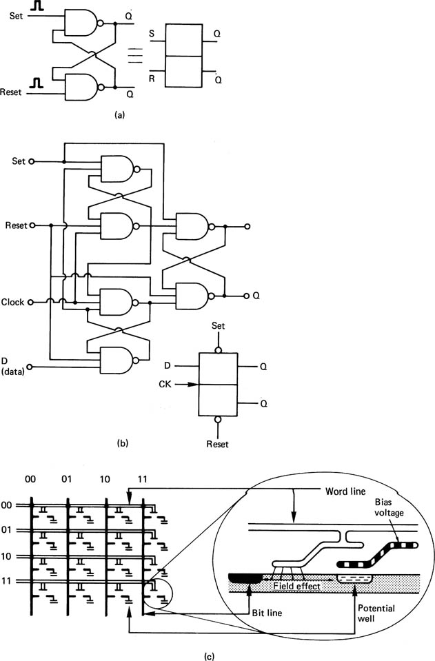
Where large numbers of bits are to be stored, cross-coupled latches are less suitable because they are more complicated to fabricate inside integrated circuits than dynamic memory, and consume more current.
In large random access memories (RAMs), the data bits are stored as the presence or absence of charge in a tiny capacitor as shown in Figure 2.40(c). The capacitor is formed by a metal electrode, insulated by a layer of silicon dioxide from a semiconductor substrate, hence the term MOS (metal oxide semiconductor). The charge will suffer leakage, and the value would become indeterminate after a few milliseconds. Where the delay needed is less than this, decay is of no consequence, as data will be read out before they have had a chance to decay. Where longer delays are necessary, such memories must be refreshed periodically by reading the bit value and writing it back to the same place. Most modern MOS RAM chips have suitable circuitry built-in. Large RAMs store thousands of bits, and it is clearly impractical to have a connection to each one. Instead, the desired bit has to be addressed before it can be read or written. The size of the chip package restricts the number of pins available, so that large memories use the same address pins more than once. The bits are arranged internally as rows and columns, and the row address and the column address are specified sequentially on the same pins.
The circuitry necessary for adding pure binary or two’s complement numbers is shown in Figure 2.41. Addition in binary requires two bits to be taken at a time from the same position in each word, starting at the least significant bit. Should both be ones, the output is zero, and there is a carry-out generated. Such a circuit is called a half adder, shown in Figure 2.41(a) and is suitable for the least significant bit of the calculation. All higher stages will require a circuit which can accept a carry input as well as two data inputs. This is known as a full adder (Figure 2.41(b)). Multibit full adders are available in chip form, and have carryin and carry-out terminals to allow them to be cascaded to operate on long wordlengths. Such a device is also convenient for inverting a two’s complement number, in conjunction with a set of invertors. The adder chip has one set of inputs grounded, and the carry-in permanently held true, such that it adds one to the one’s complement number from the invertor.
Figure 2.41 (a) Half adder; (b) full-adder circuit and truth table; (c) comparison of sign bits prevents wraparound on adder overflow by substituting clipping level.

When mixing by adding sample values, care has to be taken to ensure that if the sum of the two sample values exceeds the number range the result will be clipping rather than wraparound. In two’s complement, the action necessary depends on the polarities of the two signals. Clearly, if one positive and one negative number are added, the result cannot exceed the number range. If two positive numbers are added, the symptom of positive overflow is that the most significant bit sets, causing an erroneous negative result, whereas a negative overflow results in the most significant bit clearing. The overflow control circuit will be designed to detect these two conditions, and override the adder output. If the MSB of both inputs is zero, the numbers are both positive, thus if the sum has the MSB set, the output is replaced with the maximum positive code (0111 …). If the MSB of both inputs is set, the numbers are both negative, and if the sum has no MSB set, the output is replaced with the maximum negative code (1000 …). These conditions can also be connected to warning indicators. Figure 2.41(c) shows this system in hardware. The resultant clipping on overload is sudden, and sometimes a PROM is included which translates values around and beyond maximum to soft-clipped values below or equal to maximum.
A storage element can be combined with an adder to obtain a number of useful functional blocks which will crop up frequently in audio equipment. Figure 2.42(a) shows that a latch is connected in a feedback loop around an adder. The latch contents are added to the input each time it is clocked. The configuration is known as an accumulator in computation because it adds up or accumulates values fed into it. In filtering, it is known as an discrete time integrator. If the input is held at some constant value, the output increases by that amount on each clock. The output is thus a sampled ramp.
Figure 2.42 Two configurations which are common in processing. In (a) the feedback around the adder adds the previous sum to each input to perform accumulation or digital integration. In (b) an inverter allows the difference between successive inputs to be computed. This is differentiation.

Figure 2.42(b) shows that the addition of an invertor allows the difference between successive inputs to be obtained. This is digital differentiation. The output is proportional to the slope of the input.
2.14 The computer
The computer is now a vital part of digital video systems, being used both for control purposes and to process video signals as data. In control, the computer finds applications in database management, automation, editing, and in electromechanical systems such as tape drives and robotic cassette handling. Now that processing speeds have advanced sufficiently, computers are able to manipulate certain types of digital video in real time. Where very complex calculations are needed, real-time operation may not be possible and instead the computation proceeds as fast as it can in a process called rendering. The rendered data are stored so that they can be viewed in real time from a storage medium when the rendering is complete.
The computer is a programmable device in that its operation is not determined by its construction alone, but instead by a series of instructions forming a program. The program is supplied to the computer one instruction at a time so that the desired sequence of events takes place.
Programming of this kind has been used for over a century in electromechanical devices, including automated knitting machines and street organs which are programmed by punched cards. However, the computer differs from these devices in that the program is not fixed, but can be modified by the computer itself. This possibility led to the creation of the term software to suggest a contrast to the constancy of hardware.
Computer instructions are binary numbers each of which is interpreted in a specific way. As these instructions don’t differ from any other kind of data, they can be stored in RAM. The computer can change its own instructions by accessing the RAM. Most types of RAM are volatile, in that they lose data when power is removed. Clearly if a program is entirely stored in this way, the computer will not be able to recover fom a power failure. The solution is that a very simple starting or bootstrap program is stored in non-volatile ROM which will contain instructions that will bring in the main program from a storage system such as a disk drive after power is applied. As programs in ROM cannot be altered, they are sometimes referred to as firmware to indicate that they are classified between hardware and software.
Making a computer do useful work requires more than simply a program which performs the required computation. There is also a lot of mundane activity which does not differ significantly from one program to the next. This includes deciding which part of the RAM will be occupied by the program and which by the data, producing commands to the storage disk drive to read the input data from a file and write back the results. It would be very inefficient if all programs had to handle these processes themselves. Consequently the concept of an operating system was developed. This manages all the mundane decisions and creates an environment in which useful programs or applications can execute.
The ability of the computer to change its own instructions makes it very powerful, but it also makes it vulnerable to abuse. Programs exist which are deliberately written to do damage. These viruses are generally attached to plausible messages or data files and enter computers through storage media or communications paths.
There is also the possibility that programs contain logical errors such that in certain combinations of circumstances the wrong result is obtained. If this results in the unwitting modification of an instruction, the next time that instruction is accessed the computer will crash. In consumer-grade software, written for the vast personal computer market, this kind of thing is unfortunately accepted.
For critical applications, software must be verified. This is a process which can prove that a program can recover from absolutely every combination of circumstances and keep running properly. This is a non-trivial process, because the number of combinations of states a computer can get into is staggering. As a result most software is unverified.
It is of the utmost importance that networked computers which can suffer virus infection or computers running unverified software are never used in a life-support or critical application.
Figure 2.43 shows a simple computer system. The various parts are linked by a bus which allows binary numbers to be transferred from one place to another. This will generally use tri-state logic so that when one device is sending to another, all other devices present a high impedance to the bus.
Figure 2.43 A simple computer system. All components are linked by a single data/address/control bus. Although cheap and flexible, such a bus can only make one connection at a time, so it is slow.

The ROM stores the startup program, the RAM stores the operating system, applications programs and the data to be processed. The disk drive stores large quantities of data in a non-volatile form. The RAM only needs to be able to hold part of one program as other parts can be brought from the disk as required. A program executes by fetching one instruction at a time from the RAM to the processor along the bus.
The bus also allows keyboard/mouse inputs and outputs to the display and printer. Inputs and outputs are generally abbreviated to I/O. Finally a programmable timer will be present which acts as a kind of alarm clock for the processor.
2.15 The processor
The processor or CPU (central processing unit) is the heart of the system. Figure 2.44 shows a simple example of a CPU. The CPU has a bus interface which allows it to generate bus addresses and input or output data. Sequential instructions are stored in RAM at contiguously increasing locations so that a program can be executed by fetching instructions from a RAM address specified by the program counter (PC) to the instruction register in the CPU. As each instruction is completed, the PC is incremented so that it points to the next instruction. In this way the time taken to execute the instruction can vary.
Figure 2.44 The data path of a simple CPU. Under control of an instruction, the ALU will perform some function on a pair of input values from the registers and store or output the result.

The processor is notionally divided into data paths and control paths. Figure 2.44 shows the data path. The CPU contains a number of general-purpose registers or scratchpads which can be used to store partial results in complex calculations. Pairs of these registers can be addressed so that their contents go to the ALU (arithmetic logic unit). This performs various arithmetic (add, subtract, etc.) or logical (and, or, etc.) functions on the input data. The output of the ALU may be routed back to a register or output. By reversing this process it is possible to get data into the registers from the RAM. The ALU also outputs the conditions resulting from the calculation, which can control conditional instructions.
Which function the ALU performs and which registers are involved are determined by the instruction currently in the instruction register then is decoded in the control path. One pass through the ALU can be completed in one cycle of the processor’s clock. Instructions vary in complexity as do the number of clock cycles needed to complete them. Incoming instructions are decoded and used to access a look-up table which converts them into microinstructions, one of which controls the CPU at each clock cycle.
2.16 Timebase correction
In Chapter 1 it was stated that a strength of digital technology is the ease with which delay can be provided. Accurate control of delay is the essence of timebase correction, necessary whenever the instantaneous time of arrival or rate from a data source does not match the destination. In digital video, the destination will almost always have perfectly regular timing, namely the sampling rate clock of the final DAC. Timebase correction consists of aligning jittery signals from storage media or transmission channels with that stable reference.
A further function of timebase correction is to reverse the time compression applied prior to recording or transmission. As was shown in section 1.7, digital recorders compress data into blocks to facilitate editing and error correction as well as to permit head switching between blocks in rotary-head machines. Owing to the spaces between blocks, data arrive in bursts on replay, but must be fed to the output convertors in an unbroken stream at the sampling rate.
In computer hard-disk drives, which are used in digital video workstations, time compression is also used, but a converse problem also arises. Data from the disk blocks arrive at a reasonably constant rate, but cannot necessarily be accepted at a steady rate by the logic because of contention for the use of buses and memory by the different parts of the system. In this case the data must be buffered by a relative of the timebase corrector which is usually referred to as a silo.
Although delay is easily implemented, it is not possible to advance a data stream. Most real machines cause instabilities balanced about the correct timing: the output jitters between too early and too late. Since the information cannot be advanced in the corrector, only delayed, the solution is to run the machine in advance of real time. In this case, correctly timed output signals will need a nominal delay to align them with reference timing. Early output signals will receive more delay, and late output signals will receive less delay.
Section 2.13 showed the principles of digital storage elements which can be used for delay purposes. The shift-register approach and the RAM approach to delay are very similar, as a shift register can be thought of as a memory whose address increases automatically when clocked. The data rate and the maximum delay determine the capacity of the RAM required. Figure 2.45 shows that the addressing of the RAM is by a counter that overflows endlessly from the end of the memory back to the beginning, giving the memory a ring-like structure. The write address is determined by the incoming data, and the read address is determined by the outgoing data. This means that the RAM has to be able to read and write at the same time. The switching between read and write involves not only a data multiplexer but also an address multiplexer. In general the arbitration between read and write will be done by signals from the stable side of the TBC as Figure 2.46 shows. In the replay case the stable clock will be on the read side. The stable side of the RAM will read a sample when it demands, and the writing will be locked out for that period. The input data cannot be interrupted in many applications, however, so a small buffer silo is installed before the memory, which fills up as the writing is locked out, and empties again as writing is permitted. Alternatively, the memory will be split into blocks as was shown in Chapter 1, such that when one block is reading a different block will be writing and the problem does not arise.
Figure 2.45 Most TBCs are implemented as a memory addressed by a counter which periodically overflows to give a ring structure. The memory allows the read and write sides to be asynchronous.

Figure 2.46 In a RAM-based TBC, the RAM is reference synchronous, and an arbitrator decides when it will read and when it will write. During reading, asynchronous input data back up in the input silo, asserting a write request to the arbitrator. Arbitrator will then cause a write cycle between read cycles.
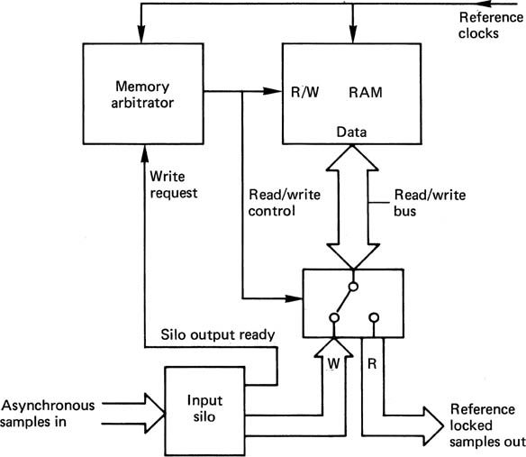
In most digital video applications, the sampling rate exceeds the rate at which economically available RAM chips can operate. The solution is to arrange several video samples into one longer word, known as a superword, and to construct the memory so that it stores superwords in parallel.
Figure 2.47 shows the operation of a FIFO chip, colloquially known as a silo because the data are tipped in at the top on delivery and drawn off at the bottom when needed. Each stage of the chip has a data register and a small amount of logic, including a data-valid or V bit. If the input register does not contain data, the first V bit will be reset, and this will cause the chip to assert ‘input ready’. If data are presented at the input, and clocked into the first stage, the V bit will set, and the ‘input ready’ signal will become false. However, the logic associated with the next stage sees the V bit set in the top stage, and if its own V bit is clear, it will clock the data into its own register, set its own V bit, and clear the input V bit, causing ‘input ready’ to reassert, when another word can be fed in. This process then continues as the word moves down the silo, until it arrives at the last register in the chip. The V bit of the last stage becomes the ‘output ready’ signal, telling subsequent circuitry that there are data to be read. If this word is not read, the next word entered will ripple down to the stage above. Words thus stack up at the bottom of the silo. When a word is read out, an external signal must be provided which resets the bottom V bit. The ‘output ready’ signal now goes false, and the logic associated with the last stage now sees valid data above, and loads down the word when it will become ready again. The last register but one will now have no V bit set, and will see data above itself and bring that down. In this way a reset V bit propagates up the chip while the data ripple down, rather like a hole in a semiconductor going the opposite way to the electrons. Silo chips are usually available in four-bit wordlengths, but can easily be connected in parallel to form superwords. Silo chips are asynchronous, and paralleled chips will not necessarily all work at the same speed. This problem is easily overcome by ‘anding’ together all of the input-ready and output-ready signals and parallel-connecting the strobes. Figure 2.48 shows this mode of operation.
Figure 2.47 Structure of FIFO or silo chip. Ripple logic controls propagation of data down silo.

Figure 2.48 In this example, a twenty-bit wordlength silo is made from five parallel FIFO chips. The asynchronous ripple action of FIFOs means that it is necessary to ‘AND’ together the ready signals.

When used in a hard-disk system, a silo will allow data to and from the disk, which is turning at constant speed. When reading the disk, Figure 2.49(a) shows that the silo starts empty, and if there is bus contention, the silo will start to fill. Where the bus is free, the disk controller will attempt to empty the silo into the memory. The system can take advantage of the interblock gaps on the disk, containing headers, preambles and redundancy, for in these areas there are no data to transfer, and there is some breathing space to empty the silo before the next block. In practice the silo need not be empty at the start of every block, provided it never becomes full before the end of the transfer. If this happens some data are lost and the function must be aborted. The block containing the silo overflow will generally be reread on the next revolution. In sophisticated systems, the silo has a kind of dipstick, and can interrupt the CPU if the data get too deep. The CPU can then suspend some bus activity to allow the disk controller more time to empty the silo.
Figure 2.49 The silo contents during read functions (a) appear different from those during write functions (b). In (a), the control logic attempts to keep the silo as empty as possible; in (b) the logic prefills the silo and attempts to keep it full until the memory word count overflows.

When the disk is to be written, as in Figure 2.49(b), a continuous data stream must be provided during each block, as the disk cannot stop. The silo will be prefilled before the disk attempts to write, and the disk controller attempts to keep it full. In this case all will be well if the silo does not become empty before the end of the transfer. Figure 2.50 shows the silo of a typical disk controller with the multiplexers necessary to put it in the read data stream or the write data stream.
Figure 2.50 In order to guarantee that the drive can transfer data in real time at regular intervals (determined by disk speed and density) the silo provides buffering to the asynchronous operation of the memory access process. At (a) the silo is configured for a disk read. The same silo is used at (b) for a disk write.

2.17 Multiplexing
Multiplexing is used where several signals are to be transmitted down the same channel. The channel bit rate must be the same as or greater than the sum of the source bit rates. Figure 2.51 shows that when multiplexing is used, the data from each source have to be time compressed. This is done by buffering source data in a memory at the multiplexer. It is written into the memory in real time as it arrives, but will be read from the memory with a clock which has a much higher rate. This means that the readout occurs in a smaller timespan. If, for example, the clock frequency is raised by a factor of ten, the data for a given signal will be transmitted in a tenth of the normal time, leaving time in the multiplex for nine more such signals.
Figure 2.51 Multiplexing requires time compression on each input.
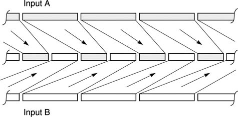
In the demultiplexer another buffer memory will be required. Only the data for the selected signal will be written into this memory at the bit rate of the multiplex. When the memory is read at the correct speed, the data will emerge with their original timebase.
In practice it is essential to have mechanisms to identify the separate signals to prevent them being mixed up and to convey the original signal clock frequency to the demultiplexer. In time-division multiplexing the timebase of the transmission is broken into equal slots, one for each signal. This makes it easy for the demultiplexer, but forces a rigid structure on all the signals such that they must all be locked to one another and have an unchanging bit rate. Packet multiplexing overcomes these limitations.
The multiplexer must switch between different time-compressed signals to create the bitstream and this is much easier to organize if each signal is in the form of data packets of constant size. Figure 2.52 shows a packet multiplexing system.
Each packet consists of two components: the header, which identifies the packet, and the payload, which is the data to be transmitted. The header will contain at least an identification code (ID) which is unique for each signal in the multiplex. The demultiplexer checks the ID codes of all incoming packets and discards those which do not have the wanted ID.
Figure 2.52 Packet multiplexing relies on headers to identify the packets.

In complex systems it is common to have a mechanism to check that packets are not lost or repeated. This is the purpose of the packet continuity count which is carried in the header. For packets carrying the same ID, the count should increase by one from one packet to the next. Upon reaching the maximum binary value, the count overflows and recommences.
2.18 Statistical multiplexing
Packet multiplexing has advantages over time-division multiplexing because it does not set the bit rate of each signal. A demultiplexer simply checks packet IDs and selects all packets with the wanted code. It will do this however frequently such packets arrive. Consequently it is practicable to have variable bit rate signals in a packet multiplex. The multiplexer has to ensure that the total bit rate does not exceed the rate of the channel, but that rate can be allocated arbitrarily between the various signals.
As a practical matter is is usually necessary to keep the bit rate of the multiplex constant. With variable rate inputs this is done by creating null packets which are generally called stuffing or packing. The headers of these packets contain an unique ID which the demultiplexer does not recognize and so these packets are discarded on arrival.
In an MPEG environment, statistical multiplexing can be extremely useful because it allows for the varying difficulty of real program material. In a multiplex of several television programs, it is unlikely that all the programs will encounter difficult material simultaneously. When one program encounters a detailed scene or frequent cuts which are hard to compress, more data rate can be allocated at the allowable expense of the remaining programs which are handling easy material.
2.19 Filters and transforms
One of the most important processes in digital video is filtering, and its parallel topic of transforms. Filters and transforms are relevant to sampling, displays, recording, transmission and compression systems.
Figure 2.53 shows an optical system of finite resolution. If an object containing an infinitely sharp line is presented to this system, the image will be a symmetrical intensity function known in optics as a point spread function which is a spatial impulse response. All images passing through the optical system are convolved with it.
Figure 2.53 In optical systems an infinitely sharp line is reproduced as a point spread function (a) which is the impulse response of the optical path. Scanning either object or image produces an analog time-variant waveform (b). The scanned object waveform can be converted to the scanned image waveform with an electrical filter having an impulse response which is an analog of the point spread function. (c) The object and image may also be sampled or the object samples can be converted to the image samples by a filter with an analogous discrete impulse response.

Figure 2.53(b) shows that the object may be scanned by an analog system to produce a waveform. The image may also be scanned in this way. These waveforms are now temporal. However, the second waveform may be obtained in another way, using an analog filter in series with the first scanned waveform which has an equivalent impulse response. This filter must have linear phase, i.e. its impulse response must be symmetrical in order to replicate the point spread function.
Figure 2.53(c) shows that the object may also be sampled in which case all samples but one will have a value of zero. The image may also be sampled, and owing to the point spread function, there will now be a number of non-zero sample values. However, the image samples may also be obtained by passing the input sample into a digital filter having the appropriate impulse response. Note that it is possible to obtain the same result as (c) by passing the scanned waveform of (b) into an ADC and storing the samples in a memory.
It should be clear from Figure 2.53 why video signal paths need to have linear phase. In general, analog circuitry and filters tend not to have linear phase because they must be causal which means that the output can only occur after the input. Figure 2.54(a) shows a simple RC network and its impulse response. This is the familiar exponential decay due to the capacitor discharging through the resistor (in series with the source impedance which is assumed here to be negligible). The figure also shows the response to a squarewave at (b). With other waveforms the process is inevitably more complex.
Figure 2.54 (a) The impulse response of a simple RC network is an exponential decay. This can used to calculate the response to a square wave, as in (b).

Filtering is unavoidable. Sometimes a process has a filtering effect which is undesirable, for example the limited frequency response of a CRT drive amplifier or loss of resolution in a lens, and we try to minimize it. On other occasions a filtering effect is specifically required. Analog or digital filters, and sometimes both, are required in ADCs, DACs, in the data channels of digital recorders and transmission systems and in DSP. Optical filters may also be necessary in imaging systems to convert between sampled and continuous images. Optical systems used in displays and in laser recorders also act as spatial filters.1
Figure 2.55 shows that impulse response testing tells a great deal about a filter. In a perfect filter, all frequencies should experience the same time delay. If some groups of frequencies experience a different delay from others, there is a group-delay error. As an impulse contains an infinite spectrum, a filter suffering from group-delay error will separate the different frequencies of an impulse along the time axis.
Figure 2.55 Group delay time-displaces signals as a function of frequency.

A pure delay will cause a phase shift proportional to frequency, and a filter with this characteristic is said to be phase-linear. The impulse response of a phase-linear filter is symmetrical. If a filter suffers from group-delay error it cannot be phase-linear. It is almost impossible to make a perfectly phase-linear analog filter, and many filters have a group-delay equalization stage following them which is often as complex as the filter itself. In the digital domain it is straightforward to make a phase-linear filter, and phase equalization becomes unnecessary.
Because of the sampled nature of the signal, whatever the response at low frequencies may be, all PCM channels act as low-pass filters because they cannot contain frequencies above the Nyquist limit of half the sampling frequency.
Transforms are a useful subject because they can help to understand processes which cause undesirable filtering or to design filters. The information itself may be subject to a transform. Transforming converts the information into another analog. The information is still there, but expressed with respect to temporal or spatial frequency rather than time or space. Instead of binary numbers representing the magnitude of samples, there are binary numbers representing the magnitude of frequency coefficients. What happens in the frequency domain must always be consistent with what happens in the time or space domains. Every combination of frequency and phase response has a corresponding impulse response in the time domain.
Figure 2.56 shows the relationship between the domains. On the left is the frequency domain. Here an input signal having a given spectrum is input to a filter having a given frequency response. The output spectrum will be the product of the two functions. If the functions are expressed logarithmically in deciBels, the product can be obtained by simple addition.
Figure 2.56 If a signal having a given spectrum is passed into a filter, multiplying the two spectra will give the output spectrum at (a). Equally transforming the filter frequency response will yield the impulse response of the filter. If this is convolved with the time domain waveform, the result will be the output waveform, whose transform is the output spectrum (b).

On the right, the time-domain output waveform represents the convolution of the impulse response with the input waveform. However, if the frequency transform of the output waveform is taken, it must be the same as the result obtained from the frequency response and the input spectrum. This is a useful result because it means that when image or audio sampling is considered, it will be possible to explain the process in both domains.
When a waveform is input to a system, the output waveform will be the convolution of the input waveform and the impulse response of the system. Convolution can be followed by reference to a graphic example in Figure 2.57. Where the impulse response is asymmetrical, the decaying tail occurs after the input. As a result it is necessary to reverse the impulse response in time so that it is mirrored prior to sweeping it through the input waveform. The output voltage is proportional to the shaded area shown where the two impulses overlap. If the impulse response is symmetrical, as would be the case with a linear phase filter, or in an optical system, the mirroring process is superfluous.
Figure 2.57 In the convolution of two continuous signals (the impulse response with the input), the impulse must be time reversed or mirrored. This is necessary because the impulse will be moved from left to right, and mirroring gives the impulse the correct time-domain response when it is moved past a fixed point. As the impulse response slides continuously through the input waveform, the area where the two overlap determines the instantaneous output amplitude. This is shown for five different times by the crosses on the output waveform.

The same process can be performed in the sampled, or discrete time domain as shown in Figure 2.58. The impulse and the input are now a set of discrete samples which clearly must have the same sample spacing. The impulse response only has value where impulses coincide. Elsewhere it is zero. The impulse response is therefore stepped through the input one sample period at a time. At each step, the area is still proportional to the output, but as the time steps are of uniform width, the area is proportional to the impulse height and so the output is obtained by adding up the lengths of overlap. In mathematical terms, the output samples represent the convolution of the input and the impulse response by summing the coincident cross-products.
Figure 2.58 In discrete time convolution, the mirrored impulse response is stepped through the input one sample period at a time. At each step, the sum of the cross-products is used to form an output value. As the input in this example is a constant height pulse, the output is simply proportional to the sum of the coincident impulse response samples. This figure should be compared with Figure 2.57.
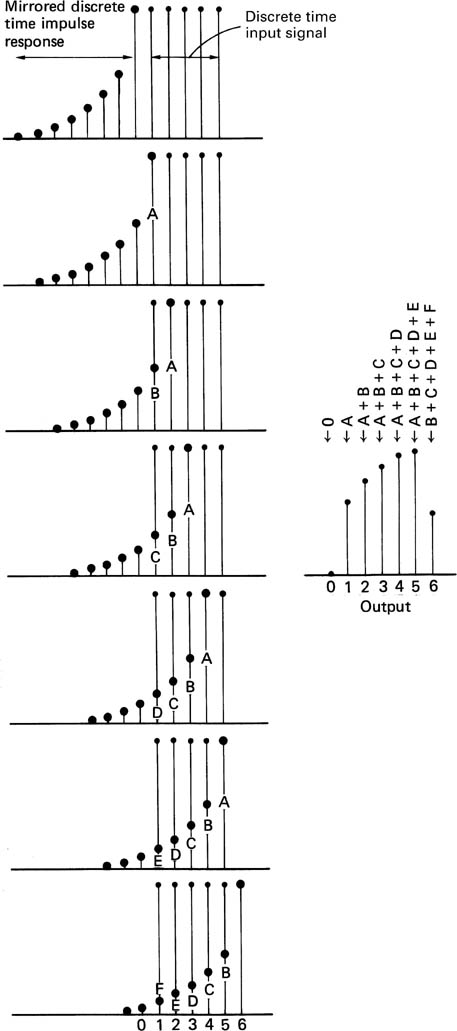
Filters can be described in two main classes, as shown in Figure 2.59, according to the nature of the impulse response. Finite-impulse response (FIR) filters are always stable and, as their name suggests, respond to an impulse once, as they have only a forward path. In the temporal domain, the time for which the filter responds to an input is finite, fixed and readily established. The same is therefore true about the distance over which a FIR filter responds in the spatial domain. FIR filters can be made perfectly phase-linear if a significant processing delay is accepted. Most filters used for image processing, sampling rate conversion and oversampling fall into this category.
Figure 2.59 An FIR filter (a) responds only once to an input, whereas the output of an IIR filter (b) continues indefinitely rather like a decaying echo.

Infinite-impulse response (IIR) filters respond to an impulse indefinitely and are not necessarily stable, as they have a return path from the output to the input. For this reason they are also called recursive filters. As the impulse response is not symmetrical, IIR filters are not phase-linear. Audio equalizers often employ recursive filters.
2.20 FIR filters
A FIR filter performs convolution of the input waveform with its own impulse response. It does this by graphically constructing the impulse response for every input sample and superimposing all these responses. It is first necessary to establish the correct impulse response. Figure 2.60(a) shows an example of a low-pass filter which cuts off at ¼ of the sampling rate. The impulse response of an ideal low-pass filter is a sinx/x curve, where the time between the two central zero crossings is the reciprocal of the cut-off frequency. According to the mathematics, the waveform has always existed, and carries on for ever.
Figure 2.60a The impulse response of an LPF is a sinx/x curve which stretches from -χ to in time. The ends of the response must be neglected, and a delay introduced to make the filter causal.

The peak value of the output coincides with the input impulse. This means that the filter cannot be causal, because the output has changed before the input is known. Thus in all practical applications it is necessary to truncate the extreme ends of the impulse response, which causes an aperture effect, and to introduce a time delay in the filter equal to half the duration of the truncated impulse in order to make the filter causal. As an input impulse is shifted through the series of registers in Figure 2.60(b), the impulse response is created, because at each point it is multiplied by a coefficient as in Figure 2.60(c).
Figure 2.60b The structure of an FIR LPF. Input samples shift across the register and at each point are multiplied by different coefficients.

Figure 2.60c When a single unit sample shifts across the circuit of Figure 2.60(b), the impulse response is created at the output as the impulse is multiplied by each coefficient in turn.

These coefficients are simply the result of sampling and quantizing the desired impulse response. Clearly the sampling rate used to sample the impulse must be the same as the sampling rate for which the filter is being designed. In practice the coefficients are calculated, rather than attempting to sample an actual impulse response. The coefficient wordlength will be a compromise between cost and performance. Because the input sample shifts across the system registers to create the shape of the impulse response, the configuration is also known as a transversal filter. In operation with real sample streams, there will be several consecutive sample values in the filter registers at any time in order to convolve the input with the impulse response.
Simply truncating the impulse response causes an abrupt transition from input samples which matter and those which do not. Truncating the filter superimposes a rectangular shape on the time-domain impulse response. In the frequency domain the rectangular shape transforms to a sinx/x characteristic which is superimposed on the desired frequency response as a ripple. One consequence of this is known as Gibb’s phenomenon; a tendency for the response to peak just before the cut-off frequency.2, 3 As a result, the length of the impulse which must be considered will depend not only on the frequency response, but also on the amount of ripple which can be tolerated. If the relevant period of the impulse is measured in sample periods, the result will be the number of points or multiplications needed in the filter. Figure 2.61 compares the performance of filters with different numbers of points. A high-quality digital audio FIR filter may need in excess of 100 points.
Figure 2.61 The truncation of the impulse in an FIR filter caused by the use of a finite number of points (N) results in ripple in the response. Shown here are three different numbers of points for the same impulse response. The filter is an LPF which rolls off at 0.4 of the fundamental interval. (Courtesy Philips Technical Review.)
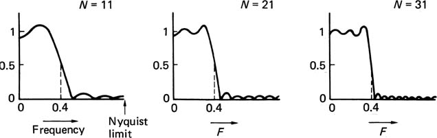
Rather than simply truncate the impulse response in time, it is better to make a smooth transition from samples which do not count to those that do. This can be done by multiplying the coefficients in the filter by a window function which peaks in the centre of the impulse. In the example of Figure 2.62, a low-pass FIR filter is shown which is intended to allow downsampling by a factor of two. The key feature is that the stopband must have begun before one half of the output sampling rate. This is most readily achieved using a Hamming window because it was designed empirically to have a flat stopband so that good aliasing attenuation is possible. The width of the transition band determines the number of significant sample periods embraced by the impulse. The Hamming window doubles the width of the transition band. This determines in turn both the number of points in the filter and the filter delay. For the purposes of illustration, the number of points is much smaller than would normally be the case.
Figure 2.62 A downsampling filter using the Hamming window.

As the impulse is symmetrical, the delay will be half the impulse period. The impulse response is a sinx/x function, and this has been calculated in the figure. The equation for the Hamming window function is shown with the window values which result. The sinx/x response is next multiplied by the Hamming window function to give the windowed impulse response shown.
If the coefficients are not quantized finely enough, it will be as if they had been calculated inaccurately, and the performance of the filter will be less than expected. Figure 2.63 shows an example of quantizing coefficients. Conversely, raising the wordlength of the coefficients increases cost.
Figure 2.63 Frequency response of a 49-point transversal filter with infinite precision (solid line) shows ripple due to finite window size. Quantizing coefficients to twelve bits reduces attenuation in the stopband. (Responses courtesy Philips Technical Review.)
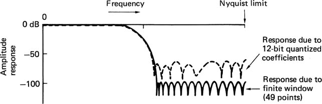
The FIR structure is inherently phase-linear because it is easy to make the impulse response absolutely symmetrical. The individual samples in a digital system do not know in isolation what frequency they represent, and they can only pass through the filter at a rate determined by the clock. Because of this inherent phase-linearity, a FIR filter can be designed for a specific impulse response, and the frequency response will follow.
The frequency response of the filter can be changed at will by changing the coefficients. A programmable filter only requires a series of PROMs to supply the coefficients; the address supplied to the PROMs will select the response. The frequency response of a digital filter will also change if the clock rate is changed, so it is often less ambiguous to specify a frequency of interest in a digital filter in terms of a fraction of the fundamental interval rather than in absolute terms. The configuration shown in Figure 2.60 serves to illustrate the principle. The units used on the diagrams are sample periods and the response is proportional to these periods or spacings, and so it is not necessary to use actual figures.
Where the impulse response is symmetrical, it is often possible to reduce the number of multiplications, because the same product can be used twice, at equal distances before and after the centre of the window. This is known as folding the filter. A folded filter is shown in Figure 2.64.
Figure 2.64 A seven-point folded filter for a symmetrical impulse response. In this case K1 and K7 will be identical, and so the input sample can be multiplied once, and the product fed into the output shift system in two different places. The centre coefficient K4 appears once. In an even-numbered filter the centre coefficient would also be used twice.
2.21 Sampling-rate conversion
Sampling-rate conversion or interpolation is an important enabling technology on which a large number of practical digital video devices are based. In digital video, the sampling rate takes on many guises. When analog video is sampled in real time, the sampling rate is temporal, but where pixels form a static array, the sampling rate is a spatial frequency.
Some of the applications of interpolation are set out here:
1 Video standards convertors need to change two of the sampling rates of the signal they handle, namely the temporal frame rate and the vertical line spacing, which is in fact a spatial sampling frequency. In some low-bit rate video applications such as Internet video, the frame rate may deliberately be reduced. The display will have to increase it again to avoid flicker.
2 To take advantage of oversampling convertors, an increase in sampling rate is necessary for DACs and a reduction in sampling rate is necessary for ADCs. In oversampling the factors by which the rates are changed are simpler than in other applications.
3 In image processing, a large number of different standard pixel array sizes exists. Changing between these formats may be necessary in order to view an incoming image on an avilable display. This technique is generally known as resizing and is essentially a two-dimensional sampling rate conversion. The rate in this case is the spatial frequency of the pixels.
There are three basic but related categories of rate conversion, as shown in Figure 2.65. The most straightforward (a) changes the rate by an integer ratio, up or down. The timing of the system is thus simplified because all samples (input and output) are present on edges of the higher-rate sampling clock. Such a system is generally adopted for oversampling convertors; the exact sampling rate immediately adjacent to the analog domain is not critical, and will be chosen to make the filters easier to implement.
Figure 2.65 Categories of rate conversion. (a) Integer-ratio conversion, where the lower-rate samples are always coincident with those of the higher rate. There are a small number of phases needed. (b) Fractional-ratio conversion, where sample coincidence is periodic. A larger number of phases is required. Example here is conversion from 50.4 kHz to 44.1kHz (8/7). (c) Variable-ratio conversion, where there is no fixed relationship, and a large number of phases are required.
Next in order of difficulty is the category shown at (b) where the rate is changed by the ratio of two small integers. Samples in the input periodically time-align with the output. Such devices can be used for converting between the various rates of ITU–601.
The most complex rate-conversion category is where there is no simple relationship between input and output sampling rates, and in fact they may vary. This situation, shown at (c), is known as variable-ratio conversion. The temporal or spatial relationship of input and output samples is arbitrary. This problem will be met in effects machines which zoom or rotate images.
The technique of integer-ratio conversion is used in conjunction with oversampling convertors in digital video and audio and in motion-estimation and compression systems where sub-sampled or reduced resolution versions of an input image are required.
In considering how interpolators work it should be recalled that all sampled systems have finite bandwidth and need a reconstruction filter to remove the frequencies above the baseband due to sampling. After reconstruction, one infinitely short digital sample ideally represents a sinx/x pulse whose central peak width is determined by the response of the reconstruction filter, and whose amplitude is proportional to the sample value. This implies that, in reality, one sample value has meaning over a considerable timespan, rather than just at the sample instant. This will be detailed in Chapter 3. Were this not true, it would be impossible to build an interpolator.
Performing the steps of rate increase separately is inefficient. The bandwidth of the information is unchanged when the sampling rate is increased; therefore the original input samples will pass through the filter unchanged, and it is superfluous to compute them. The combination of the two processes into an interpolating filter minimizes the amount of computation.
As the purpose of the system is purely to increase the sampling rate, the filter must be as transparent as possible, and this implies that a linear-phase configuration is mandatory, suggesting the use of an FIR structure. Figure 2.66 shows that the theoretical impulse response of such a filter is a sinx/x curve which has zero value at the position of adjacent input samples. In practice this impulse cannot be implemented because it is infinite. The impulse response used will be truncated and windowed as described earlier. To simplify this discussion, assume that a sinx/x impulse is to be used. There is a strong parallel with the operation of a DAC where the analog voltage is returned to the time-continuous state by summing the analog impulses due to each sample. In a digital interpolating filter, this process is duplicated.4
Figure 2.66 A single sample results in a sinx/x waveform after filtering in the analog domain. At a new, higher, sampling rate, the same waveform after filtering will be obtained if the numerous samples of differing size shown here are used. It follows that the values of these new samples can be calculated from the input samples in the digital domain in an FIR filter.
If the sampling rate is to be doubled, new samples must be interpolated exactly half-way between existing samples. The necessary impulse response is shown in Figure 2.67; it can be sampled at the output sample period and quantized to form coefficients. If a single input sample is multiplied by each of these coefficients in turn, the impulse response of that sample at the new sampling rate will be obtained. Note that every other coefficient is zero, which confirms that no computation is necessary on the existing samples; they are just transferred to the output. The intermediate sample is then computed by adding together the impulse responses of every input sample in the window. The figure shows how this mechanism operates. If the sampling rate is to be increased by a factor of four, three sample values must be interpolated between existing input samples. It is then necessary to sample the impulse response at one-quarter the period of input samples to obtain three sets of coefficients which will be used in turn. In hardware-implemented filters, the input sample which is passed straight to the output is transferred by using a fourth filter phase where all coefficients are zero except the central one, which is unity.
Figure 2.67 A two times oversampling interpolator. To compute an intermediate sample, the input samples are imagined to be sinx/x impulses, and the contributions from each at the point of interest can be calculated. In practice, rather more samples on either side need to be taken into account.

Fractional ratio conversion allows interchange between different images having different pixel array sizes. Fractional ratios also occur in the vertical axis of standards convertors. Figure 2.65 showed that when the two sampling rates have a simple fractional relationship m/n, there is a periodicity in the relationship between samples in the two streams. It is possible to have a system clock running at the least-common multiple frequency which will divide by different integers to give each sampling rate.5
In a variable-ratio interpolator, values will exist for the points at which input samples were made, but it is necessary to compute what the sample values would have been at absolutely any point between available samples. The general concept of the interpolator is the same as for the fractional-ratio convertor, except that an infinite number of filter phases is ideally necessary. Since a realizable filter will have a finite number of phases, it is necessary to study the degradation this causes. The desired continuous temporal or spatial axis of the interpolator is quantized by the phase spacing, and a sample value needed at a particular point will be replaced by a value for the nearest available filter phase. The number of phases in the filter therefore determines the accuracy of the interpolation. The effects of calculating a value for the wrong point are identical to those of sampling with clock jitter, in that an error occurs proportional to the slope of the signal. The result is program-modulated noise. The higher the noise specification, the greater the desired time accuracy and the greater the number of phases required. The number of phases is equal to the number of sets of coefficients available, and should not be confused with the number of points in the filter, which is equal to the number of coefficients in a set (and the number of multiplications needed to calculate one output value).
The sampling jitter accuracy necessary for eight-bit working is measured in picoseconds. This implies that something like 32 filter phases will be required for adequate performance in an eight-bit sampling-rate convertor.
2.22 Transforms and duality
The duality of transforms provides an interesting insight into what is happening in common processes. Fourier analysis holds that any periodic waveform can be reproduced by adding together an arbitrary number of harmonically related sinusoids of various amplitudes and phases. Figure 2.68 shows how a square wave can be built up of harmonics. The spectrum can be drawn by plotting the amplitude of the harmonics against frequency. It will be seen that this gives a spectrum which is a decaying wave. It passes through zero at all even multiples of the fundamental. The shape of the spectrum is a sinx/x curve. If a square wave has a sinx/x spectrum, it follows that a filter with a rectangular impulse response will have a sinx/x spectrum.
Figure 2.68 Fourier analysis of a square wave into fundamental and harmonics. A, amplitude; δ, phase of fundamental wave in degrees; 1, first harmonic (fundamental); 2, odd harmonics 3–15; 3, sum of harmonics 1–15; 4, ideal square wave.

A low-pass filter has a rectangular spectrum, and this has a sinx/x impulse response. These characteristics are known as a transform pair. In transform pairs, if one domain has one shape of the pair, the other domain will have the other shape. Figure 2.69 shows a number of transform pairs.
Figure 2.69 Transform pairs. At (a) the dual of a rectangle is a sinx/x function. If one is time domain, the other is frequency domain. At (b), narrowing one domain widens the other. The limiting case of this is (c). Transform of the sinx/x squared function is triangular (d).

At (a) a square wave has a sinx/x spectrum and a sinx/x impulse has a square spectrum. In general the product of equivalent parameters on either side of a transform remains constant, so that if one increases, the other must fall. If (a) shows a filter with a wider bandwidth, having a narrow impulse response, then (b) shows a filter of narrower bandwidth which has a wide impulse response. This is duality in action. The limiting case of this behaviour is where one parameter becomes zero, the other goes to infinity. At (c) a time-domain pulse of infinitely short duration has a flat spectrum. Thus a flat waveform, i.e. DC, has only zero in its spectrum. The impulse response of the optics of a laser disk (d) has a sin2x/x2 intensity function, and this is responsible for the triangular falling frequency response of the pickup. The lens is a rectangular aperture, but as there is no such thing as negative light, a sinx/x impulse response is impossible. The squaring process is consistent with a positive-only impulse response. Interestingly the transform of a Gaussian response in still Gaussian.
Duality also holds for sampled systems. A sampling process is periodic in the time domain. This results in a spectrum which is periodic in the frequency domain. If the time between the samples is reduced, the bandwidth of the system rises. Figure 2.70(a) shows that a continuous time signal has a continuous spectrum whereas at (b) the frequency transform of a sampled signal is also discrete. In other words sampled signals can only be analysed into a finite number of frequencies. The more accurate the frequency analysis has to be, the more samples are needed in the block. Making the block longer reduces the ability to locate a transient in time. This is the Heisenberg inequality, which is the limiting case of duality, because when infinite accuracy is achieved in one domain, there is no accuracy at all in the other.
Figure 2.70 Continuous time signal (a) has continuous spectrum. Discrete time signal (b) has discrete spectrum.

2.23 The Fourier transform
Figure 2.68 showed that if the amplitude and phase of each frequency component is known, linearly adding the resultant components in an inverse transform results in the original waveform. In digital systems the waveform is expressed as a number of discrete samples. As a result the Fourier transform analyses the signal into an equal number of discrete frequencies. This is known as a discrete Fourier transform or DFT in which the number of frequency coefficients is equal to the number of input samples. The fast Fourier transform is no more than an efficient way of computing the DFT.6
It will be evident from Figure 2.68 that the knowledge of the phase of the frequency component is vital, as changing the phase of any component will seriously alter the reconstructed waveform. Thus the DFT must accurately analyse the phase of the signal components.
There are a number of ways of expressing phase. Figure 2.71 shows a point which is rotating about a fixed axis at constant speed. Looked at from the side, the point oscillates up and down at constant frequency. The waveform of that motion is a sine wave, and that is what we would see if the rotating point were to translate along its axis whilst we continued to look from the side.
Figure 2.71 The origin of sine and cosine waves is to take a particular viewpoint of a rotation. Any phase can be synthesized by adding proportions of sine and cosine waves.
One way of defining the phase of a waveform is to specify the angle through which the point has rotated at time zero (T = 0). If a second point is made to revolve at 90° to the first, it would produce a cosine wave when translated. It is possible to produce a waveform having arbitrary phase by adding together the sine and cosine wave in various proportions and polarities. For example, adding the sine and cosine waves in equal proportion results in a waveform lagging the sine wave by 45°.
Figure 2.71 shows that the proportions necessary are respectively the sine and the cosine of the phase angle. Thus the two methods of describing phase can be readily interchanged.
The discrete Fourier transform spectrum-analyses a string of samples by searching separately for each discrete target frequency. It does this by multiplying the input waveform by a sine wave, known as the basis function, having the target frequency and adding up or integrating the products. Figure 2.72(a) shows that multiplying by basis functions gives a non-zero integral when the input frequency is the same, whereas (b) shows that with a different input frequency (in fact all other different frequencies) the integral is zero showing that no component of the target frequency exists. Thus from a real waveform containing many frequencies all frequencies except the target frequency are excluded. The magnitude of the integral is proportional to the amplitude of the target component.
Figure 2.72 The input waveform is multiplied by the target frequency and the result is averaged or integrated. At (a) the target frequency is present and a large integral results. With another input frequency the integral is zero as at (b). The correct frequency will also result in a zero integral shown at (c) if it is at 90° to the phase of the search frequency. This is overcome by making two searches in quadrature.
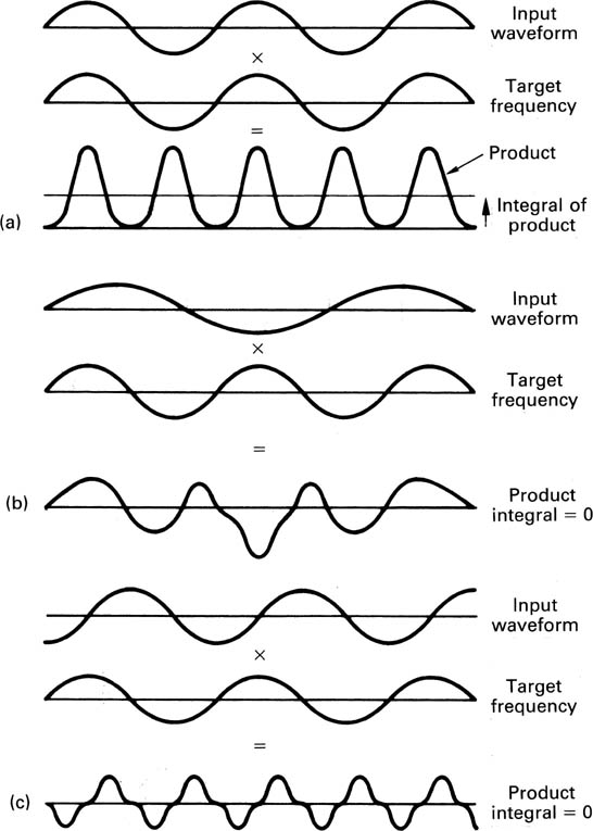
Figure 2.72(c) shows that the target frequency will not be detected if it is phase shifted 90° as the product of quadrature waveforms is always zero. Thus the discrete Fourier transform must make a further search for the target frequency using a cosine basis function. It follows from the arguments above that the relative proportions of the sine and cosine integrals reveal the phase of the input component. Thus each discrete frequency in the spectrum must be the result of a pair of quadrature searches.
Searching for one frequency at a time as above will result in a DFT, but only after considerable computation. However, a lot of the calculations are repeated many times over in different searches. The fast Fourier transform gives the same result with less computation by logically gathering together all the places where the same calculation is needed and making the calculation once.
2.24 The discrete cosine transform (DCT)
The DCT is a special case of a discrete Fourier transform in which the sine components of the coefficients have been eliminated leaving a single number. This is actually quite easy. Figure 2.73(a) shows a block of input samples to a transform process. By repeating the samples in a time-reversed order and performing a discrete Fourier transform on the double-length sample set a DCT is obtained. The effect of mirroring the input waveform is to turn it into an even function whose sine coefficients are all zero. The result can be understood by considering the effect of individually transforming the input block and the reversed block.
Figure 2.73 The DCT is obtained by mirroring the input block as shown at (a) prior to an FFT. The mirroring cancels out the sine components as at (b), leaving only cosine coefficients.
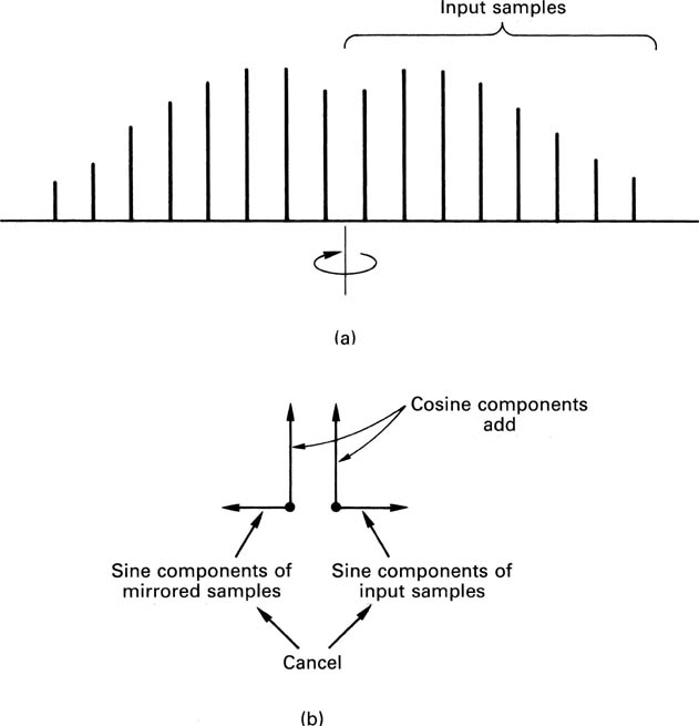
Figure 2.73(b) shows that the phase of all the components of one block are in the opposite sense to those in the other. This means that when the components are added to give the transform of the double length block all the sine components cancel out, leaving only the cosine coefficients, hence the name of the transform.6 In practice the sine component calculation is eliminated. Another advantage is that doubling the block length by mirroring doubles the frequency resolution, so that twice as many useful coefficients are produced. In fact a DCT produces as many useful coefficients as input samples.
For image processing two-dimensional transforms are needed. In this case for every horizontal frequency, a search is made for all possible vertical frequencies. A two-dimensional DCT is shown in Figure 2.74. The DCT is separable in that the two-dimensional DCT can be obtained by computing in each dimension separately. Fast DCT algorithms are available.7
Figure 2.74 The discrete cosine transform breaks up an image area into discrete frequencies in two dimensions. The lowest frequency can be seen here at the top left corner. Horizontal frequency increases to the right and vertical frequency increases downwards.
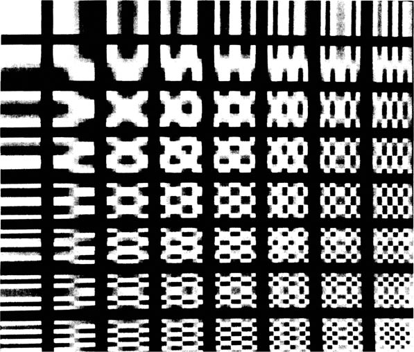
Figure 2.75 shows how a two-dimensional DCT is calculated by multiplying each pixel in the input block by terms which represent sampled cosine waves of various spatial frequencies. A given DCT coefficient is obtained when the result of multiplying every input pixel in the block is summed. Although most compression systems, including JPEG and MPEG, use square DCT blocks, this is not a necessity and rectangular DCT blocks are possible and are used in, for example, Digital Betacam and DVC.
Figure 2.75 A two-dimensional DCT is calculated as shown here. Starting with an input pixel block one calculation is necessary to find a value for each coefficient. After 64 calculations using different basis functions the coefficient block is complete.

The DCT is primarily used in MPEG-2 because it converts the input waveform into a form where redundancy can be easily detected and removed. More details of the DCT can be found in Chapter 5.
2.25 Modulo-n arithmetic
Conventional arithmetic which is in everyday use relates to the real world of counting actual objects, and to obtain correct answers the concepts of borrow and carry are necessary in the calculations.
There is an alternative type of arithmetic which has no borrow or carry which is known as modulo arithmetic. In modulo-n no number can exceed n. If it does, n or whole multiples of n are subtracted until it does not. Thus 25 modulo-16 is 9 and 12 modulo-5 is 2. The count shown in Figure 2.35 is from a four-bit device which overflows when it reaches 1111 because the carry out is ignored. If a number of clock pulses m are applied from the zero state, the state of the counter will be given by m Mod.16. Thus modulo arithmetic is appropriate to systems in which there is a fixed wordlength and this means that the range of values the system can have is restricted by that wordlength. A number range which is restricted in this way is called a finite field.
Modulo-2 is a numbering scheme which is used frequently in digital processes. Figure 2.76 shows that in modulo-2 the conventional addition and subtraction are replaced by the XOR function such that:
Figure 2.76 In modulo-2 calculations, there can be no carry or borrow operations and conventional addition and subtraction become identical. The XOR gate is a modulo-2 adder.

When multi-bit values are added Mod.2, each column is computed quite independently of any other. This makes Mod.2 circuitry very fast in operation as it is not necessary to wait for the carries from lower-order bits to ripple up to the high-order bits.
Modulo-2 arithmetic is not the same as conventional arithmetic and takes some getting used to. For example, adding something to itself in Mod.2 always gives the answer zero.
2.26 The Galois field
Figure 2.77 shows a simple circuit consisting of three D-type latches which are clocked simultaneously. They are connected in series to form a shift register. At (a) a feedback connection has been taken from the output to the input and the result is a ring counter where the bits contained will recirculate endlessly. At (b) one XOR gate is added so that the output is fed back to more than one stage. The result is known as a twisted-ring counter and it has some interesting properties. Whenever the circuit is clocked, the left-hand bit moves to the right-hand latch, the centre bit moves to the left-hand latch and the centre latch becomes the XOR of the two outer latches. The figure shows that whatever the starting condition of the three bits in the latches, the same state will always be reached again after seven clocks, except if zero is used. The states of the latches form an endless ring of non-sequential numbers called a Galois field after the French mathematical prodigy Evariste Galois who discovered them. The states of the circuit form a maximum length sequence because there are as many states as are permitted by the wordlength. As the states of the sequence have many of the characteristics of random numbers, yet are repeatable, the result can also be called a pseudorandom sequence (prs). As the all-zeros case is disallowed, the length of a maximum length sequence generated by a register of m bits cannot exceed (2m−1) states. The Galois field, however, includes the zero term. It is useful to explore the bizarre mathematics of Galois fields which use modulo-2 arithmetic. Familiarity with such manipulations is helpful when studying the error correction, particularly the Reed–Solomon codes used in recorders and treated in Chapter 6. They will also be found in processes which require pseudo-random numbers such as digital dither, considered in Chapter 3, and randomized channel codes used in, for example, DVB and discussed in Chapter 9.
Figure 2.77 The circuit shown is a twisted-ring counter which has an unusual feedback arrangement. Clocking the counter causes it to pass through a series of non-sequential values. See text for details.
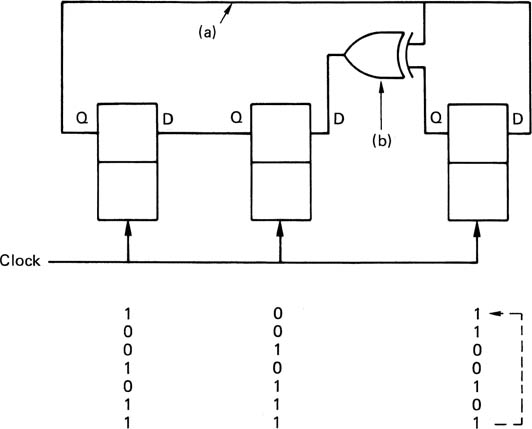
The circuit of Figure 2.77 can be considered as a counter and the four points shown will then be representing different powers of 2 from the MSB on the left to the LSB on the right. The feedback connection from the MSB to the other stages means that whenever the MSB becomes 1, two other powers are also forced to one so that the code of 1011 is generated.
Each state of the circuit can be described by combinations of powers of x, such as
The fact that three bits have the same state because they are connected together is represented by the Mod.2 equation:
Let x = a, which is a primitive element. Now
In modulo-2

In this way it can be seen that the complete set of elements of the Galois field can be expressed by successive powers of the primitive element. Note that the twisted-ring circuit of Figure 2.77 simply raises a to higher and higher powers as it is clocked. Thus the seemingly complex multibit changes caused by a single clock of the register become simple to calculate using the correct primitive and the appropriate power.
The numbers produced by the twisted-ring counter are not random; they are completely predictable if the equation is known. However, the sequences produced are sufficiently similar to random numbers that in many cases they will be useful. They are thus referred to as pseudo-random sequences. The feedback connection is chosen such that the expression it implements will not factorize. Otherwise a maximum-length sequence could not be generated because the circuit might sequence around one or other of the factors depending on the initial condition. A useful analogy is to compare the operation of a pair of meshed gears. If the gears have a number of teeth which is relatively prime, many revolutions are necessary to make the same pair of teeth touch again. If the number of teeth have a common multiple, far fewer turns are needed.
2.27 The phase-locked loop
All digital video systems need to be clocked at the appropriate rate in order to function properly. Whilst a clock may be obtained from a fixed-frequency oscillator such as a crystal, many operations in video require genlocking or synchronizing the clock to an external source. The phase-locked loop excels at this job, and many others, particularly in connection with recording and transmission.
In phase-locked loops, the oscillator can run at a range of frequencies according to the voltage applied to a control terminal. This is called a voltage-controlled oscillator or VCO. Figure 2.78 shows that the VCO is driven by a phase error measured between the output and some reference. The error changes the control voltage in such a way that the error is reduced, such that the output eventually has the same frequency as the reference. A low-pass filter is fitted in the control voltage path to prevent the loop becoming unstable. If a divider is placed between the VCO and the phase comparator, as in the figure, the VCO frequency can be made to be a multiple of the reference. This also has the effect of making the loop more heavily damped, so that it is less likely to change frequency if the input is irregular.
Figure 2.78 A phase-locked loop requires these components as a minimum. The filter in the control voltage serves to reduce clock jitter.

In digital video, the frequency multiplication of a phase-locked loop is extremely useful. Figure 2.79 shows how the 13.5 MHz clock of component digital video is obtained from the sync pulses of an analog reference by such a multiplication process.
Figure 2.79 In order to obtain 13.5 MHz from input syncs, a PLL with an appropriate division ratio is required.

Figure 2.80 shows the NLL or numerically locked loop. This is similar to a phase-locked loop, except that the two phases concerned are represented by the state of a binary number. The NLL is useful to generate a remote clock from a master. The state of a clock count in the master is periodically transmitted to the NLL which will re-create the same clock frequency. The technique is used in MPEG transport streams.
Figure 2.80 The numerically locked loop (NLL) is a digital version of the phase-locked loop.

References
1. Ray, S.F., Applied Photographic Optics, Chapter 17, Oxford: Focal Press (1988)
2. van den Enden, A.W.M. and Verhoeckx, N.A.M., Digital signal processing: theoretical background. Philips Tech. Rev. 42, 110–144, (1985)
3. McClellan, J.H., Parks, T.W. and Rabiner, L.R., A computer program for designing optimum FIR linear-phase digital filters. IEEE Trans. Audio and Electroacoustics, AU-21, 506–526 (1973)
4. Crochiere, R.E. and Rabiner, L.R., Interpolation and decimation of digital signals – a tutorial review. Proc. IEEE, 69, 300–331 (1981)
5. Rabiner, L.R., Digital techniques for changing the sampling rate of a signal. In B. Blesser, B. Locanthi and T.G. Stockham Jr (eds), Digitic Audio, pp. 79–89, New York: Audio Engineering Society (1982)
6. Kraniauskas, P., Transforms in Signals and Systems, Chapter 6, Wokingham: Addison-Wesley (1992)
7. Ahmed, N., Natarajan, T. and Rao, K., Discrete Cosine Transform. IEEE Trans. Computers, C-23, 90–93 (1974)