
CONTENTS
9.1 Noise–Linearity Trade-Off in Radio Design
9.3.1 Noise-Shaping, Blocker-Filtering Technique for Low Noise Integrated Receivers
9.3.2 Low Noise Gain Stage with Noise-Shaping Blocker Suppression
9.3.3 Current-Mode Noise-Shaped Filtering
9.4 Blixelter: Single-Stage Balun–LNA–Mixer–Filter Combo Topology
9.1 NOISE–LINEARITY TRADE-OFF IN RADIO DESIGN
Various wireless standards have emerged in recent years as a result of strong consumer demand for wireless applications [1,2]. The introduction of digital data communication with digital signal processing has fueled the development of numerous wireless standards and applications ranging from cellular, cordless phones and mobile TV to short range home RF, wireless LAN, and Bluetooth technologies.
While abundance of these wireless applications drives the technology to its limits to catch up with the demand, the crowding of the spectrum poses additional challenges for the designers. These emerging wireless standards have to be compatible with the existing standards. Hence, very strong interferers can coexist in the nearby channels, whereas the desired signal in the channel of interest might be very weak. As a result, the classical noise–linearity–power area trade-off becomes an even more pronounced challenge in wireless receiver design. Moreover, because of the trend to integrate multiple applications into a single wireless device, the battery life becomes an even more significant concern. Hence, any design solution for portable devices should offer low power operation. Since device size is also of greater concern in such portable devices, the designs should be reconfigurable for different frequency bands and applications to minimize the component count in the final design.
One of such emerging technologies, mobile TV, involves bringing TV services to mobile phones. It combines the services of a mobile phone with television content and represents a logical step for consumers, operators, and content providers. Mobile TV over cellular networks allows viewers to enjoy personalized, interactive TV with content specifically adapted to the mobile medium. The services and viewing experience of mobile TV over cellular networks differ in a variety of ways from traditional TV viewing. In addition to mobility, mobile TV delivers a variety of services, including video on demand.
Mobile TV is one of the most challenging wireless applications in terms of design requirements and specifications for the actual hardware designers. Once more, spread of numerous incompatible mobile TV standards across the globe could not be prevented, as was also the case with 2G and 3G mobile systems. These include digital video broadcasting-handheld (DVB-H), digital multimedia broadcasting (DMB), TDtv (based on TD-CDMA technology), 1seg (based on Japan’s integrated services digital broadcasting-terrestrial (ISDB-T)), digital audio broadcasting (DAB), and MediaFLO. None is ideal as all have drawbacks of one kind or another: spectral frequencies used or needed, signal strength required, new antennas and towers, network capacity. The main challenge now is the design of a universal multistandard receiver that is low cost and low power and can work over all the standards mentioned before. It is not only the variety of standards with different signal bandwidths and carrier frequencies that makes the design difficult to achieve but also the frequency band that every individual standard needs to cover. The frequency allocation for DVB-T/H system, for example, is shown in Figure 9.1. The DVB-T/H channels in the upper UHF band suffer from very strong nearby transmit-path GSM interferers residing at 880–915 MHz band. Due to strong antenna-to-antenna coupling in the devices accommodating both standards, the linearity requirement on the mobile TV receiver is very demanding because of the intermodulation (IM) products of the GSM interferers. Moreover, the DVB-T/H channels reside throughout most of the UHF band and part of the VHF band. Other analog and digital standards will continue to broadcast in these bands; hence, after the down-conversion, these adjacent blocker signals have to be filtered out with a sharp filter. The effect of intermodulation products is illustrated in Figure 9.2. The presence of strong adjacent channel blockers along with the desired signal at the baseband requires the design of a filter with high linearity and dynamic range. The filter must be able to process large signals with little intermodulation distortion. Harmonics of the signal will remain in the filter stopband, where they are automatically attenuated. However, it is very possible that third-order intermodulation between particular combinations of two tones in the stopband generates significant products in the passband as shown in Figure 9.2(a).
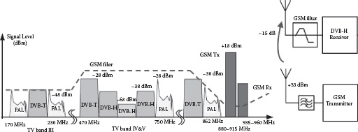
FIGURE 9.1 Frequency allocation plot for DVB-T/H.
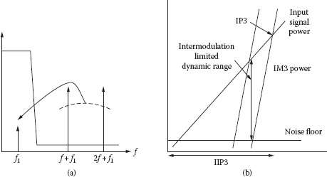
FIGURE 9.2 Intermodulation; (a) IM mixing due to nonlinearity, (b) implications of intermodulation on dynamic range.
A mobile TV receiver design for any of the mentioned standards must take the interferers into account. As a concrete example, ISDB-T, channel 7 in VHF band, overlaps with the National Television System Committee (NTSC) channel 8. Figure 9.3 illustrates this particular case. For the 3-Seg standard, the adjacent NTSC analog blocker channel can start as close as 300 kHz from the desired ISDB-T channel. Once more, the adjacent channel-filtering requirement is stringent. As a result, the receiver system design for mobile TV applications must consider not only power consumption and device size, but also multiple interferers that do exist in the same UHF and VHF bands. Moreover, mobility-dictated impairments, such as Doppler and multipath interference, set additional constraints for mobile TV receiver designers. Hence, new circuit architectures must be investigated to find receiver solutions for mobile TV technology that are low cost, low power, and high performance.

FIGURE 9.3 Channel allocation in 3-Seg (ISDB-T).
A typical direct conversion receiver (DCR) block diagram with corresponding signal and noise profiles is shown in Figure 9.4. The most critical block in the design is the first stage low noise amplifier (LNA), which generally sets the performance of the radio. In most cases, the gain of this first stage is set high, reducing the contribution of the following blocks to the overall system noise figure. In the case of nearby large blockers, though, linearity limitation in this block may dictate reduction in gain through a front-end AGC loop. Hence, the noise of the following stages will start to come into the picture. Thus, one should as well be careful in designing subsequent baseband blocks such as filters, variable-gain amplifiers (VGAs), analog-to-digital converters (ADCs), etc. As a result, one of the most important performance metrics for a radio is its sensitivity in environments with strong interferers.

FIGURE 9.4 Typical DCR receiver front end; (a) block diagram, (b) signal profile around the desired channel, (c) Noise profile around the desired channel.
The point immediately after RF down-conversion (“A” in the figure) is as well a critical point and determines the required circuitry down the chain depending on the signal and blocker profiles in the band of interest. A topology with a gain stage followed by filtering can again yield better sensitivity, as long as the blocker levels in the adjacent channels are limited and noise is the main factor to consider (Figure 9.5a). In the case of strong blockers, however, such architecture may not be optimum, due to the resulting stringent linearity requirement of the amplifier.
In the case of a gain-filtering interleaved architecture as shown in Figure 9.5(c), the design of the first amplifier stage can still be demanding. Thus, a filtering block might be required ahead of the gain stage as shown in Figure 9.5(b). The filter noise should be minimal for such a topology so as not to degrade the sensitivity due to noise. This can be satisfied with an additional cost of area and power in the filter if classical filter circuit topologies are to be employed [3–4,5,6,7,8,9,10,11].
The noise-canceling wideband CG-CS LNA topology of Figure 9.6 is utilized in the proposed work [12–13,14]. Features like noise-canceling, single-ended to differential conversion and relatively wideband input matching make this topology suitable for many UHF applications.

FIGURE 9.5 Noise–linearity trade-off in different architectures; (a) gain-filtering topology, (b) filtering-gain topology, (c) interleaved gain-filtering topology.

FIGURE 9.6 Noise-canceling LNA topology.
In this configuration, the noise generated in CG amplification device M1 is mirrored to the other CS amplification path and amplified. By simply matching the voltage gains through both paths, the noise of the device M1 can effectively be canceled. Hence, the main noise contributor remains M2, of which the noise can independently be optimized. The cascode devices M3 and M4 provide Miller isolation and gain boost in case the device output impedances are a limiting factor in the overall gain of the stage. Lb serves as an RF choke whose value sets the low frequency end of the gain characteristics.
As it has been pointed out in the previous sections, not only LNA noise but also the noise of mixers and other subsequent baseband blocks, in particular that of filters, may become a significant noise contributor in hostile spectrum conditions with strong blockers. This section is devoted to discussion of some noise-shaping analog baseband filtering techniques that can help to handle such interferers early along the chain and hence maintain a good sensitivity across a wide range of blocker profiles. The challenge in this, though, is to achieve this target without a significant impact on cost and power consumption.
9.3.1 NOISE-SHAPING, BLOCKER-FILTERING TECHNIQUE FOR LOW NOISE INTEGRATED RECEIVERS
The FDNR (frequency dependent negative resistance)-based filtering technique that is described in detail in this section offers unique advantages in terms of noise with its noise-shaping characteristics [15–16,17,18]. Moreover, the circuit provides this high-order filtering at the mixer output, protecting this node against blockers—a feature that traditional filter topologies cannot offer. Filtering at this critical node relaxes the mixer linearity spec and allows the mixer to have a higher gain. The input noise spec of postmixer blocks can thus be further relaxed. Hence, employing the technique in the receive chain of a radio can enhance the overall performance of the radio, an improvement that cannot be achieved using classical gain-filtering techniques unless area is sacrificed. The proposed technique, however, needs to be analyzed and the trade-offs should be clarified in terms of noise, linearity, power, area, and, most importantly, stability. Coexistence of multiple interdependent feedback paths dictates a careful analysis of the stability of the proposed circuit. To prove the clear benefits of the concept, detailed noise, linearity, and stability analysis are carried on in Section 9.3.1.1, Section 9.3.1.2, and Section 9.3.1.3, respectively. The details of the class-AB op-amp and the bandwidth calibration circuit are presented in Section 9.3.1.4. Section 9.3.1.5 presents the measurement results of a 65 nm CMOS (complementary metal oxide semiconductor) proof-of-concept test chip.
9.3.1.1 FDNR-Based Third-Order Elliptic Response Circuit
In the early 70s, following their invention, FDNRs were used extensively to realize high-order filter functions [19–20,21,22,23,24,25]. However, some known drawbacks encountered in the filter implementations have limited their use as a filter section. In most of the target low pass implementations, for example, there is a DC response associated with the series capacitor in the signal path [23]. The FDNR circuit satisfies the negative resistance function only in reference to the circuit ground. Moreover, the number of op-amps employed in an FDNR-based filter is greater than that of an integrator-based implementation of the same transfer function. Considering these disadvantages, these FDNR-based topologies have long been abandoned. The circuit of the proposed third-order section shown in Figure 9.7, however, offers some unique features that can be utilized to design a very low noise, blocker-immune radio baseband.
The main advantage of the proposed third-order configuration of Figure 9.7 is that it uses only one resistor in the signal path, the load resistor of the preceding stage Rf, to realize the desired filter transfer function. Hence, the load resistance of a mixer or of a gm stage can be reutilized as a part of the filter transfer function, which is not the case for classical filter topologies. The noise contribution of this particular resistor is already accounted for in the mixer noise budget and the noise of the FDNR resistors R1, R2, and R3 is shaped. Since the op-amps are not in the signal path, their flicker noise contributions are also shaped and hence contribute less to the overall filter noise.
Moreover, as opposed to classic filter topologies, the op-amps of the proposed third-order section are not in the signal path and hence do not contribute any IQ mismatch or DC offset, which is a much desired property in a receiver chain. The signal transfer function of this circuit from input to output can be written as follows:
(9.1) |
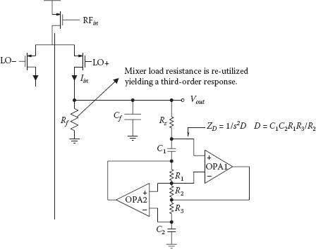
FIGURE 9.7 Simplified single-ended schematic of the proposed third-order elliptic circuit at the mixer output.
(9.2) |
This signal transfer function provides a notch at a frequency,
and the notch frequency depends on the value of D and Rz. As a result, a large variety of component values can be used to realize the desired cutoff and notch frequencies. Linearity, stability, and area trade-offs associated with the proposed circuit will be investigated to narrow down to an optimum component value combination for the target application.
The schematic including the noise sources in an FDNR is shown in Figure 9.8. In the proposed circuit, the noise of all passive and active components in the FDNR section—namely, of Rz, R1, R2, R3, OPA1, and OPA2—is shaped. Hence, the only substantial noise contributor is Rf, whose noise contribution is accounted for in the amplifier or mixer noise budget.
In order to clarify the noise-shaping concept of the proposed circuit, the noise transfer functions from each of these contributors have been calculated and presented as follows:

FIGURE 9.8 Schematic including the noise sources in the circuit.
The OPA1 noise transfer function is
(9.3) |
The OPA2 noise transfer function is
(9.4) |
The Rz noise transfer function is
(9.5) |
The R1 noise transfer function is
(9.6) |
The R2 noise transfer function is
(9.7) |
The R3 noise transfer function is
(9.8) |
Figure 9.9 shows the plots for the magnitude of these noise transfer functions as well as the signal transfer function. Since the noise generated by the FDNR resistors is shaped, the designer can use larger resistors (noisier) and hence can reduce the capacitor size. This results in a significant area saving. As a means of comparison, the total amount of capacitor required versus the desired noise level in a bandwidth of 1 MHz is plotted in Figure 9.10 for various third-order filter topologies (Figure 9.11) as well as the FDNR-based filter topology described in this work. It should be noted that the single op-amp topologies (Sallen-Key and multiple feedback) cannot achieve an elliptic response; hence, their overall figure of merit may not be as high for applications requiring large attenuation in the nearby channels.
For the sake of simplicity, the plots shown in Figure 9.10 reflect the noise due only to the resistors in the circuits and do not include the noise contributions of the op-amps used in these circuits. Since the noise of the op-amps is also shaped in an FDNR-based topology, the advantage of this topology becomes even more pronounced once the op-amp noise contributions are also included in the analysis.

FIGURE 9.9 Signal and noise transfer functions of the proposed circuit.

FIGURE 9.10 Total integrated in-band noise versus required capacitance for the various third-order filter topologies shown in Figure 9.11.
There are two important cases that need to be addressed regarding the linearity of the circuit. The first is the response of the circuit to two strong tones at the blocker frequencies. The IM3 product of these tones is minimized by providing a very large gain in the op-amps at these blocker frequencies. The other case is the nonlinearity experienced by the in-band signal. Depending on the ratio of notch frequency to cutoff frequency, the overall filter response can display some peaking around the cutoff frequency. The peaking in the signal transfer function might result in larger peaking at the internal FDNR nodes, particularly at the operational amplifier (op-amp) outputs of the proposed circuit. Thus, a full swing in-band signal might cause the FDNR op-amps outputs to have even a larger swing degrading the overall linearity of the circuit. Hence, the signal transfer function should be optimized, taking the peaking at the internal FDNR nodes into account.
The transfer function from input to op-amp2 output can be written as follows:
(9.9) |
The magnitudes of this transfer function as well as the signal transfer function are shown in Figure 9.12(b) and Figure 9.12(a), respectively, for range filter characteristics corresponding to the same cutoff and notch frequencies. As can be observed from the plots, more rapidly decreasing filter response with more stopband attenuation results in more peaking at the internal nodes. We can approximate the magnitude of the transfer function given in (9.9) around the cutoff frequency as follows:

FIGURE 9.11 Integrated in-band noise for various third-order filter topologies; (a) Sallen-Key, (b) leap-frog (ladder), (c) multiple-feedback, (d) Tow-Thomas.
(9.10) |
Equation (9.10) suggests that the only way to obtain higher attenuation for fixed cutoff and notch frequencies without introducing extra peaking is to increase the value of the capacitor, C1. The amount of peaking that is allowed at the op-amp output sets the minimum value for this capacitor, as shown in Figure 9.13.

FIGURE 9.12 (a) The filter response for various peaking levels; (b) corresponding peaking levels at the FDNR internal node.
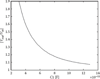
FIGURE 9.13 Minimum C1 capacitance values corresponding to various peaking levels at the op-amp outputs.
The stability of the system should also be taken into account while optimizing the design for the desired filter response. There are multiple feedback networks that require attention. A simplified stability analysis of the system is useful since it has implications on unity gain bandwidth, DC gain, and compensation scheme of the op-amps used in the design. In order to simplify the analysis, one of the op-amps is considered to be ideal while the other one is analyzed with the network around it. If each of these independent cases provides the required margin for stability, the initial assumption for each individual case is not violated, and hence the system can be expected to be stable.
Figure 9.14(a) shows the loop around OPA1. In order to simplify the analysis, the same capacitor and resistor values are used for all of the components in the circuit. Switching to the actual design parameters would only move the poles and zeros around the ones corresponding to this simplified configuration. The loop transfer function around this op-amp can be written as follows:
(9.11) |
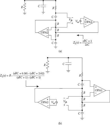
FIGURE 9.14 (a) Stability case for OPA1, where OPA2 is assumed to be ideal; (b) stability case for OPA2, where OPA1 is assumed to be ideal.
where A(s) is the op-amp transfer function when loaded with an impedance
This loading corresponds to a pole and a zero in the op-amp transfer function including the output impedance of the driver devices in the op-amp. All poles and zeros are in the vicinity of the filter cutoff and notch frequency and all cancel out, including the ones resulting from the op-amp loading. However, two of the zeros in the loop transfer function are complex conjugate and cause a notch in both the amplitude and phase response. If the gain of the amplifier around this notch frequency is not large enough to absorb the phase and amplitude notch with margin, system stability can be threatened. The loop transfer function is the same for the OPA2 case shown in Figure 9.14(b). However, this time the load seen by the op-amp is
and has two poles and two zeros. Again, the second op-amp, OPA2, needs to be able to provide sufficient gain around the cutoff frequency.
In conclusion, the op-amps in the proposed design not only should target high unity gain bandwidth, but also should provide a large gain around the desired notch frequency. This is generally the case for most of the op-amps used in filter applications but, for this particular FDNR application, this requirement has an impact on the stability of the system.
9.3.1.5 Op-amp and Bandwidth Calibration Circuit
The schematic of the op-amp used in the design is shown in Figure 9.15(a). This folded-cascode op-amp achieves a unity gain bandwidth greater than 200 MHz, consuming 380 μA from a 1.2 V supply with a phase margin of 61°. The input devices M1 and M2 are native (zero-Vt) devices to allow a rail-to-rail input swing. The PMOS and NMOS cascode devices are biased with a Vt-multiplier bias stage shown in Figure 9.15(a). Hence, the cascode bias points track the process variations, adjusting the headroom in these devices accordingly. The output is a class-AB stage with cascode devices biasing the floating current sources. This way, high impedance is maintained at the first stage output. Higher impedance at this node results in a higher unity gain bandwidth since the total amount of compensation capacitor needed drops with higher impedance at this node.
The bandwidth calibration circuit used in the design is shown in Figure 9.16(b). During the initial calibration a 7-bit bandwidth calibration code sets the resistive DAC targeting the desired filter bandwidth for a given crystal clock frequency. The trim range of this resistor is large enough to cover the whole filter bandwidth as well as any crystal frequency in the range of 10 to 40 MHz that is used as a reference. Following this, successive approximation logic computes a calibration code with the help of a comparator, as illustrated in Figure 9.16(b). Note that, since the resistor in this configuration is used as a trim element determining the bandwidth and crystal frequency, the capacitor is used as the calibration element with 6-bit resolution. In the filter side, in addition to a corresponding 6-bit resolution capacitor bank, there is a resistor trim to switch between the high end and the low end of the band. Tuning resolution at the low band mode is around 20 kHz.

FIGURE 9.15 (a) The native input, folded-cascode, class-AB op-amp schematic; (b) bandwidth calibration circuit.
9.3.1.6 Measurements
A design covering a tuning range from 700 kHz to 5.2 MHz is fabricated in a 65 nm CMOS process and tested. The cutoff, notch, and stop-band characteristics can independently be set to satisfy the blocker and noise requirements of various applications across the band with a 7-bit control word corresponding to a tuning resolution of 20 kHz. Figure 9.16(a) shows various filter transfer function curves corresponding to different trim codes across the band. The testing and characterization are done for two distinct applications, integrated services digital broadcasting-terrestrial (ISDB-T) and digital video broadcasting-handheld (DVB-H), with signal bandwidths of 750 kHz and 3.8 MHz, respectively. The filter can be tuned to provide optimum response for in-band and blocker signals corresponding to these two example applications (Figure 9.16b). In ISDB-T mode, the signal cutoff is around 750 kHz whereas the N + 1 blocker starts at 2.5 MHz. In DVB-H mode, the signal bandwidth is around 3.8 MHz, whereas the N + 1 blocker power can occur in the next 8 MHz bandwidth. The optimum case for the DVB-H has a slight peaking in the filter response, since the notch frequency is set to be relatively close to filter cutoff.

FIGURE 9.16 (a) Measured filter response for various bandwidth settings across the band; (b) filter responses corresponding to target ISDB-T and DVB-H applications.
The noise characteristics of the filter for these target bands are shown in Figure 9.17. Figure 9.17(a) shows the noise in ISDB-T mode, whereas Figure 9.17(b) shows the noise in DVB-H mode. The expected noise shaping can clearly be observed for both cases. The noise density in the signal band is around 7.5 nV/sqrtHz, which is mainly due to the 2 kΩ output resistance (Rf) of the driving stage. The 20 dB/decade in-band noise roll-off stops once the noise level of this resistor is reached. This resistor is the load resistance of the mixer or the driving stage and its noise contribution is already accounted for. It is important to note that this load resistor cannot be utilized in other active filter topologies and hence additional resistors are required in the filter to achieve the desired filter characteristic. This is a unique advantage of the proposed FDNR-based topology. With regard to linearity, HD tests and two-tone IM3 tests were conducted for both target modes. Figure 9.18(a) shows that a 250 KHz, 420 mVpp differential tone in ISDB-T mode results in –57 dB HD2. A differential tone of 1.2 MHz, 420 mVpp in DVB-H mode yields –59 dB HD2 (Figure 9.18b).
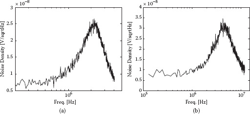
FIGURE 9.17 (a) Filter noise in ISDB-T mode; (b) filter noise in DVB-H mode.
In ISDB-T mode, 2.4 and 4.4 MHz blockers (420 mVpp differential each) result in –80.4 dBc IM3, which corresponds to an out-of-band IIP3 of 36.5 dBm (Figure 9.19a). In-band IIP3 for this case is 22.5 dBm. In DVB-H mode, 5 and 8 MHz blockers (420 mVpp differential each) result in –69.8 dBc IM3, which corresponds to an outof-band IIP3 of 31.5 dBm (Figure 9.19b). In-band IIP3 for this case is 20 dBm. For both cases, the tones are swept in-band and out-of-band recording the IIP3 for each of these cases. The plots showing IIP3 with varying average two-tone frequency are shown in Figure 9.20. The design occupies a die area of 0.16 mm2 in the mentioned 65 nm CMOS process. Total power consumption is in the range of 2 to 3.2 mA from a 1.2 V supply, depending on the received signal strength.

FIGURE 9.18 (a) In-band HD in ISDB-T mode; (b) in-band HD in DVB-H mode.

FIGURE 9.19 (a) Two-tone test in ISDB-T mode; (b) two-tone test in DVB-H mode.
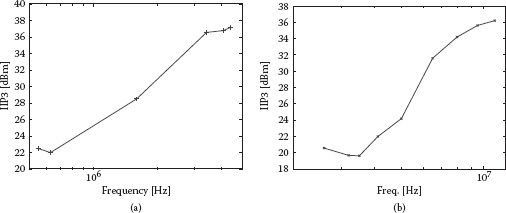
FIGURE 9.20 (a) IIP3 versus freq. sweep in ISDB-T mode; (b) IIP3 versus freq. sweep in DVB-H mode.
The technique enhances the sensitivity of a receiver chain significantly, particularly in an environment where strong blockers can coexist. Performance metrics of a 65 nm CMOS test chip are summarized in Table 9.1. Comparison of the literature in terms of noise and required capacitance per pole is shown in Figure 9.21. It can be seen that the approach proposed in this work results in lower noise for a given amount of capacitance relative to published work to date. The die photo of the design is shown in Figure 9.22.
9.3.2 LOW NOISE GAIN STAGE WITH NOISE-SHAPING BLOCKER SUPPRESSION
In this section, a blocker-aware gain stage is presented. The asymmetric floating frequency dependent negative resistance (AFFDNR) circuit in the feedback of an amplifier is introduced as a unique solution for providing gain in the signal band while simultaneously implementing a third-order, low pass elliptic response for the blocker signals. Due to its noise-shaping characteristics, the noise contribution due to the filtering action is insignificant.
The technique proposed in this section offers a solution with simultaneous gain and noise-shaping filtering—namely, amplification only in the band of interest. Low noise amplification of only the desired signal is proposed against the classical approach of amplifying everything, including the blockers, and then trying to filter out the blockers in the subsequent filtering stage. Avoiding the amplification of the blockers not only relaxes the linearity spec of the amplifier, but also relieves the filtering requirements of the following filtering stage.
9.3.2.1 AFFDNR-Based Gain Stage
A new circuit topology based on the previously mentioned FDNR structure, the AFFDNR used in the feedback of a programmable gain amplifier (PGA) is shown in Figure 9.23. Figure 9.23(a) shows an instrumentation topology with high input impedance, while Figure 9.23(b) shows a fully differential implementation with finite input impedance. Two single-ended op-amps are used in instrumentation topology, whereas, one fully differential op-amp with common mode feedback is used in the fully differential case.
TABLE 9.1
Performance Summary of the Proposed Baseband Prefilter
Technology |
65 nm CMOS |
Die area |
0.24 mm2 |
Power supply |
1.2 V |
Current consumption |
|
Max |
3.2 mA |
Min |
2 mA |
DC-gain |
0 dB |
fc |
|
ISDB-T mode |
750 kHz |
DVB-H mode |
3.8 MHz |
Out-of-band IIP2 |
|
ISDB-T mode |
57 dBm |
DVB-H mode |
50.5 dBm |
Tuning range |
700 kHz–5.2 MHz |
Tuning resolution |
3% |
Noise density |
7.5 nV/sqrtHz |
SFDR |
|
ISDB-T mode |
84 dB |
DVB-H mode |
76.6 dB |
DR (at HD3 = 40 dB) |
|
ISDB-T mode |
92.7 dB |
DVB-H mode |
85.5 dB |
In-band IIP3 |
|
ISDB-T |
22.5 dBm |
f1 = 500 kHz, f2 = 600 kHz |
|
DVB-H |
20 dBm |
f1 = 2.4 MHz, f2 = 2.8 MHz |
20 dBm |
Out-of-band IIP3 |
|
ISDB-T |
36.5 dBm |
f1 = 2.4 MHz, f2 = 4.4 MHz |
|
DVB-H |
31.5 dBm |
f1 = 5 MHz, f2 = 8 MHz |
|
In-band HD2 |
|
(420 mVpp diff.) |
|
ISDB-T(f = 500 kHz) |
−57 dB |
DVB-H(f = 1.2 MHz) |
−59 dB |
The PGA op-amp input stage should be able to handle signal swing in the instrumentation topology, while in the fully differential case, the op-amp inputs are at virtual ground and do not experience any voltage swing. The circuits are composed of the main PGA op-amps that realize the gain with the use of the feedback resistance Rf and input resistance Rin. Although linearity of such a system is relaxed, allowing larger gain in the amplifier, certain applications still require gain variability depending on the received signal strength. Input resistor Rin can be trimmed for PGA operation if gain variation is desired. The filtering stage is placed in the feedback path in parallel with Rf. Rf is incorporated into the filter transfer function and hence serves a dual function: providing gain and adding filtering. When the signal is applied to the input terminal, the feedback path with AFFDNR presents an impedance of Rf for the in-band signal, whereas the blocker sees a short to the output. The blocker signals do not experience any gain in the signal path. Thus, the linearity spec of the amplifier is relaxed since the output cannot see a large blocker voltage swing. More precisely, the signal in the desired channel of interest is amplified with a third-order elliptic filter characteristic due to the proposed frequency selective feedback. It should be noted that the proposed AFFDNR is not a reciprocal circuit and the mentioned filtering action can only be obtained provided that the polarity is as shown in Figure 9.23(b). Namely, the impedance looking into the node A, ZA is desired negative resistance, whereas the impedance looking into the node B, ZB is inductive when the opposing port is grounded for each of the cases. In this topology, the AFFDNR filter amplifiers are not in the signal path, so no additional DC offset or IQ imbalance is introduced as opposed to common amplifier-filter topologies.

FIGURE 9.21 Literature comparison in terms of noise and required capacitance per pole.

FIGURE 9.22 Die microphotograph of the design.

FIGURE 9.23 Amplifiers with AFFDNR feedback; (a) instrumentation topology, (b) fully differential implementation.
Using KVL and KCL, the equation defining the relation between the input and output of this AFFDNR feedback circuit can be written as
(9.12) |
where F(s) is the transmission function and
(9.13) |
Looking into the relation between input and output provided in (9.12), for the low frequency in-band signals, F(s) is unity and hence an in-band signal experiences expected noninverting gain of
The input–output relation around the notch frequency, however, yields an interesting case. One would expect a minimum gain of unity from this amplifier topology—worst case being the zero feedback impedance. Looking into the response of the amplifier around the notch frequency, however, we can even observe some attenuation (Figure 9.26). The reason for this becomes clear once the F(s) in (9.12) is analyzed. Figure 9.24 shows the bode plot of the function F(s). The phase response reaches 180° very quickly, while the amplitude response is in the ramp-up and still has a relatively finite value. Such a finite magnitude with a negative sign corresponds to attenuation in the overall signal transfer function given in (9.12).
9.3.2.2 Noise Analysis
The detailed schematic of the simplified single-ended design including the noise sources is shown in Figure 9.25. The noise of the amplifier elements, the input resistance Rin and the feedback gain resistor Rf, remains the same and sets the noise floor for this topology. The noise of the AFFDNR filtering section elements (Rz, R1, R2, R3, OPA1, and OPA2) is, however, shaped and does not contribute to the overall noise figure significantly. Thus, one can obtain a relative high-order filtering without extra noise penalty. To demonstrate the noise-shaping concept of the proposed circuit explicitly, the noise transfer functions from each of these contributors to the output have been calculated and are as follows.

FIGURE 9.24 Bode plot for the function F(s) given in Equation (9.12).
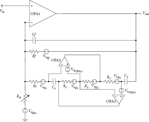
FIGURE 9.25 Schematic of a simplified single-ended circuit including the noise sources.
The OPA2 noise transfer function is
(9.14) |
The OPA3 noise transfer function is
(9.15) |
The Rz noise transfer function is
(9.16) |
The R1 noise transfer function is
(9.17) |
The R2 noise transfer function is
(9.18) |
The R3 noise transfer function is
(9.19) |
The signal transfer function from input to output can be written as follows:
(9.20) |
Figure 9.26 shows the plots for the magnitude of these noise transfer functions as well as the signal transfer function.
It is also possible to use the noise-shaping characteristic of the proposed technique to reduce overall chip area. Since the noise generated by the AFFDNR resistors is shaped, this enables the designer to use larger resistors (noisier) and hence reduce the capacitor size. This approach can result in significant area saving for a particular noise level. As a means of comparison, the total amount of capacitor required versus the desired in-band input referred noise level is plotted in Figure 9.27 for various third-order filter topologies as well as the circuit topology described in this work.

FIGURE 9.26 Signal and noise transfer functions showing the noise shaping.

FIGURE 9.27 Desired noise level versus required capacitor value for a range of filter topologies targeting the same cutoff frequency of around 3.5 MHz.
9.3.2.3 Measurement Results
A differential instrumentation stage covering a frequency range from 700 kHz to 4.2 MHz is fabricated in a 65 nm CMOS process and tested (Figure 9.28). The cutoff, notch, and stop-band characteristics can independently be set to satisfy the blocker and noise requirements of various applications across the band with a 7-bit control word corresponding to a tuning resolution of 20 kHz. The design consumes a die area of 0.12 mm2 and the total power consumption is in the range of 3 to 4.8 mA from a 1.2 V supply, depending on the received signal strength. Figure 9.29(a) shows various amplifier transfer function curves corresponding to different trim codes across the band.

FIGURE 9.28 (a) Fully differential cascade topology; (b) cascade instrumentation topology.
The testing and characterization is done for ISDB-T and DVB-H, with signal bandwidths of 750 kHz and 3.8 MHz, respectively. The radio chain employing the circuit requires that IM3 levels resulting from –3.5 dBm N + 1 blockers be below –70 and –60 dBc for ISDB-T and DVB-H modes, respectively. The input referred noise requirements are 12 and 9 nV/sqrtHz for ISDB-T and DVB-H modes, respectively. The transfer characteristics with various gain steps corresponding to these target applications are shown in Figure 9.29(b). In ISDB-T mode, the signal cutoff is around 750 kHz, whereas the N + 1 blocker is centered around 2.5 MHz. In DVB-H mode, the signal bandwidth is around 3.8 MHz, whereas the N + 1 blocker power can occur in the next 8 MHz bandwidth. The optimum case for the DVB-H has a slight peaking in the filter response, since the notch frequency is set to be relatively close to filter cutoff.

FIGURE 9.29 (a) Measured amplifier bandwidth characteristics across the band; (b) amplifier response for various gain settings in ISDB-T and DVB-H modes.
Regarding the noise budget allocation, setting the noise contribution of the AFFDNR and of the gain amplifier is not the optimum choice since the power is more of a concern in the amplifier design. An optimum design strategy for the target design was to allocate most of the in-band noise budget to the amplifier to reduce its power consumption and limit the FDNR contributions. The noise characteristics of the filter for these target bands are shown in Figure 9.30. Figure 9.30(a) shows the noise in ISDB-T mode, whereas Figure 9.30(b) shows the noise in DVB-H mode. It can be observed from these plots that the shaped AFFDNR contribution becomes dominant only at the edge of the band. The measured noise density in the signal band is around 9.5 nV/sqrtHz in DVB-H mode and 14 nV/sqrtHz in the ISDB-T mode. Total capacitance required in the design corresponding to these noise levels was 120 pF.
With regard to linearity, HD tests and two-tone IM3 tests were conducted for both target modes. Figure 9.31(a) shows that a 250 kHz, 750 mVpp differential tone at the output in ISDB-T mode results in –57.4 dB HD2 and –58.9 dB HD3. In DVB-H mode a 1.2 MHz, 750 mVpp differential tone at the output yields –60 dB HD2 and –57 dB HD3 (Figure 9.31b).
In ISDB-T mode, 2.25 and 3.75 MHz blockers (420 mVpp differential each) result in –78 dBm IM3 at the output, which corresponds to an out-of-band IIP3 of 37 dBm (Figure 9.32a). In DVB-H mode, 7 and 11 MHz blockers (420 mVpp differential each) result in –65.6 dBm IM3 at the output, which corresponds to an out-of-band IIP3 of 29.7 dBm (Figure 9.32b). In Figure 9.33, measured IIP3 interpolation plots are presented for both target bands. Moreover, the tones are swept across the blocker band recording the IIP3 for each of these cases. The plots showing IIP3 with varying average two-tone frequency are shown in Figure 9.34.

FIGURE 9.30 Total input referred noise measured; (a) in ISDB-T mode, (b) in DVB-H mode.
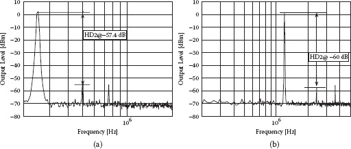
FIGURE 9.31 In-band distortion levels measured; (a) in ISDB-T mode, (b) in DVB-H mode.

FIGURE 9.32 Two-tone tests; (a) output spectrum for 240 mVpp diff. each, 2.25 MHz and 3.75 MHz input blockers in ISDB-T mode; (b) output spectrum for 240 mVpp diff. each, 7 MHz and 11 MHz input blockers in DVB-H mode.

FIGURE 9.33 Measured IIP3; (a) in ISDB-T mode, (b) in DVB-H mode.
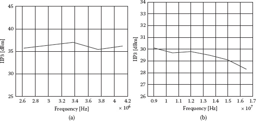
FIGURE 9.34 IIP3 across the blocker band; (a) in ISDB-T mode, (b) in DVB-H mode.
Performance metrics of this test circuit are summarized in Table 9.2. The die picture is shown in Figure 9.35.

FIGURE 9.35 Die microphotograph of the PMA.
TABLE 9.2
Performance Summary of the Proposed Baseband PMA
Technology |
65 nm CMOS |
Die area |
0.13 mm2 |
Power supply |
1.2 V |
Current consumption |
|
Max |
4.8 mA |
Min |
3 mA |
Gain settings |
|
fc |
|
ISDB-T mode |
750 kHz |
DVB-H mode |
3.8 MHz |
Out-of-band IIP2 |
|
ISDB-T mode |
75 dB |
DVB-H mode |
65.5 dB |
Tuning range |
700 kHz–4.2 MHz |
Tuning resolution |
3% |
Noise density |
|
ISDB-T mode |
14 nV/sqrtHz |
DVB-H mode |
9.5 nV/sqrtHz |
DR (at HD3 = 40 dB) |
|
ISDB-T mode |
87.6 dB |
DVB-H mode |
83.3 dB |
Out-band IIP3 |
|
ISDB-T |
37 dBm |
f1 = 2.25 MHz, f2 = 3.75 MHz |
|
DVB-H |
29.7 dBm |
f1 = 7 MHz, f2 = 11 MHz |
|
HD2 (750 m Vpp diff.) |
|
ISDB-T (f = 500 kHz) |
−57.4 dB |
DVB-H (f = 1.2 MHz) |
−60.5 dB |
Total cap size |
120 pF |
9.3.3 CURRENT-MODE NOISE-SHAPED FILTERING
Current-mode noise-shaping filtering has as well been proven to another low noise, low distortion filtering technique that is suitable for wireless communication applications. The circuit converts a simple gm-C type of cascade into a more effective second-order filter with complex poles by uniquely cross coupling the intermediate nodes intp and intn (Figure 9.36) [26]. Intuitively, device noise is pushed back at low frequencies while it finds a low impedance path into the capacitors at high frequencies and hence gains up at the load. Assuming the same gm for all of the active MOS devices, the filter response can be written as follows:
(9.21) |
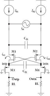
FIGURE 9.36 Detailed circuit schematic of a current-mode filter.
Again, the same outstanding feature in this noise-shaping filter as in the case of FDNR-based ones is that the blocker currents are not allowed to reach high impedance nodes without filtering. Figure 9.37 shows the filter transfer function as well as the output noise profile.

FIGURE 9.37 Filter gain response and noise characteristics across the channel.
9.4 BLIXELTER: SINGLE-STAGE BALUN–LNA–MIXER–FILTER COMBO TOPOLOGY
The circuit technique that is introduced in this section provides balun, LNA, mixer, and noise-shaped filter functions all in one folded circuit stage as shown in Figure 9.38. In this architecture, using minimal numbers of transistors and achieving a high gain and high-order filtering stage results in a low noise, high-sensitivity receiver in the existence of strong adjacent in-band blockers as well as other outof-band interferers. In this topology, which is referred to as Blixelter, the RF input drives the noise-canceling LNA device pair M10 and M11. This common-gate, common-source amplifier pair as well provides balun functionality, converting the single-ended signal to differential. LO clock source mixes the RF signal down through mixer devices M12 through M15. A larger portion of the LNA device currents are provided through ILNA current sources and hence do not flow through the mixers, reducing the mixer noise contribution. Current source ILNA thermal noise can be limited and its flicker noise contribution is upconverted and hence will not fall in-band. The current sources Ib1 and Ib2 provide DC bias current for the front-end LNA–mixer pair and some remaining current flows through M6 and M7, biasing the folded filter section. This section implements a second-order pipe filter through Cf1 and Cf2 and additional third-order notch filtering at the load through FDNR and Cx. Since both of these techniques provide noise-shaped filtering, the strong interferers at the adjacent channels are attenuated without significant addition of filter noise in-band. The current sources Ib1 and Ib2 remain significant flicker noise contributors and hence they occupy a relatively large die area not to degrade noise at the lower end of the channel band. The receiver front ends implementing such topology can allow higher gain without suffering from adjacent interferers and hence can achieve better sensitivity for a given current and area budget. The detailed schematic of the FDNR section is shown in Figure 9.39. The overall filter transfer function for the combiner section can be written as
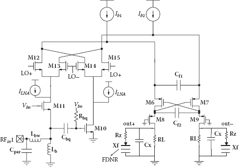
FIGURE 9.38 Detailed circuit schematic of Blixelter.
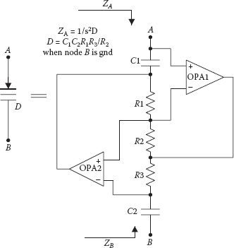
FIGURE 9.39 FDNR detailed circuit schematic.
(9.22) |
where
of FDNR and gm is the transconductance for the devices M6 through M9. The filter capacitors Cx and C2, which are shown to be single ended conceptually here in the schematic, are implemented fully differential in the actual design.
The simulated frequency response and noise characteristics of the folded filtering section in a 28 nm CMOS process are shown in Figure 9.40 for a 5 MHz DVBH channel. An average attenuation of 30 dB is achieved immediately at the adjacent channel with the notch corresponding to the center of the adjacent channel at around 8 MHz. This amount of filtering is achieved with less than 10 nV/sqrtHz average noise density in-band corresponding to a total of 150 pF capacitor area.
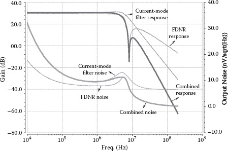
FIGURE 9.40 Noise and frequency response of the folded filtering section.
At the input of the proposed front end, a 1 uH RF choke is used, providing a wideband matching down to VHF frequencies. S11 across the whole UHF band is better than –25 dB in simulations assuming 0.8 nH bondwire inductance and 0.5 pF ESD and package parasitics (Figure 9.41).
The simulated conversion gain of the Blixelter front end is 26.8 dB for a UHF DVBH channel at 470 MHz with adjacent blocker IIP3 of –11.48 dBm, which corresponds to an effective out-of-band OIP3 of 15.32 dBm (Figure 9.42 and Figure 9.43). The tones for this analysis were chosen at the center of the immediate adjacent channel, at 2.5 and 3.5 MHz away from the 5 MHz channel edge. The notch response around the desired channel is visible at around the carrier frequency of 470 MHz in Figure 9.42.

FIGURE 9.41 Simulated S11 of the Blixelter front end.
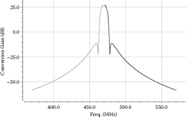
FIGURE 9.42 Simulated conversion gain around 470 MHz UHF channel.
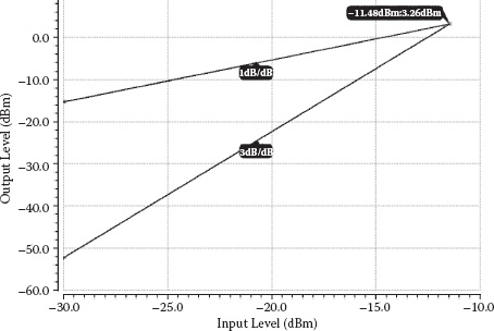
FIGURE 9.43 Adjacent blocker channel linearity.
Finally, the noise figure plot of the proposed Blixelter front end is shown in Figure 9.44. The NF across the channel is around 10.8 dB. The value goes up due to noise-shaping, reaching 11 dB at the high end of the band at 5 MHz. The value deteriorates to 14 dB at the flicker-noise dominant frequencies below 200 kHz. The total current consumption of the proposed circuit is 10.4 mA from a 1.8 V supply.
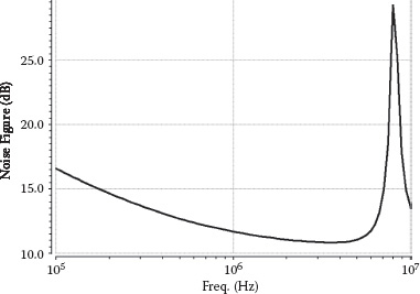
FIGURE 9.44 Blixelter noise figure.
In conclusion, with an increasing demand for wireless/mobile applications, deep, submicron CMOS has become a very attractive platform to design SOC radios for the emerging standards. Although it has indisputable dominance for such applications due to the amount of DSP that can be integrated, CMOS poses significant noise and linearity challenges to the front-end designers, for it has low supply voltage requirements. Due to rapid spectrum crowding and demand for increased communication range, this historic noise–linearity–power trade-off is pronounced even more. This chapter has presented some noise-shaping, noise-canceling techniques at front end and baseband, focusing particularly on FDNR-based noise-shaping filtering techniques in a 65 nm CMOS process. Finally, all of the techniques presented are combined, forming what is called “Blixelter,” which includes balun, LNA, mixer, and high-order noise-shaped filter functionalities in one single folded circuit stage. Implementing fifth-order noise-shaped filtering, all in current domain, helps to attenuate nearby blockers before they can reach the LNA–mixer load. Thus, the topology not only eliminates the need for a complex front-end AGC loop, but also relaxes the noise–linearity specification of the subsequent baseband blocks.
1. P. Chaudhury et al., The 3GPP proposal for IMT-2000. IEEE Communications Magazine, vol. 37, pp. 71–81, Dec. 1999.
2. M. Zeng et al., Recent advance in wireless communications. IEEE Communications Magazine, vol. 37, pp. 128–138, Sept. 1999.
3. J. F. Fernandez-Bootello et al., A 0.18 μm CMOS low-noise elliptic low-pass continuous-time filter. Proceedings of IEEE International Symposium on Circuits and Systems, pp. 800–803; vol. 1, 23–26 May 2005.
4. A. Yoshizawa et al., A channel-select filter with agile blocker detection and adaptive power dissipation. IEEE Journal of Solid-State Circuits, vol. 42, no. 5, pp. 1090–1099, May 2007.
5. C. H. J. Mensink et al., A CMOS soft-switched transconductor and its application in gain control and filters. IEEE Journal of Solid-State Circuits, vol. 32, no. 7, pp. 989–998, July 1997.
6. C. Yoo et al., A ±1.5 V, 4 MHz CMOS continuous-time filter with single-integrator based tuning. IEEE Journal of Solid-State Circuits, vol. 33, no. 1, pp. 18–27, Jan 1998.
7. F. Krummanecher et al., A 4 MHz CMOS continuous-time filter with on-chip automatic tuning. IEEE Journal of Solid-State Circuits, vol. 32, no. 7, pp. 989–998, July 1997.
8. W. Schelmbauer et al., An analog baseband chain for a UMTS zero-IF receiver in a 75 GHz BiCMOS technology. MTT-S Digest of Technical Papers, vol. 1, pp. 13–16, June 2002.
9. S. D’Amico et al., A 4.1 mW, 10 MHz fourth-order source-follower based continuous-time filter with 79-dB DR. IEEE Journal of Solid-State Circuits, vol. 41, no. 12, pp. 2713–2719, Dec. 2006.
10. H. A. Alzaher et al., A CMOS highly linear channel-select filter for 3G multistandard integrated wireless receivers. IEEE Journal of Solid-State Circuits, vol. 37, no. 1, pp. 27–37, Jan. 2002.
11. S. Kousai et al., A 19.7 MHz, fifth-order active-RC Chebyshev LPF for draft IEEE 802.11n with automatic quality-factor tuning scheme. IEEE Journal of Solid-State Circuits, vol. 42, no. 11, pp. 2326–2337, Nov. 2007.
12. F. Bruccoleri et al., Wideband CMOS low-noise amplifier exploiting thermal noise canceling. IEEE Journal of Solid State Circuits, vol. 39, pp. 275–282, Feb. 2004.
13. S. C. Blaakmeer et al., Wideband balun-LNA with simultaneous output balancing, noise cancelling and distortion canceling. IEEE Journal of Solid State Circuits, vol. 43, pp. 1341–1350, June 2008.
14. S. C. Blaakmeer et al., The BLIXER, a wideband balun–LNA–IQ–mixer topology. IEEE Journal of Solid State Circuits, vol. 43, no. 12, pp. 2706–2715, Dec. 2008.
15. A. Ismail, J. E. Vasa, B. Ramachandran, Low noise filter for a wireless receiver. US Patent no. 10/949,534.
16. A. Ismail, E. Youssoufian, H. Elwan, F. Carr, System and method for performing RF filtering. US Patent no. 11/377,721.
17. A. Ismail, E. Youssoufian, H. Elwan, F. Carr, System and method for performing RF filtering. US Patent no. 11/378,558.
18. A. Tekin et al., Noise-shaping gain-filtering techniques for integrated receivers. IEEE Journal of Solid-State Circuits, vol. 44, no. 10, pp. 2689–2701, Oct. 2009.
19. A. Antoniou, Realization of gyrators using operational amplifiers, and their use in RC-active network synthesis. Proceedings of Institute of Electrical Engineers, vol. 116, pp. 1838–1850, Nov. 1969.
20. A. Antoniou, Bandpass transformation and realization using frequency-dependent negative resistance elements. IEEE Transactions on Circuit Theory, vol. CT-18, pp. 297–299, March 1971.
21. L. T. Bruton, Network transfer functions using the concept of frequency dependent negative resistance. IEEE Transactions on Circuit Theory, vol. CT-16, pp. 406–408, Aug. 1969.
22. K. Martin et al., Optimum design of active filters using the generalized immitance converter. IEEE Transactions on Circuits Systems, vol. CAS-24, pp. 495–502, Sept. 1977.
23. J. Hutchison et al., Some notes on practical FDNR filters. IEEE Transactions on Circuits Systems, vol. CAS-28, pp. 242–245, March 1981.
24. N. C. Bui et al., On Antoniou’s method for bandpass filters with FDNR and FDNC elements. IEEE Transactions on Circuits Systems, vol. CAS-25, pp. 169–172, March 1978.
25. L. T. Bruton et al., Electrical noise in low-pass FDNR filters. IEEE Transactions on Circuit Theory, vol. CT-20, pp. 154–158, March 1973.
26. A. Pirola et al., Current-mode, WCDMA channel filter with in-band noise shaping. IEEE Journal of Solid-State Circuits, vol. 45, no. 9, pp. 1770–1780, Sept. 2010.