
CONTENTS
13.2 Mechanical and Electrical Properties of a Bondwire Inertial Sensor
13.2.1 Inertial Mechanical System
13.2.3 Sensitivity of a Bondwire Accelerometer
13.2.6 Resolution and Noise Floor
13.2.8 Temperature and Fabrication Variation
13.3 Electrical Readout Interface for Bondwire Accelerometer
13.3.1 System Architecture for Bondwire Inertial Sensing
13.3.2 Electrical Noise in Readout Circuitry
13.5 Experimental Results of the Single-Axis Bondwire Accelerometer
13.6 Conclusions and Discussion
Inertial sensors are widely used to measure physical velocity, acceleration, tilt, and vibration, allowing applications in a diverse range of industries, such as automotive, consumer electronics, and healthcare monitoring. Consequently, accelerometers are one of the fastest growing markets in inertial sensing. One of the principal driving forces for the accelerometer market is the automotive industry, which has now incorporated accelerometers in air bags, electronic stability control systems, and navigation systems in virtually every vehicle. Accelerometers have also started to see wide use in handheld devices for orientation, tilt, and shock detection. This has opened the application space to smart phones, video game controllers, and healthcare instrumentation. Applications for accelerometers in the healthcare sector are still emerging, but are currently used to monitor the characteristics of physical movements to improve the quality of life—for example, fall detection for the elderly [1,2] and tremor detection for patients with Parkinson’s disease [3].
Each of the aforementioned market applications for accelerometers has very different design requirements. Automotive applications usually require large dynamic ranges (crash detection), large bandwidth, and/or high accuracy (navigation) while operating in a rigid environment. Consumer electronics and healthcare applications typically require more moderate performance. For example, most human physical activity is within acceleration amplitudes of ±12 g and at frequencies less than 20 Hz [4]. Table 13.1 summarizes these observations and shows the acceleration and frequency ranges for various applications [4–7].
Many different types of accelerometers exist today, such as piezoelectric, piezoresistive, and capacitive. Each type of accelerometer has different performance characteristics and applications. For example, piezoresistive and piezoelectric accelerometers are usually used as vibration and shock sensing devices due to their high acceleration detection range (>100,000 g) with a bandwidth over 20 kHz [8]. Furthermore, capacitive microelectro-mechanical (MEMS) inertial sensor technology was introduced in the 1980s, allowing a reduction in the sensor size. Analog Devices was the first group to develop a commercial MEMS accelerometer in 1985, which was used for an air bag system. Recently, MEMS accelerometers have demonstrated microgravity resolution, high stability, and linearity through force feedback [9–10,11]. Existing MEMS accelerometers provide high-quality inertial sensing but require complicated sensor fabrication (bulk/surface machining) and packaging at the wafer level. The complex postprocessing required to integrate the MEMS sensor and electronic IC on the same silicon substrate is the major cost limitation of accelerometer manufacturing and constrains the flexibility and the size of the proof mass.
TABLE 13.1
Summary of the Acceleration Amplitude and Frequency Ranges for Different Applications
Applications |
Acceleration amplitude |
Frequency |
Automotive [5] |
||
Navigation |
±2 g |
<20 Hz |
Air bag |
±50 g |
~400 Hz |
Ride control |
±2 g |
DC-10 Hz |
Antilock brake system |
±1 g |
0.5-50 Hz |
Head movement |
0.5-9 g |
3.5-8 Hz |
Hand movement |
0.5-9 g |
<12 Hz |
Finger movement |
0.04-1 g |
<12 Hz |
Walk |
±2 g |
<20 Hz |
Jump/run |
±12 g |
<20 Hz |
Biomedical activity hand [3] |
||
Tremor |
±5 g |
Normal: 9-25 Hz |
Essential: 4-12 Hz |
||
Parkinson’s: 3-8 Hz (at rest) |
The ability to fabricate a low cost sensor is the key factor in the widespread use of deploying ubiquitous wireless sensor networks. With advances in silicon technology, traditional electronics with data processing, wireless technology, and memory can be integrated into a single square millimeter-sized IC, with a fabrication cost of a few cents. Thus, integrating a sensor with these active circuits, on a CMOS (complementary metal oxide semiconductor) process, is mandatory for low cost sensor node implementation. However, it is impossible to fabricate a free-moving structure in silicon using currently available IC design foundry services. Therefore, to implement an accelerometer that can be fabricated in a standard CMOS technology, we have proposed sensing acceleration using bondwires [12], which are widely used to connect a silicon chip to its package.
In Section 13.2, we will explore the mechanical and electrical characteristics of bondwires and present a bondwire model that reveals the performance implications on a bondwire inertial sensor. The corresponding bondwire model is verified using finite element method simulations and the results are presented. The bondwire inertial sensing theory and circuitry are shown in Sections 13.3 and 13.4, respectively. A single-axis bondwire accelerometer prototype is shown in Section 13.5. Finally, a conclusion and future research directions are discussed in Section 13.6.
13.2 MECHANICAL AND ELECTRICAL PROPERTIES OF A BONDWIRE INERTIAL SENSOR
Wirebonding, shown in Figure 13.1, is a chip-to-package/board interconnection technique where fine metal wires (gold, aluminum, or copper) are connected from a silicon chip’s I/O pads to the associated package pins. This technique provides many advantages of high flexibility, low defect rate (less than 100 ppm), programmable bonding cycles, and established instrument support. Consequently, wirebonding is widely used in low cost and large volume IC assembly. In this section we will review the various properties of bondwires and explain how they influence the metrics for a bondwire inertial sensor, including: mechanical sensitivity, bandwidth, linearity, isolation between axes, and resolution.
13.2.1 INERTIAL MECHANICAL SYSTEM
The differential force equation of a mechanical system can be derived from the following:
(13.1) |

FIGURE 13.1 An example of chip-on-a-board assembly using gold bondwires.
where m is the mass, a is the acceleration, k is the spring constant, and b is the damping constant of the system. The displacement transfer function can be solved by using the Laplace transform and can be shown to be
(13.2) |
where ωr is the natural frequency and Q is the quality factor of the system. The resonant frequency is equal to and Q is equal to . When the acceleration frequency is well below the resonant frequency, the displacement is , which is proportional to acceleration. For example, if a mechanical system has a 1 kHz mechanical resonant frequency, this yields a displacement sensitivity of 248 nm/g (where g is the acceleration due to gravity, 9.8 m/s2), approximately. Further, (13.2) also reveals a fundamental tradeoff between bandwidth and displacement in the accelerometer design: A lower resonant frequency yields a higher acceleration sensitivity but reduces the sensor bandwidth.
Gold, aluminum, and copper are the most common materials for bondwires. Table 13.2 shows the relevant mechanical and electrical property for these materials. Gold has the highest density and is the most robust when exposed to environmental variables. Aluminum has the lowest density and electrical conductivity and is widely used in low cost, low pressure ultrasonic wirebonding. Copper has the highest electrical conductivity and stiffness; however, it oxidizes easily, which may affect reliability.
Materials |
Density (g · cm−3) |
Young’s modulus (GPa) |
Electrical conductivity (S · m−1) |
Aluminum |
2.7 |
70 |
3.7 × 10⁷ |
Gold |
19.3 |
79 |
4.5 × 10⁷ |
Copper |
8.94 |
128 |
5.9 × 10⁷ |
13.2.3 SENSITIVITY OF a BONDWIRE ACCELEROMETER
A bondwire typically has a length of 1–5 mm, a diameter of 0.7–2 mil, and traces an approximately parabolic arc between the chip and package. To simplify calculations, the bondwires can first be modeled as a semicircular arch. The peak displacement at the apex of a semicircular trace can be calculated by
(13.3) |
where R is the radius of the semicircle, r is the radius of the bondwire, E is the Young’s modulus, and ρ is the density.
Figure 13.2(a) shows the calculated results of a semicircular gold bondwire from (13.2), which is verified by the FEM simulation results. From 13.3, the displacement sensitivity is proportional to the density of materials and inversely proportional to the square of the radius. Therefore, by utilizing a different material or configuration (radius, length, and height) between two bondwires, we can create a relative displacement between the bondwires during acceleration. To create a large relative displacement between two bondwires, the material for one bondwire was chosen to be aluminum and the other gold. Gold is about seven times denser than aluminum, which yields deflections up to seven times larger for the same bondwire size and acceleration. Figure 13.2(b) shows the bondwire model and the FEM simulation results for the relative displacement between gold and aluminum bondwires (3.5 mm length, 12.5 μm radius, and 0.5 mm height). The simulated sensitivity of the gold-aluminum bondwire acceleration sensor is 32 nm/g in the major axis (X).
Cross-axis sensitivity defines the coupling from one axis to the other orthogonal axes while applying acceleration signals. The cross-axis sensitivity can be calculated by
(13.4) |
where Sy−x is the coupling sensitivity from the Y-axis to the X-axis. Intuitively, the structure is most compliant in the X-axis and much stiffer in the Y- and Z-axes. FEM simulation models the coupled displacement at 1 g acceleration in the Y- and Z-axes to be 0.003 and 0.0005 nm for a 3 mm long bondwire, respectively. The displacement in the X-axis is 14.36 nm per 1 g acceleration, yielding a coupling sensitivity of less than –36 dB.

FIGURE 13.2 (a) Calculation and FEM simulation results of a semicircle bondwire structure; (b) FEM model of bondwire sensor.
In an open loop inertial sensor system, the mechanical resonant frequency (ωr) of the proof mass determines the bandwidth of the acceleration sensor. To simplify the calculation for the mechanical resonant frequency of a bondwire, the bondwire can be modeled as a parabolic arc. Using this approach, the resonant frequency of a bondwire was derived [13]:
(13.5) |
where I is the second moment of inertia, l is wire length, E is the Young’s modulus, ρ is material density, and Cn is a constant for a given vibration mode. Note that Cn is related to l/h, where h is the height of the bondwire arc. For a circular cross section, the second moment of inertia is
(13.6) |
Therefore, the mechanical resonant frequency is proportional to the bondwire radius and inversely proportional to the bondwire length. Figure 13.3(a) shows the FEM simulated frequency response of a pair of gold and aluminum bondwires (3.5 mm length, 12.5 μm radius, and 0.5 mm height). The calculated mechanical resonant frequency is ~2.9 and ~8.5 kHz for gold and aluminum bondwires, respectively. The bandwidth of the sensor system is therefore determined by the lower resonant frequency of the denser gold bondwire.
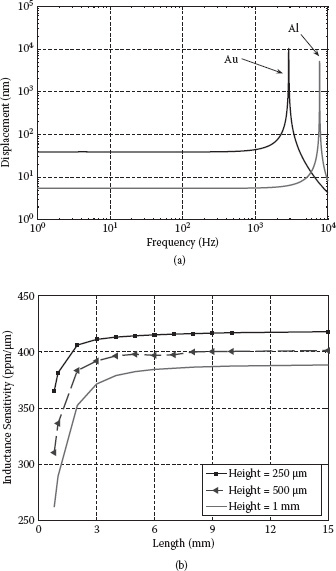
FIGURE 13.3 FEM simulated (a) frequency response of Au and Al bondwires; (b) inductance sensitivity versus length.
13.2.6 RESOLUTION AND NOISE FLOOR
There are two major noise sources in an accelerometer: (1) mechanical noise and (2) electronic interface noise. Brownian motion creates the mechanical noise of a structure, which is a type of mechanical-thermal noise caused by molecular collisions from the surrounding environment. The noise source represents the fundamental noise limit of an inertial sensor. The Brownian noise equivalent acceleration (BNEA) can be calculated using [14]
(13.7) |
where KB is Boltzmann constant, T is the absolute temperature, D is damping constant, Ma is proof mass, and QMech is the mechanical quality factor. To reduce the mechanical noise in an accelerometer system, a large proof mass, a high mechanical quality factor, and a low mechanical resonant frequency are needed. For instance, a 3.5 mm length and 25 μm diameter gold bondwire has a mass of 30 μg, a resonant frequency of 3 kHz, and a QMech of 200, which leads to a BNEA noise density of 0.73μg/√(Hz) at room temperature. Since this noise density is so small, electrical interface noise usually dominates the resolution of the acceleration sensor system. Therefore, minimizing electronic noise is critical. An analysis of electrical interface noise will be presented in Section 13.3.
Bondwires can appear as explicit or parasitic inductors. They have a larger surface area per unit length compared to planar spiral inductors and are further from the ground plane. This increased distance from the ground plane reduces parasitic capacitance and substrate losses, resulting in a high Q inductor. The electrical properties of bondwires depend on their physical dimensions: the height above the die plane, the horizontal length, and the distance between other adjacent bondwires. When we ignore the nearby conductor effects, the self-inductance of a bondwire is [15]
(13.8) |
The mutual inductance of two parallel bondwires with equal length is approximately
(13.9) |
where d is the distance between them. For a pair of bondwires carrying a differential current, the total inductance is
(13.10) |
The inductance sensitivity to displacement is defined by
(13.11) |
and is plotted in Figure 13.3(b). Both the total inductance and mutual inductance increase with the length of bondwire; however, when the length becomes excessively large
(13.12) |
the inductance sensitivity becomes independent of the length. Thus, there is an optimal choice for length of the bondwire sensor, which will maximize sensitivity and minimize the sensor size.
Note that this calculation is used to illustrate an idea and models a pair of parallel bondwires that undergo the same fixed relative displacement across their entire length. In practice, the peak displacement only occurs at the apex of the bondwire since the two ends are fixed. Thus, the FEM simulation results of two parabolic bondwires with fixed ends shows a much smaller inductance sensitivity (Figure 13.3b) than what is predicted from calculation. The bondwire spacing is set by the bondpad pitch used in the CMOS fabrication process, so it is typically not a design parameter. In our process (0.13 μm), the on-chip bond pad spacing is about 90 μm, which results in a 390 ppm/μm inductance sensitivity (FEM simulation) for a 3 mm length bondwire.
13.2.8 TEMPERATURE AND FABRICATION VARIATION
Bondwire inductance varies with temperature and package assembly (due to the bonding strength and machine tolerances). The temperature coefficient (TC) of a bondwire inductor comes from (1) the linear expansion of the wire with increasing temperature and (2) the change in the contribution of the internal flux to the total inductance [15]. The internal flux is inversely proportional to frequency due to the skin effect reducing the effective conductor area. Usually, the total inductance of a bondwire inductor has a TC of roughly 50–70 ppm/°C at 1 GHz. In addition, the TCs for the resistivity of gold and aluminum are 3400 ppm/°C and 3900 ppm/°C, respectively.
In addition to temperature variations, the bonding process can affect bondwire inductance since a bondwire’s inductance depends on its structure and geometry. To enhance the precision of bonding and eliminate board/package stress, the sensing gold and aluminum wires can be bonded between pads on the same chip (instead of chip to package), which more precisely controls the length and separation of the bondwires. Chip-to-chip wire bonding can reduce inductance deviation to ~6% [16], which is comparable to the variation of on-chip inductors and capacitors in a standard IC technology design (>10%). This value is tolerable in standard IC design since on-chip capacitors and inductors typically have a variation larger than 10%.
13.3 ELECTRICAL READOUT INTERFACE FOR BONDWIRE ACCELEROMETER
13.3.1 SYSTEM ARCHITECTURE FOR BONDWIRE INERTIAL SENSING
Figure 13.4 shows the diagram of the proposed sensing scheme using a bondwire inertial sensor. A dense and relatively elastic gold (Au) wire is used in conjunction with a stiff and less dense aluminum (Al) wire to create an inertial sensor. The difference in material properties creates a relative deflection between the two bondwires during acceleration. Despite the fact that Au and Al have a similar Young’s modulus, Au is 7.14 times denser than Al, resulting in a much greater bondwire displacement for the same applied acceleration. The relative displacement of adjacent bondwires changes their mutual inductance, which is then converted to a frequency deviation using an oscillator. Due to the small displacements of the bondwire and the corresponding small changes in inductance under acceleration, the oscillator frequency can be linearly approximated as
(13.13) |
where C is an on-chip capacitance that is independent of acceleration. For example, for a 2 GHz bondwire oscillator with an inductance sensitivity of 350 ppm/μm and a 30 nm relative displacement due to a 1 g acceleration, the center frequency will shift by 10.5 kHz, which is detectable by an on-chip demodulator. In addition, the oscillator has a large amplitude output (hundreds of millivolts), which is less sensitive to induced noise in the following stages. Further, the frequency modulated signal also offers immunity to amplitude noise.
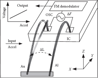
FIGURE 13.4 System diagram of the proposed bondwire inertial sensor.
13.3.2 ELECTRICAL NOISE IN READOUT CIRCUITRY
In a frequency modulated (FM) system, frequency uncertainty can be described by phase noise, Allan variance, and residual frequency noise. Phase noise represents the short-term frequency stability, whereas the Allan variance signifies the long-term frequency stability in the time domain. Residual frequency noise represents the RMS frequency fluctuation, which can be derived from the phase noise measurement.
In an LC oscillator design, losses in the resonant tank, periodic variations of the active device parameters, and nonlinearity of devices can all contribute the amplitude and phase fluctuations. To simplify the analysis, the phase noise of an oscillator can be approximately modeled by Leeson’s phase noise formula [17]:
(13.14) |
where F is the oscillator noise factor, Q is the quality factor of the resonant tank, T is the absolute temperature, and Prf is the average power at the output of the oscillator. Phase noise improves linearly as carrier power increases and quadratically as increases. Bondwire inductors typically have a Q factor of 30–70 at frequencies in the low gigahertz, resulting in excellent oscillator noise performance.
Biomedical signals usually require a low sampling rate; therefore, long-term frequency stability is also important to sensor performance. The time domain frequency stability measurement is based on the statistical analysis of the phase/frequency fluctuation as a function of time. The Allan variance can be described as
(13.15) |
where is the nth average over the observation time τ. Figure 13.5 shows an example Allan variance plot and is displayed in a log-log scale. Five basic phase and frequency noise sources contribute noise in three regions of the Allan variance plot. The regions define acceleration sensor noise performance in terms of resolution, bias stability, and drifts from environmental effects, such as temperature and aging. Frequency/phase domain and time domain conversions can be expressed between the slopes of phase noise and Allan variance [18,19]. With respect to sensor design, the Allan variance plot shows the optimized integral sampling time for achieving minimum resolutions by minimizing the flicker frequency noise.

FIGURE 13.5 Allan variance plot.
Residual frequency is an important specification that defines the RMS value of the frequency fluctuation within a frequency range. It can be derived from the phase noise of an oscillator as
(13.16) |
where £(fm) is the single sideband (SSB) noise power spectral density, and fm is the offset from the carrier frequency. The integration in (13.16) can be performed using a known phase noise profile within the sensor bandwidth. Assuming the gain of the accelerometer is 10 kHz/g and a phase noise slope of –20 dB/decade, calculations show that the oscillator requires a phase noise of approximately –50 dBc/Hz at 10 kHz offset frequency to achieve a full bandwidth (5 kHz) resolution of 0.1 g. Increasing the power consumption of the oscillator, using a higher Q resonant tank, or limiting the bandwidth of the sensor signal can further improve the resolution.
Figure 13.6 shows the overall circuit block diagram of the implemented inertial sensor readout system. The sensor readout circuit consists of a 2 GHz sensing oscillator (VCO1), a phase locked loop (PLL), mixers, baseband amplifier, a bandgap temperature-stabilized bias circuitry, and a low dropout (LDO) supply regulator. One major difference between the sensor readout architecture and a traditional FM radio receiver is the input signal strength. Our sensor architecture needs to handle a fixed large signal input, where an FM radio requires wide dynamic range and the signal is usually small. The large input signal amplitude makes the sensor architecture less susceptible to noise from the down-conversion stages. In addition, using an FM detection architecture provides more relaxed requirements for the linearity of the mixer and IF amplifiers. However, one of the major design concerns with this architecture is signal locking between oscillators. To eliminate this effect, the parasitics in the signal path and substrate coupling must be minimized and the two oscillator frequencies must be sufficiently different. Therefore, the frequency-modulated signal (2 GHz ± 10 kHz) was set 20 MHz away from the stable reference frequency from PLL. Once the signals are down-converted (20 MHz ± 10 kHz), they can be easily detected and digitalized for further signal processing.

FIGURE 13.6 System blocks of readout circuitry.
A cross-coupled differential oscillator is chosen to suppress common-mode noise. To reduce noise up-conversion due to nonlinearity, varactors were avoided. In order to compensate for variations in the wirebonding process and fabrication, the oscillator is tunable from 1.5 to 2.5 GHz by utilizing a 4-bit discrete capacitor bank. To further enhance the power supply rejection ratio (PSRR) and reduce the temperature dependency of the sensing oscillator’s frequency, an on-chip bandgap reference and low dropout regulator (LDO) are used to convert a 1.5 V external battery supply to an on-chip 1.2 V supply. The regulator can accommodate a load current up to 16 mA with only a 10 mV drop from the desired 1.2 V output. The maximum voltage deviation is 7 mV across temperature, and the measured low frequency PSRR is 32 dB from 1.35 to 1.55 V.
The clock signal is generated by a third-order type II PLL. The PLL oscillator design is similar to the bondwire sensing oscillator design. A MOS varactor was added to tune oscillator frequency continuously (by about 100 MHz/V) within the sensor frequency band (1.5–2.5 GHz), which is set by a 4-bit capacitor bank. The in-band noise induced by the nonlinearity of the varactor is suppressed by the loop when the oscillator is locked to the crystal frequency reference. Thus, the noise of the entire system is dominated by the free-running sensing oscillator (VCO1). The phase-frequency detector was designed using true single-phase clock logic (TSPC), which has higher speed than static logic and provides less in-band phase noise. A differential charge pump circuit is employed to reduce the common mode noise and minimize the effects of charge injection and signal feed-through. All schematic components are fully integrated except the crystal resonator. It should be noted that, since an accurate time reference is not critical, even the crystal resonator can be eliminated if necessary.
The RF mixer down-converts the modulated RF signal to a low frequency to facilitate demodulation. Unlike conventional FM receivers, the mixer in this design is driven by two large signals. Though this provides noise immunity, it also leads to signal distortion and LO pulling that can overwhelm the input signal. CMOS passive mixers have been demonstrated to produce better linearity and low flicker noise [20]. A two-stage cascaded buffer inserted between the oscillator and the mixer reduces the effect of LO pulling in the sensing oscillator. The third-order active RC low pass filter amplifies the signals and consequently reduces the effect of amplitude-induced errors in the baseband demodulator. The detailed circuit analysis and measurement results can be found in Liao, Biederman, and Otis [12].
13.5 EXPERIMENTAL RESULTS OF THE SINGLE AXIS BONDWIRE ACCELEROMETER
The bondwire accelerometer, fabricated in a 0.13 μm CMOS process, is completely integrated in a 1 × 1.1 mm2 area, except for an 8 MHz quartz crystal reference and bypass capacitors. Figure 13.7 shows the assembled PCB and micrograph of the prototype accelerometer. To reduce the PCB strain or other undesired external forces, the accelerometer chip was mounted in a 44-pin plastic leaded chip carrier (PLCC) package using aluminum/gold wedge wire bonding without encapsulation and was powered by one AA battery on the PCB. Two commercial accelerometers for three-axis and large acceleration measurement were mounted on the PCB near the chip to ensure accurate calibration of the applied acceleration from a shaker table. The prototype PCB was mounted on a custom machined aluminum platform to maximize the mechanical energy transferred from the shaker table to the accelerometers. An oscilloscope and a spectrum analyzer were used to monitor the accelerometer outputs.
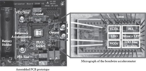
FIGURE 13.7 Assembled PCB prototype and micrograph of the accelerometer IC. The active area is outlined in white boxes.
Using the shaker table, an acceleration of 1g at 40 Hz was applied along the sensitive axis (X) of the bondwire accelerometer. The output was compared to the commercial accelerometers after normalizing for differences in gain. The comparison result is presented in Figure 13.8(a) and shows that the bondwire accelerometer is capable of real time acceleration tracking. Figure 13.8(b) shows the measured accelerometer frequency response, exhibiting a gain of 10 kHz/g within a 700 Hz bandwidth. The mechanical resonances of the Au and Al bondwires are visible at approximately 3.1 and 8.7 kHz, respectively, which is consistent with the FEM simulation. Figure 13.8(c) shows the measurement results of a three-axis acceleration test on the bondwire accelerometer, revealing a linear gain of 10 kHz/g (matching calculations) and greater than 20 dB isolation between the sensitive axis (X) and nonsensitive axes (Y and Z).
As a control, the same test was performed on a chip that was completely encapsulated in nonconductive epoxy (Stycast 1266). The goal of this experiment was to show decisively that the frequency deviations under acceleration were caused by bondwire deflection. The control package exhibited no detectable output from acceleration along any axis. Finally, a 90° rotation test with acceleration only from gravity was performed on non-encapsulated sensor, and the result is plotted alongside the expected sinusoidal response in Figure 13.8(d).
Figure 13.9(a) shows the measured phase noise of the sensing oscillator, PLL, and IF stage, confirming that the accelerometer noise floor is dominated by the free-running sensor oscillator. The bondwires exhibit a high electrical quality factor (Q ~ 40), allowing a low sensor oscillator phase noise of –64 and –121 dBc/Hz at 10 kHz and 1 MHz offsets, respectively, while consuming 2 mA.
The Allan variance is often used to define a clock system and resonant sensor performance [19]. Figure 13.9(b) shows the measured Allan variance of the outputs of the sensing oscillator, PLL, and IF with a sample rate of 1 Hz. The Allan variance gradually flattens out as average time increases. The drift is most likely caused by the temperature and environment fluctuations, which can be removed with feedback control to VCO1. Furthermore, this plot reveals that the accelerometer has a resolution of 80 mg and a bias stability of 35 mg for a 10 s integration window. The noise floor of this accelerometer is limited by the phase noise of the sensing oscillator, not by mechanical noise sources. Accelerometer performance is summarized in Table 13.3.

FIGURE 13.8 Measured results of the bondwire accelerometer: (a) waveforms; (b) frequency response (c) a three-axis acceleration test; (d) the rotation test.
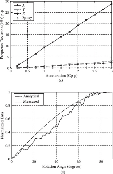

FIGURE 13.9 Measured (a) phase noise and (b) Allan variance at the output of the sensing oscillator, PLL, and IF stages.
Technology |
0.13 µm CMOS |
Chip area |
1 × 1.1 mm2 |
Sensing oscillator frequency |
2.1 GHz |
PN at 10 kHz |
-64 dBc/Hz |
PN at 1 MHz |
-121 dBc/Hz |
Sensitivity |
10 kHz/g |
Bandwidth |
700 Hz |
Axis isolation |
>20 dB |
Resolution |
80 mg |
Bias stability |
35 mg |
Power consumption |
13.5 mW |
13.6 CONCLUSIONS AND DISCUSSION
Successful deployment of wireless sensors to provide ambient intelligence for healthcare will require a confluence of progress in materials, sensor integration, low power electronics, RF communication, and packaging. CMOS-based sensor systems are promising for many healthcare and biomedical applications due to their robustness and low cost. By combining advanced microelectronics and sensors on a single chip, the system offers unique opportunities to perform high-resolution measurements in a variety of applications. In this chapter, we focused on the design and implementation of the first inertial sensor to use bondwires, which can be readily integrated into any IC process. Bondwires can be incorporated onto chips with existing fabrication techniques without complicated MEMS processes and can potentially be mass manufactured at low cost.
The principle of operation, as well as the mechanical and electrical properties of bondwire accelerometers, were explained in detail in Section 13.2. By exploiting advanced IC technology, a bondwire accelerometer has potential to integrate a wireless transmitter and digital processing, all on a single chip. A single-chip bondwire accelerometer has demonstrated performance suitable for many applications, such as fall detection, body movement monitoring, and orientation display. In the future, further data processing/functions can be added into a square millimeter-sized silicon chip (e.g., real-time functionality configuration and calibration such as bandwidth, resolution, and acceleration sensitivity). With further advances in bondwire design, coating isolation, and packaging, the system could perform many measurement functions, such as mechanical, inertial, or magnetic sensing, at a low fabrication complexity and cost.
1. A. Lombardi, M. Ferri, G. Rescio, M. Grassi, and P. Malcovati, Wearable wireless accelerometer with embedded fall-detection logic for multi-sensor ambient assisted living applications, in IEEE Sensors Conference Proceedings, pp. 1967–1970 Oct. 2009.
2. C.-F. Lai, S.-Y. Chang, H.-C. Chao, and Y.-M. Huang, Detection of cognitive injured body region using multiple triaxial accelerometers for elderly falling, IEEE Sensors Journal, vol. 11, no. 3, pp. 763–770, March 2011.
3. S. Patel, K. Lorincz, R. Hughes, N. Huggins, J. Growdon, D. Standaert, M. Akay, J. Dy, M. Welsh, and P. Bonato, Monitoring motor fluctuations in patients with Parkinson’s disease using wearable sensors, IEEE Transactions on Information Technology in Biomedicine, vol. 13, no. 6, pp. 864–873, Nov. 2009.
4. C. Bouten, K. Koekkoek, M. Verduin, R. Kodde, and J. Janssen, A triaxial accelerometer and portable data processing unit for the assessment of daily physical activity, IEEE Transactions on Biomedical Engineering, vol. 44, no. 3, pp. 136–147, March 1997.
5. D. Crescini, D. Marioli, and A. Taroni, Low-cost accelerometers: Two examples in thick-film technology, Sensors and Actuators A: Physical, vol. 55, no. 2–3, pp. 79–85, 1996.
6. C. Verplaetse, Inertial proprioceptive devices: Self-motion-sensing toys and tools, IBM Systems Journal, vol. 35, no. 3.4, pp. 639–650, 1996.
7. R. N. Stiles, Frequency and displacement amplitude relations for normal hand tremor, Journal Applied Physiology, vol. 1, no. 40, pp. 44–54, Jan. 1976.
8. Y. Wang, J. Fan, P. Xu, J. Zu, and Z. Zhang, Shock calibration of the high-g triaxial accelerometer, IEEE Instrumentation and Measurement Technology Conference Proceedings, pp. 741–745, May 2008.
9. R. Olsson, K. Wojciechowski, M. Baker, M. Tuck, and J. Fleming, Post-CMOS-compatible aluminum nitride resonant MEMS accelerometers, Journal of Microelectromechanical Systems, vol. 18, no. 3, pp. 671–678, June 2009.
10. L. He, Y. P. Xu, and M. Palaniapan, A CMOS readout circuit for SOI resonant accelerometer with 4 μg bias stability and 20-μg / Hz H resolution, IEEE Journal of Solid-State Circuits, vol. 43, no. 6, pp. 1480–1490, June 2008.
11. J. Wu, G. Fedder, and L. Carley, A low-noise low-offset capacitive sensing amplifier for a 50 μg/√Hz monolithic CMOS MEMS accelerometer, IEEE Journal of Solid-State Circuits, vol. 39, no. 5, pp. 722–730, May 2004.
12. Y.-T. Liao, W. Biederman, and B. Otis, A fully integrated CMOS accelerometer using bondwire inertial sensing, IEEE Sensors Journal, vol. 11, no. 1, pp. 114–122, Jan. 2011.
13. H. A. Schafft, Testing and fabrication of wire-bond electrical connections: A comprehensive survey, US National Bureau of Standards, 1973.
14. B. Boser and R. Howe, Surface micromachined accelerometers, IEEE Journal of Solid-State Circuits, vol. 31, no. 3, pp. 366–375, March 1996.
15. T. H. Lee, The design of CMOS radio-frequency integrated circuits, Cambridge University Press, 2004.
16. J. Craninckx and M. Steyaert, A 1.8 GHz CMOS low-phase-noise voltage-controlled oscillator with prescaler, IEEE Journal of Solid-State Circuits, vol. 30, no. 12, pp. 1474–1482, Dec. 1995.
17. D. Leeson, A simple model of feedback oscillator noise spectrum, Proceedings of the IEEE, vol. 54, no. 2, pp. 329–330, Feb. 1966.
18. O. Baran and M. Kasal, Allan variances calculation and simulation, Radioelektronika, 19th International Conference, pp. 187–190, 2009.
19. N. El-Sheimy, H. Hou, and X. Niu, Analysis and modeling of inertial sensors using Allan variance, IEEE Transactions on Instrumentation and Measurement, vol. 57, no. 1, pp. 140–149, Jan. 2008.
20. S. Zhou and M.-C. Chang, A CMOS passive mixer with low flicker noise for low-power direct-conversion receiver, IEEE Journal of Solid-State Circuits, vol. 40, no. 5, pp. 1084–1093, May 2005.