4
Telecommunications Economies of Scale
4.1 Market Size and Projections
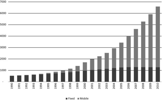
The starting point of this chapter is the remarkable rise of mobile connectivity relative to fixed connectivity as a percentage of the world market expressed in terms of global connections.
Figure 4.1 is sourced from our colleagues at The Mobile World, as are all the market and business statistics used in this book, and shows a crossover point in 2002 when mobile matched fixed for the first time and then a year-on-year transition to where we are today with an almost five-to-one relationship.
Figure 4.1 Global connections, 1990 to 2010. Reproduced with permission of The Mobile World.
This of course has had a profound and largely positive impact on the part of the industry supply chain that services the mobile market, though we argued in our introduction that overspending on spectral investment has constrained R and D spending in some critical areas including some areas of RF component innovation that in turn has made it more difficult to get a return from that investment.
Table 4.1 provides a simplified overview of this supply chain.
Table 4.1 Industry supply chain
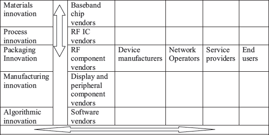
The arrows denote risk and value distribution that can either be horizontal or vertical. Risk is a poison chalice that tends to get moved around. Sometimes some parts of the supply chain take the risk and others realise the value. The risk–reward equation, as we shall see, is influenced significantly by market volume. Figure 4.2 shows actual sales to 2010 and forecast sales through to 2013.
Specifically in this chapter and the next we set out to track the supply-chain changes that have occurred between 2007 and 2012, a period in which sales will have grown from 1.1 billion units per year to 1.7 billion units per year and project that forward to take a view on how the supply chain will look in the future.
All those unit sales suggest a lot of people have mobile phones and that a lot of people have multiple mobile phones which explains why many countries, Finland being one example, have penetration rates significantly higher than 100%.
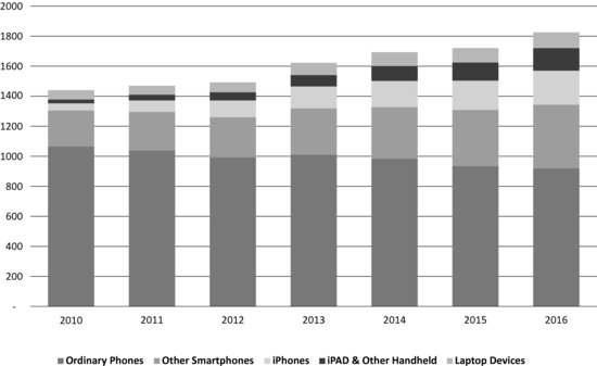
Figures 4.3 and 4.4 below also show the mix of devices split as ordinary phones, iPhones and other smart phones, iPAD and similar tablet form factor devices and lap top devices. The iPhone launched in 2007 still has a relatively small global market share but spawned a new product sector of enhanced functionality smart phones. This has had a major impact on service revenues and service and delivery costs. The launch of the iPad in 2010 appears to be creating another new sector that will likely have a similarly transformative impact that should be positive, provided delivery and support cost can be rigorously controlled. A topic to which we return on several occasions.
Figure 4.2 Mobile device sales, 2003–2016. Reproduced with permission of The Mobile World.
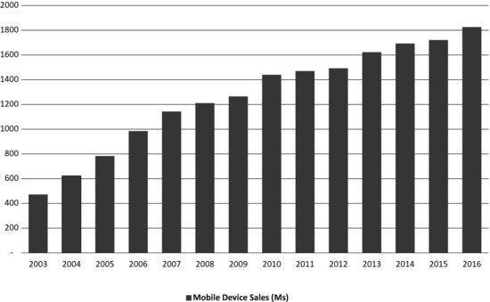
Figure 4.3 Global mobile device population 2010 to 2016. Reproduced with permission of The Mobile World.
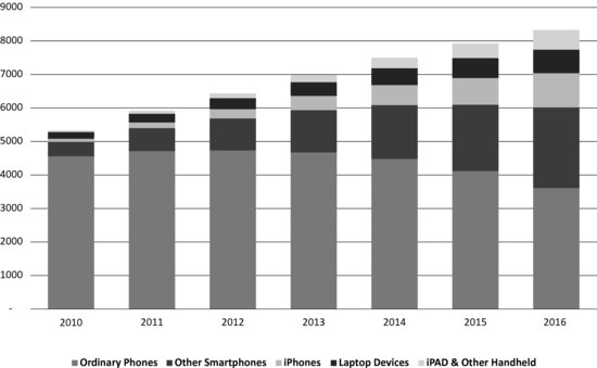
The trend clearly shows ordinary phones becoming a smaller part of the mix. Given that much of the volume growth is from developing economies with low GDP relative to developed economies this might seem surprising. It probably shouldn’t be. People in fast-growing economies are willing to spend a larger percentage of their monthly income on mobile connectivity both for practical reasons and as a demonstrable token of ambition and/or success. Some developing countries also have high multiple-occupancy ratios, the number of people living in one household, which means that the disposable income available for this type of discretionary spending is higher than might be expected.
Figure 4.4 Mobile device sales by type 2010 to 2016. Reproduced with permission of The Mobile World.
This shift in product mix is also having a significant impact on offered traffic. An ordinary phone supporting predominantly voice and text will typically generate an average of 30 megabytes or so of offered traffic per month. A smart phone will generate between 300 and 500 megabytes and a lap top with mobile broadband connectivity about 2 gigabytes. The result in many markets is that data volumes are presently quadrupling on an annual basis. Most forecasts, including our own, have been underestimating the rate of growth and present forecasts may also prove overconservative.
Figures 4.5 and 4.6 takes the unit volumes and offered traffic data points and calculates the offered traffic on a per device basis. Note that data volume does not necessarily translate into data value particularly in markets where ‘all you can eat’ tariffs are supported. This is because a high data user can inflict significant collateral damage to other users in the cell. This in turn creates an opportunity cost that in a percentage of cases will be higher than the income generated from the device. Traditionally users/subscribers have been analysed by network operators in terms of average revenues per user (ARPU) but increasingly now should be measured either in terms of AMPU (average margin per user) or more accurately AMPD (average margin per device).
Figure 4.5 Mobile data volume per month (Exabytes) 2010 to 2016. Reproduced with permission of The Mobile World.
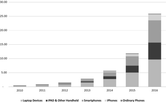
Figure 4.6 Annual mobile data traffic (Exabytes) 2010 to 2016. Reproduced with permission of The Mobile World.
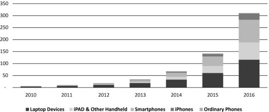
The scale shift is, however, quite remarkable. An exabyte by the way is a million terabytes.
The impact on the relative revenue mix between voice and data is shown in Figure 4.7 with projections forward to 2016.
Figure 4.7 Mobile service revenue – 2010 to 2016. Reproduced with permission of The Mobile World.
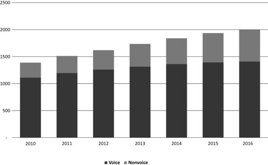
However, revenue is not the same as profitability. If a network is lightly loaded, incremental loading, as long as it has some revenue attached to it, will improve network investment return rates. If the network is heavily loaded and additional load requires additional capacity to be added, then return on investment is dependent on the investment per subscriber per megabyte. This is not a metric that operators have previously needed to be concerned about.
Adding capacity may also imply an investment in new spectrum. The economics of this are complex as a return on investment is dependent on ensuring an adequate supply of performance competitive market competitive user devices are available. For reasons that we will analyse this is often much harder to achieve than one might expect and is a function of RF cost economics. RF cost economics are a function of the band plan but also the technology deployed in each supported band.
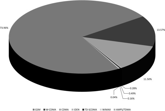
Figure 4.8 shows the absolute dominance of GSM on a global basis. This is effectively a technopoly – a market dominated by a legacy technology. This has advantages and disadvantages. If you don’t happen to have GSM deployed in your network it is definitely a disadvantage as you will be exposed to an alternative technology that is subscale.
A design and manufacturing team will typically get a better return from servicing a large established mainstream market and certainly would be wary of the opportunity cost implicit in diverting resources away from what should be a dominant income stream.
But also there is a question as to how fast newer technologies are adopted. The adoption rate is driven by the scale difference in user experience between the old and new technology and the relative cost of delivery. To date neither the scale difference between 3 G and 2 G systems or the relative delivery economics or the user experience difference have been sufficient to drive a radically fast transition. As Figure 4.8 shows even taking WCDMA and CDMA together they still only represent 25% of the market ten years after market introduction.
Figure 4.8 Mobile connections by technology Q1 2011. Reproduced with permission of The Mobile World.
We also need to take into account relative shifts in terms of regional importance and how these might affect future value ownership in the industry. In our introduction we highlighted the rapid rise of China and Asia Pacific in general as the globally dominant market for telecommunication products and increasingly as a manufacturing and development centre of telecommunication products, both for its internal market and rest of the world markets.
Figure 4.9 tracks this trend over the five years from 2005 to Q1 2011 and shows the relative decline of the US as a market measured in terms of mobile connections – a remarkable change considering that 15 years earlier the US represented 70% of the global market by volume and value.
Figure 4.9 Mobile connections by region 2005 to Q1 2011. Reproduced with permission of The Mobile World.
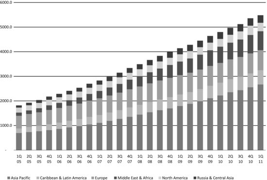
Figure 4.10 Leading mobile operators controlled connections, Q1 2011. Reproduced with permission of The Mobile World.
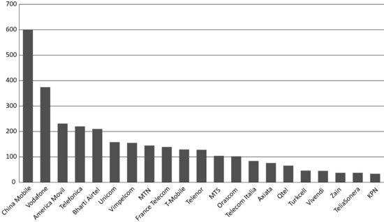
Figure 4.11 Leading multinational mobile operators proportionate connections, Q1 2011. Reproduced with permission of The Mobile World.
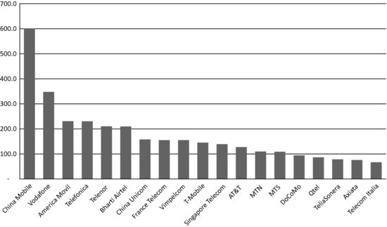
Figure 4.12 Mobile connections, China 2001 to 2010. Reproduced with permission of The Mobile World.
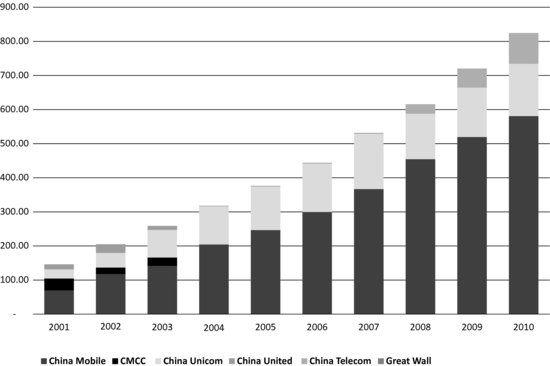
Figure 4.10 shows the relative market presence of the top twenty operators with China Mobile as the dominant player.
Figure 4.11 proportionate connections taking into account crossownership where operators have shareholdings in other operators.
Figure 4.12 shows China Mobile’s dominance relative to other carriers in the China market. China Mobile acquired China Telecom’s mobile businesses in four phases. China Unicom was formed by the merger of China United and Great Wall. China Telecom re-entered the mobile business in 2008 by acquiring Unicom’s CDMA business. All three use different 3G technologies, a triumph of politics over technical common sense.
4.2 Market Dynamics
In this chapter we study the impact of these market dynamics on the supply chain, how economies of scale determine the allocation of R and D resource, related gravitational investment effects, the influence of standards making on this process, the influence of the spectral auction and allocation process, the role of enabling technologies at component level and the role of component technologies at system level.
We find that even in China and even for China Mobile, the economics of deploying a mobile broadband network into nonstandard spectrum are substantially subscale. It might be expected that China Mobile’s apparent market leverage could be translated into aggressive component price reduction and aggressive innovation. Actually, this proves not to be the case. Attempting to also deploy nonstandard technologies into these bands introduces additional risks and costs. The associated costs are incurred partly on the network side (base station costs) but predominantly get reflected in handset and user equipment costs both in terms of direct component cost, design risk, time to market risk and performance risk, all of which have additional cost and revenue-loss implications.
An analysis of this can be found in the RTT Study RF Cost Economics for Handsets undertaken for the GSM Association in September 2007 and available as a free download,1 but the following is a synopsis to avoid you having to read a 92 page document.
The opening assumption is that there is an underlying and ongoing need to lower user device costs and provide a continuously improving user experience in terms of data rates and duty cycles and a parallel need to support multiple simultaneous data streams. The ongoing need for lower user device costs is debatable but let’s go with it for the time being.
Cost reduction in all consumer electronics products is typically achieved by realising higher levels of integration. However, RF functions have been traditionally difficult to integrate. For example, the higher power levels used in wide-area cellular systems make it problematic to place devices such as RF power amplifiers in close proximity to other RF and non-RF functions. RF devices do not scale in the same way as other devices and obey Ohms law rather than Moore’s law.
In terms of spectral policy making, it is assumed that future cellular phones will become increasingly frequency transparent, able to access multiple frequencies across multiple bands. However, this requirement is at odds with the parallel need to increase integration levels to achieve ever lower component and production cost targets. A more highly integrated phone does not necessarily make it easier to add new bands for example, and it can be easier to add bands with more discrete solutions. It is certainly easier and cheaper to fix mistakes in less highly integrated designs.
As integration levels increase, the number of RF components reduces, the RF bill of materials (RF BOM) goes down and production costs go down. However, moving to a higher level of integration implies an increase in nonrecurring engineering costs. The cost of design mistakes becomes higher.
An increase in nonrecurring RF engineering and design costs also implies that higher market volumes are needed to achieve RF economies of scale. NRE costs can be reduced by adopting lower levels of device integration but the RF BOM will increase and the form factor of the phone will increase. RF performance may or may not decrease but will be more variable from phone to phone (handset to handset, batch to batch variations from the production line).
Although handsets are becoming more integrated over time, the practical implementation of a single-chip software-definable phone remains elusive. It is relatively easy to count at least 100 separate components in a phone, including modules that themselves contain multiple functions on separate parts of a common substrate. About 75% of these components in present cellular phones are passive, inductors, capacitors and filters. These devices are frequency specific.
Supporting additional frequencies in a handset implies an increase in the number of passive components. This implies higher material and manufacturing costs. Active devices such as the power amplifier can be designed to cover relatively wide frequency bands but become harder to match and lose overall efficiency. Nonstandard frequency allocations therefore have an impact on passive and active device requirements.
New MEMS (microelectrical mechanical system) -based technologies offer the potential opportunity to integrate many of these functions onto an RFIC, including for example, switch and tuneable filter functions. Tuneable structures integrated with other active components can be used to implement wideband power amplifiers, broadband tuneable matching networks and adaptive antenna matching.
Similarly, MEMS devices may be used to vary the load impedance of power amplifiers so that they will work efficiently at varying power levels over a relatively wide range of frequencies. MEMS also potentially address the problem of duplexing, particularly in 3G phones. In GSM, duplexing, (the separation of transmit and receive channels within a specific frequency band) can be achieved with a front-end switch as the phones are not transmitting and receiving at the same time.
In WCDMA, HSPA and LTE, transmission takes place at the same time as reception. Adding a band means another duplex filter needs to be added that has an associated direct cost and an associated indirect cost (takes up additional board space and needs matching components).
There are presently proposals for MEMS-based active digitally tuneable duplexers, also known as digital duplexers, which may potentially resolve these band-specific 3G specific duplex cost overheads. These techniques together will enable a transition towards single-chip software-defined radios that will help eliminate many present spectrally specific device and design issues.
Five years ago when this study was written these devices were claimed to be ready for market. However, five years later their application in terms of functional replacement of traditional RF components is limited for reasons that we explore in Chapter 5.
This highlights a pervasive disconnect in our industry. Spectral allocation and auction policy and technology policy, or rather the absence of technology policy known as ‘technology neutrality’ is generally based on an assumption that technology is actually capable of solving all problems within defined time scales. There are several problems with this problem. Some performance metrics are defined by the basic rules of physics and cannot be resolved by material, component level or algorithmic innovation. Additionally, problems that can be resolved by innovation take longer to resolve than expected. In wireless we find that RF component innovation in particular moves slowly and introduces additional unexpected costs throughout the supply chain, especially for the operator and service provider community. Also, sufficient incentives need to be in place to ensure adequate innovation occurs at the right time and sufficient engineering effort is applied to translate that innovation into practical fiscal gain. This sets the narrative for both the remainder of this chapter and Chapter 5.
Figure 4.13 shows the main functional components in a modern multimedia handset. The ‘front-end’ filters and diplexers deliver a signal path to and from the baseband signal processor. On the receive path, a power-detection function measures the received signal strength that determines the amount of transmit power being used on the transmit path. The transmit path includes the power amplifier. The baseband signal processor filters the received signal and provides an interface to all other devices in the phone including the display, audio paths, voice paths and camera module. This example also includes a MEMS motion sensor.
Figure 4.13 Functional block diagram of a modern multimedia handset. Reproduced with permission of MediaTek (previously Analog Devices).
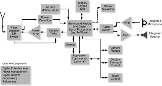
From the above, it might be assumed that the cost of the RF functions in the phone are reducing as an overall percentage of the total costs as additional non-RF functions are added.
However, the RF bill of materials has stayed more or less constant as a percentage of the overall bill of materials This is due to the addition of additional frequency bands and additional functionality, for instance in the above example, the addition of a mobile TV receiver.
Actually, as most of us will have noticed very few phones ever ended up with mobile TV receive functionality, for reasons we explore in Chapter 15. However, additional bands have been added that have introduced at least equivalent amounts of complexity. Additionally, the broadcast community is promoting the development and deployment of ATSC and DVB T services to portable devices in spectrum that is immediately adjacent to the US 700-MHz and European 800-MHz mobile broadband spectrum. This is unsurprising as these bands have been created from the switchover from analogue to digital TV.
One issue therefore is to consider the behaviour of user equipment front ends when handling a broadcast receive path and mobile broadband transceiver functionality. The broadcast receive path is relatively wideband and therefore vulnerable to interference from any transmit energy produced in the user’s device or by other proximate users. The characterisation of this transmit energy is in turn a function of the band plan and spectral masks deployed in the mobile broadband user device.
4.3 Impact of Band Allocation on Scale Economics
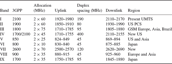
In 2007 there were nine RF duplex spaced cellular frequency bands between 800 MHz and 2.6 GHz specified by 3GPP (the 3G Partnership Project) either presently used by GSM or UMTS and/or are considered suitable for longer-term UMTS implementation.
The nine bands are shown in Table 4.2.
Table 4.2 Band allocations and duplex spacing
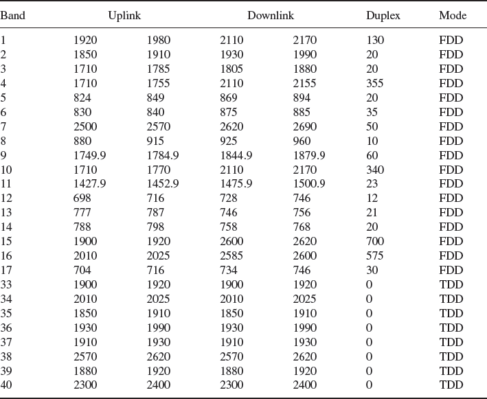
Five years later in 2012 this had expanded to 25 bands including eight additional TDD bands. These are shown in Table 4.3.
Table 4.3 Twenty-five band allocations
Release 9 of the 3GPP specifications define four further bands, three being extensions or variations of the 850 MHz band and the other being around 1500 MHz. Bands 18 and 19 extend the existing 850 band adding 10 MHz at the lower end of the present Band V allocation to provide a 35-MHz rather than a 25-MHz pass band. Band performance relative to Band V would be degraded by about 1 dB.
The bands made available by the digital switch over at 700 MHz in the USA and 800 MHz in Europe have also introduced particular challenges, which we review in Chapter 5.
On the 28 June 2010, the US Obama administration issued a memorandum stating an intention to auction a further 500 MHz of spectrum over and above present allocations. Some but not all of this will line up with rest of the world band plans and may or may not include spectrum in L band at 1.4, 1.5 and 1.6 GHz and S band allocations presently ring fenced for hybrid satellite/terrestrial networks.
Additionally in some form factors, for example tablets, slates and lap tops, there may be a future need to integrate ATSC TV receive and/or DVB T2 receiver functionality in the 700-MHz band for portable rather than mobile reception. This receive capability has to coexist with locally generated frequency duplexed (FDD) and time-domain duplexed (TDD) transmit energy.
4.3.1 FDD versus TDD
At this point a short digression into the relative merits of FDD and TDD is needed.
A traditional FDD duplex band plan is shown in Table 4.4. The duplex gap in a cellular/mobile broadband handset keeps the TX power from one set of users getting in to the receive band of another set of users. The duplex spacing keeps locally generated transmit power out of the receive path in the user’s device.
Table 4.4 Traditional FDD duplex band plan

In a TDD system the function of duplex spacing is performed in the time domain by ensuring that transmit time slots do not overlap receive time slots. The function of the duplex gap can only be achieved in the time domain if all networks are synchronised together and if all base stations are co sited. Specifically, the frame structure configuration needs to be coordinated between adjacent cells to avoid simultaneous TX and RX on the same frequency at the same time.
An argument can be made that a time division duplexed (TDD) radio layer is more efficient at handling mobile broadband data traffic than present FDD networks.
In terms of traffic handling a TDD radio layer can be made to be asymmetric as required, so it is potentially equivalent to an ADSL rather than VDSL connection.
As the radio channel is reciprocal (the same frequency is used on the uplink and downlink) it is easier to characterise the channel. This in turn makes it easier to extract some peak data rate gain from multiple antenna (MIMO) systems (covered in more detail in Chapter 5). It is also easier to adaptively noise match the receive chain and power match the transmit chain.
At the radio planning level there is no need for a duplex gap. This releases additional spectrum. However, there are some practical problems with TDD. Even if internetwork synchronisation is achieved, users in different networks may have varying asymmetry, which means that one set of users TX slots overlap another set of users receive slots. The assumption here is that there is generally enough physical distance between users to mitigate any interference effects. If interference does occur it is managed by handing over to other time slots or channels.
Both WiFi and WiMax use TDD and substantial licensed TDD spectrum has been allocated in the bands listed in Table 4.5.
Table 4.5 TDD band plan including China allocations
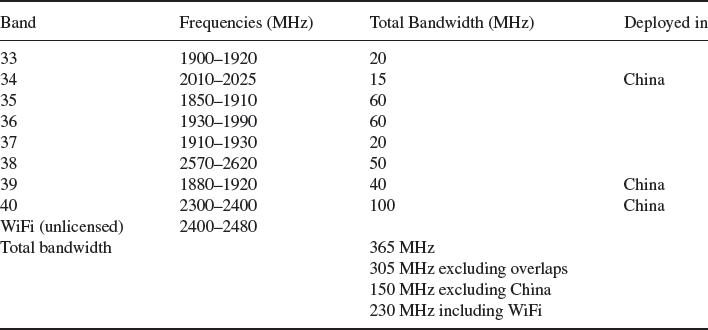
China has pursued its own TDD standards with TD SCDMA and band allocation policy with Band 34 at 2010 to 2025 MHz, Band 39 at 1880 to 1920 MHz and Band 40 at 2300 to 2400 MHz. The assumption is that TDD LTE would also be supported as an option in Bands 38, 39 and 40.
China is one of the few countries with sufficient market scale to support a nationally specific standard and nationally specific band allocations. However, this does not necessarily mean it’s a good idea.
Generally, it can be stated that nonstandard standards and nonstandard spectral allocations have hampered the pace of past progress. The decision by Japanese regulators in the late 1980s/early 1990s to introduce PHS (an alternative to DECT and the UKs ill fated CT2 cordless standard) and PDC, a nonstandard implementation of GSM into nonstandard spectrum at 800 and 1500 MHz was designed to create a protected internal market that could be used by local vendors to amortise R and D and provide the basis for innovation incubation.
In practice, it proved hard to translate this innovation into global markets and the R and D opportunity cost made Japanese handset vendors and their supply chain less rather than more competitive internationally. Korean vendors have faced similar challenges from nationally specific mobile broadband and broadcast standardisation. This has introduced unnecessary opportunity cost without a proportionate market gain.
The decision might alternatively be justified on the assumption that TDD will become more dominant as a mobile broadband bearer but several caveats apply. TDD does not work particularly well in large cells as additional time-domain guard band needs to be introduced to avoid intersymbol interference between transmit and receive time slots. TDD does not work particularly well in small cells as base stations and users within a cell radius are likely to be closer together and therefore more likely to create mutual interference. This will be particularly noticeable with more extreme duty cycles, for example when some users require uplink rather than downlink asymmetry.
As a prior example of this, the three PHS networks deployed in Japan in the mid-1990s were not intersynchronised. PHS networks were also deployed in China, Taiwan and Thailand but never gained an international market footprint. This was partly due to the intersymbol interference issue but also due to the fundamental fact that TDD devices have poor sensitivity. Power in transmit devices does not disappear instantaneously and substantial residual power can still be visible within the RX time slots. This does not matter when the duty cycle is relatively light, for example in a basic GSM voice path where only one slot in eight is transmitting. It certainly matters if the TX duty cycle is high, which in many mobile broadband cases it will be and/or if high peak data rates are supported. If the asymmetry is changing rapidly over time the signalling bandwidth will also become disproportionate.
So in practice, any theoretical gains available from TDD will disappear in implementation loss. TDD may provide higher headline peak data rates but the average data throughput will be lower. TDD next to a LTE FDD receive channel will also be particularly bad news both at the network level, base station to base station, and in the user equipment receive path. Given that it is unlikely that FDD will disappear for the foreseeable future, most user equipment will need to be dual mode, so any potential component savings, eliminating duplex filters for example, would not be possible. Although the RF specifications are similar they are not the same and will incur additional conformance test time and cost. As always, the impact on user equipment cost and performance tends to get overlooked or ignored.
Even at the system level it is arguable whether there is any efficiency gain. The argument is that if the uplink is lightly loaded in an FDD system then valuable bandwidth is being wasted. However, all that happens is that the noise floor at the e node B reduces. This improves the performance of all other FDD uplinks in the cell, reducing power drain for all users served by the cell site.
So you might ask why TDD appears to work in WiFi. The answer is that WiFi is only spectrally efficient and energy efficient because it is low power, 10 milliwatts of transmit power from the user’s device rather than 125 or 250 milliwatts in TDD LTE. The occupied channel bandwidth of WiFi at 2.4 GHz is 22 MHz with a channel spacing of 25 MHz within 80 MHz of operational bandwidth so that’s three channels within 80 MHz. This is not in itself efficient. The efficiency comes from the channel reuse that is in turn a function of the low transmit power. There is some trunking gain achievable from a 20-MHz channel but much of this disappears if bidirectional differentiated quality of service needs to be supported.
It is hard to avoid the conclusion that TDD at least for general use within licensed spectrum is one of those technology cul de sacs that the industry has managed to drive into with no reverse gear engaged. The combination of reasons outlined above explain why wide-area TDD WiMax networks never performed as well as expected as offered traffic loading increased over time.
Anyway, back to FDD. As we have said, in an FDD band plan the bands are subdivided into transmit and receive duplex pairs. The duplex separation varies between 45 MHz (800/850/900 MHz bands) and 400 MHz (Band IV US AWS). The lower duplex in 2007 was always mobile transmit as the propagation conditions are more favourable. However, five years later the allocations are a mix of standard and reverse duplex for reasons that we discuss in Chapter 5.
4.3.2 Band Allocations, Guard Bands and Duplex Separation. The Impact on Transceiver Design, Cost and Performance
The choice of frequency, the guard bands between band allocations and the duplex separation of the uplink and downlink within each individualband all have a profound influence on the architecture of the phone and the active and passive devices used in the phone. Additionally, legacy spectral allocations may need to be supported in some handset frequency plans and future repurposed UHF TV allocations other than the 700 and 800 MHz bands may need to be accommodated.
These ‘wide-area’ cellular radio transceiver functions may also need to physically coexist with local area (WiFi) and personal area transceivers and with easily desensitised receive only functions such as GPS or ATSC/ DVB TV. Digital filtering techniques and architectural innovations, for example direct conversion receivers, translational (GSM) and polar loop (EDGE and WCDMA) transmit architectures, have been developed that minimise the present RF component count and RF component cost implications of multiband and multimode handsets. As a result, it would be reasonable to assume that RF component costs represent a declining percentage of the BOM of a modern cellular handset.
However, RF costs have remained relatively stable as a percentage of the total BOM over time and are likely to remain so. This is due to the increase in RF complexity. It might have also been expected that operator and user expectations of RF performance and functionality, for example higher average data rates would also have encouraged more highly specified RF front ends, but this has not been the case.
Figure 4.14 gives an indication of the typical value split between functions in 2007, in this case in an ultralow-cost handset.
Figure 4.14 The RF BOM compared to other components 2010. Reproduced from RF Cost Economics for Handsets May 20072
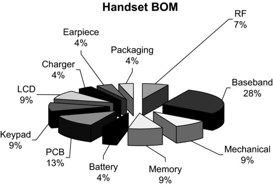
We have said that the RF BOM is staying relatively constant over time as a percentage (between 7 and 10%) of the overall BOM of the phone and that this is true irrespective of whether the phone is an entry level, mid-tier or high-end device.
There are exceptions to this. A mid-tier camera phone in 2007 for example had a value split of about 5% for the RF (including Bluetooth). The logic and digital circuits accounted for about 30%, memory at 12%, the LCD at 10%, the camera at 11%, PCB and electromechanical components at 13%, mechanical components at 14% and ‘other bits’ at 6%. It could be argued of course that the imaging bandwidth of this device would have deserved a more highly specified RF functionality. It is, however, true that a need to support additional access technologies will introduce additional costs.
These costs include nonrecurring expenditure (NRE) and component cost. This implies that volume thresholds are needed to support a supply of handsets that can be considered to be ‘cost economic’ in terms of RF-related NRE and RF-related component cost.
In 2007 it was clear that this volume threshold was higher than generally acknowledged by many in the industry and was increasing over time. In addition, it was hard to achieve competitive RF performance unless certain volume thresholds were achieved. This implied that ‘performance volume thresholds’ and related ‘performance scaling effects’ needed to be factored in to spectral valuation and spectral allocation policy.
It also highlighted the escalating cost and risk factors associated with geographically specific nonstandard spectral allocations, particularly in countries with relatively small addressable markets. These cost and risk factors were compounded by the implementation of nonstandard technologies. This explains why five years later, despite a large expansion in band allocations globally, most phones only support at most four or five bands and at most two wide-area radio access standards, typically GSM and WCDMA.
Any discussion of the economics of adding an additional frequency band to a handset therefore has to comprehend the technology or technologies used to access that band. The technology used (GSM and/or GSM/UMTS in 1997 or GSM and UMTS/LTE in 2012) influences the RF architecture of the phone, the RF component cost of the phone and the nonrecurring engineering cost of getting that phone to market.
It was of course possible to produce UMTS only devices and such devices were developed and sold into some markets, for example Japan. Similarly today, there are iPhone products for the US market that are dualband and some LTE-only dongles. There is little point in adding additional bands if additional cost is incurred.
Additionally, each extra band incurs additional insertion loss and loss of band-to-band isolation. The same applies to multiple technologies. On the other hand, a dualband or single-band single-technology phone can only be shipped to a small local market and will have limited global roaming capability though this only matters to people that regularly travel (less than 10% of the global population).
The 2007 study assumed seven handset categories each supported by a specific band plan. This is shown in Table 4.6.
Table 4.6 Assumed future spectrum allocations by technology in 2007
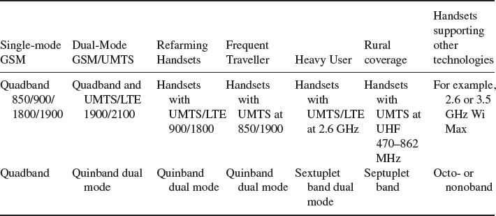
This excluded the probable need to support Band IV in the US (the AWS band at 1700/2100 MHz where T Mobile was the dominant spectral investor) and possible need to support Band VI (800 MHz) and Band IX (1700 MHz) for Japan but there was a general assumption that somehow a world phone would be produced that would cover ten bands or so and multiple access technologies. Such a phone could be shipped to multiple markets and thereby achieve global-scale economy. The devices were commonly and erroneously described as software-defined radio.
4.3.3 Software-Defined Radio, WiMax and the 2.6-GHz Extension Bands
Five years later WiMax has failed to achieve global scale and is therefore no longer on most user equipment vendor development road maps and software-defined radios still do not exist or more specifically the RF functions are still implemented with discrete components.
The 2.6- and 3.5-GHZ bands remain unallocated and unauctioned, though this may have changed by the time most of you read this. What has happened instead is that the top of the UHF TV bands have been allocated and auctioned in the US at 700 MHz and in Europe at 800 MHz. In addition, AT and T has purchased T Mobile in the US to consolidate the AWS band with AT and T 700 and 850 MHz spectral investments, and most phones are still four or five band at most.
It was actually clear to quite a few people in 2007 that software-defined radios would only become available at mass-market prices and mass-market volumes as and when specific device and integration issues were resolved and as and when there were clear financial incentives to realise such a device.
In practice, each additional band whether ‘standard’ (as defined by 3GPP) or ‘nonstandard’ (a country-specific allocation not referenced by 3GPP) incurs substantial nonrecurring investment cost and (related) component cost multipliers.
The market volumes needed to economically cost justify additional band support and/or technology support are substantial and are increasing over time. In 2007 we stated that sufficient market volumes were unlikely to be achieved in any countries or regions other than China, India, Europe and possibly the USA/Latin America. Even in these ‘large local markets’ the entry costs and risks of nonstandard bands were in practice much higher than generally acknowledged. Take intermodulation as an example.
4.3.4 Intermodulation
Whenever two or more frequencies are mixed intentionally or unintentionally within a handset, they will produce sum and difference frequencies. This is known as intermodulation and can occur at receive frequencies and transmit frequencies or between transmit and receive frequencies. Frequencies are mixed or multiplied together intentionally within the frequency synthesiser to create new wanted frequencies to be modulated. The unwanted sum or difference frequency (the image) is filtered out.
When frequencies mix together unintentionally, sum and difference products may translate unwanted signal energy into other bands within the phone or into other proximate devices. A new frequency band introduced into a handset will create a new set of intermodulation products that will need to be managed in terms of their potential impact on the other bands and radio systems used in the phone. Resolving these issues adds to the nonrecurring engineering cost, may result in time to market delay and may add to component cost if additional filtering or reciprocal mixing has to be introduced.
4.3.5 The Need to Support Higher Frequencies and Linear Power Efficiency
The new extension/expansion band at 2.6 GHz and bands at 3.5 GHz creates new challenges. Many countries have legacy wideband radar systems at 2.6 GHz that are problematic but the 2.6 GHz transceivers also have to work with WiFi transceivers at 2.4 GHz These are low power devices, generating not more than 10 milliwatts of transmit power.
Wide-area cellular systems require handsets to transmit at higher powers, typically 250 milliwatts, and to be able to reduce this output power in defined steps down to a few milliwatts (the dynamic output power range over which the phone has to operate).
Handset vendors have a choice of power-amplifier technologies that are typically either based on CMOS (complementary metal-oxide-semiconductor) or SiGe (silicon germanium) or GaAs (gallium arsenide) semiconductor processes.
Simplifying a rather complex story, CMOS is lower cost and supports more aggressive integration but does not perform as well as GaAs particularly at higher frequencies. SiGe combines some of the advantages of CMOS and GaAs. GaAs also has some advantages in terms of delivering a better linearity/amplifier efficiency trade off, an important metric for UMTS and LTE and related technologies using a combination of phase and amplitude modulation. The requirement specifically is to deliver good linearity and efficiency at maximum power and good efficiency at minimum power.
An optimum PA (power-amplifier) technology choice for 3.5 GHz is unlikely to be the same as an optimum PA technology choice for 700 MHz. As a general rule, it gets harder to deliver gain without introducing excessive noise as frequency increases. An optimum PA technology choice for GSM is unlikely to be the same as an optimum PA technology choice for UMTS that requires more linearity to preserve the AM (amplitude-modulation) characteristics in the modulated signal envelope.
Table 4.7 Linearity requirements by technology
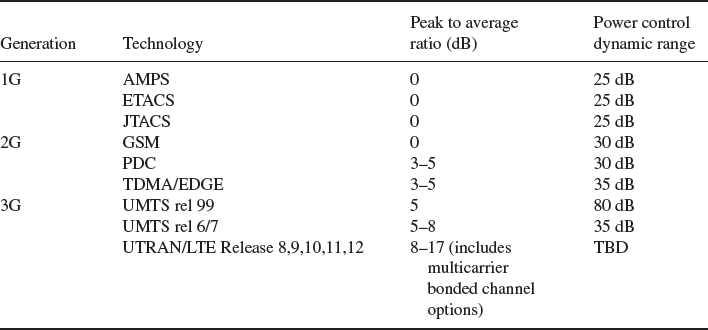
Table 4.7 shows the overall trends over the past 20 years (first- and second-generation cellular) and likely trends over the next five to ten years in terms of the peak to average ratio of the modulated signal envelope (which determines the amount of linearity needed in the amplifier) and the power control dynamic range (which determines the upper and lower power outputs required from the device).
GSMK was chosen for GSM because the modulated signal envelope has no intentional amplitude modulation and could/can therefore use Class C amplifiers (as used in FM analogue systems) albeit with an increased dynamic range (lowest to highest output power). These power amplifiers could be/can be up to 55% efficient. All other evolving technology options including evolved variants of GSM (EDGE) have used/use a combination of phase and amplitude modulation to modulate the signal envelope.
This requirement combined with a wide dynamic power control range has created a number of optimisation challenges for GSM EDGE and UMTS/LTE handsets in terms of RF power efficiency and linearity. Various techniques have been developed that take out the envelope modulation and reintroduce it after signal amplification has been achieved by the PA. These are known variously as polar modulation and/or translational loop architectures and are part of a family of post distortion and predistortion feedback and feedforward techniques that correct for amplifier nonlinearity. These techniques work well but require careful calibration or tracking of RF PA behaviour and the adaptive circuits under varying load characteristics and over temperature and time. In parallel, some of the dynamic range requirements have been reduced by implementing adaptive coding schemes and adaptive modulation schemes that will ease some of these RF PA characterisation issues.
It is therefore important to consider what technology or mix of technologies will be used in the allocated spectral band. Choosing a new nonstandard band for network deployment or failing to mandate a technology for a specific band can have major implications on both the design and function of the RFPA including cost and RF performance (efficiency and linearity). Efficiency loss translates directly into a decrease in talk time. Insufficient linearity translates into a loss of modulation accuracy at high power that will cause a loss of uplink throughput and potential interference to other users.
Power amplifiers can be designed to work over large frequency ranges, for example from 150 to 2500 MHz, but this does not mean that they are necessarily the best choice of technology across the band or have the capability of being acceptably efficient across the band. It is not just the availability of the PA that is important but the filter and matching components needed to make it work efficiently both in the chosen band and across the other bands also supported by the handset.
Power-amplifier pricing in the public domain is often based on relatively small minimum-order quantities, for example 10 000 units. However, these volumes assume multiple customers are likely to be available that will meet and exceed this MOQ criteria. If this looks at all doubtful, or if better returns look achievable from other applications, then the products just will not appear.
Similar design issues need to be considered when validating device performance in multimode handsets where more than one RF PA may be operating simultaneously, for example a (relatively high power) LTE PA generating signal energy in parallel and proximate to a (relatively low power) Bluetooth and/or WiFi transmitter.
This is directly relevant to handsets using a mix of ‘other technologies’. The transmitted signals need to be kept apart from each other and frequency plans need to be carefully validated to prevent intermodulation/mixing of these multiple transmit frequencies both into other transmit bands and into the receive bands supported in the handset. The receive bands could easily desensitise receive functions such as GPS or a DVB T or ATSC receiver. The resolution of these issues can incur substantial nonrecurring engineering cost that need to be recovered in the RF BOM and/or absorbed over substantial market volumes.
If RF functions in the phone are used in an either/or mode rather than simultaneously, there will be a need to ‘mode switch’ in the front end of the phone to provide a dedicated signal path for a particular service. Thus, the choice of a nonstandard band may have an impact on the performance of other radio transceiver functions in the phone but will also require additional components.
There can be several switching functions in the front end of the phone.
4.3.6 The TX/RX Switch for GSM
There may (probably will) be a TX/RX switch that provides a time-duplexed separation between the GSM transmit burst and the receive burst received after a ‘two-slot’ delay (just over a millisecond).These devices will be switching at the frame rate (217 frames per second) and are designed to be reliable over 100 billion cycles or more. The switch speed and duty cycle of these functions makes them presently unsuitable for other technologies, for example MEMS-based switching solutions.
4.3.7 Band Switching
This switch function routes the signal to the appropriate SAW diplex filter that will band pass the wanted signal energy from that band and band stop unwanted signal energy.
4.3.8 Mode Switching
This switch function routes the signal depending on the modulation and air interface standard being used within the band of interest, for example GSM or UMTS. These band-switching and mode-switching devices need to be efficient (offer low insertion loss). They also need good linearity to preserve the integrity of the amplitude-modulated waveforms used in UMTS/LTE and other third-generation air interfaces and to avoid intermodulation and unwanted harmonics. An increased requirement for linearity implies a larger die size (increased cost) and an increase in insertion loss for these devices. There is therefore both a dollar cost and a performance cost to be considered. These devices are typically GaAs devices, though hybrid CMOS/silicon on sapphire processes are also now available. RF MEMS devices may also provide an alternative option for this function.
4.4 The Impact of Increased RF Integration on Volume Thresholds
The power amplifier is presently a separate device not integrated into the RF IC. This is because it is high power (250 milliwatts is equivalent to 24 dBm into 50 ohms). It generates heat. It has to coexist with received radio signals that can be as low as −120 dBm (0.001 of a picowatt). It has to be isolated from the other mixed and digital baseband signals on the chip.
Single-chip phones may be available within the next two to three years, although some vendors suggest this is significantly overoptimistic. However, the availability of these devices whether sooner or later will increase rather than decrease the volume threshold at which nonstandard RF handset designs become economic.
In 2007 most mobile phone designs had the PA, SAW filters and antenna switch (RF front end components) off chip. The VCO (voltage-controlled oscillator) and synthesiser (quite a noisy device) would have been off chip in earlier designs, but by 2007 were generally integrated. As we shall see in Chapter 5 not much has changed in the succeeding five-year period. Partly this is due to the NRE costs and risks of aggressive integration.
The development time and development cost for a retuned integrated receiver rises nonlinearly with integration level. The mask costs are higher; typically about 1 million dollars for a 0.13-micrometre process and increased with integration level as the industry transitioned to 90 and 65 nm.
‘Single-chip’ phones do not make it easier, but rather make it harder to support nonstandard frequency allocations. To realise a truly frequency agile single-chip device requires the integration of diplexing and duplexing onto the die. MEMS-based tuneable filters provide an opportunity to integrate these remaining front-end components on to the RFIC. This provides the basis for a software-defined radio but such products are not presently available at mass-market volumes or mass-market prices.
Integration of these functions onto a device with significant temperature variations will be a particular challenge and it is likely that most if not all vendor solutions will continue to support off-chip RF power amplification in order to ensure device reliability and performance consistency. Even as and when these RF PA and RF MEMS integration challenges are resolved, there will still be frequency-specific components that have to be added to the device, for example the antenna and passive components to match the antenna to the RFIC.
Although MEMS-based functions integrated onto/within an IC potentially offer an ability to have tuneable functionality across a wide range of frequency and band allocations, there will be optimisation limitations. For example, a highly integrated RFIC would be optimised to tune across specific frequency bands with specific channel spacing with specific RF signal characteristics. Additional frequency bands may require hardware optimisation of the IC. At this point, an approximately $6 million ‘entry cost’ is incurred. Hence, our contention in 2007 was that the volume threshold for nonstandard band support would increase rather than decrease as integration levels increased.
This holds true for the transition to 90 nm, the transition to 65 nm and for sub-50-nm processes but also this is an RFIC perspective of the world and we have assiduously noted that a lot of RF components are still not included on the RFIC.
In general, it can be said that it is good practice to study the practical present handset cost multipliers and performance issues implicit in nonstandard band allocations and bear in mind, when developing economic models, that present (NRE) entry costs may increase rather than decrease over time.
Other considerations may be significant, for example the mechanical form factor of the device. The present trend towards superslim phones (a height of less than 7 mm) is dependent on the availability of low form factor passive devices (capacitors, inductors, resistors and other resonant components including the antenna) that are specific to the supported frequency bands.
Small volumes (in terms of space) make it proportionately harder to realise antennas that resonate efficiently across widely spaced frequency bands. ‘Small’ market volumes imply a risk that these ‘difficult to design’ components will not be readily available to the handset vendors. In the intervening period between 2007 and 2012 there has been a general market assumption that high peak data rates are needed and that multiple antennas are needed in mobile devices to achieve this. This has compounded the space/volume problem for antenna designers. As antenna volume reduces, operational bandwidth reduces. This decreases total isotropic sensitivity on the receive path and total radiated power on the transmit path and makes the device more susceptible to hand- and head-proximity detuning effects.
But performance is not just a function of physical volume but also of market volume. High market volumes mean that the performance spread of RF components can be more carefully controlled. This can be best described as ‘performance scaling’, the specific market volumes needed to achieve consistent and acceptable RF performance in practical handset designs.
4.4.1 Differentiating RF Technology and RF Engineering Costs
Technology costs are the recurring costs in the device and a composite of the component technologies needed to support the chosen air interface, or interfaces in single-mode, dual-mode and multimode devices. SAW filters for example are one of the enabling technologies used in the RF section of a modern cellular handset. They have a defined function (to achieve selectivity) and an associated cost that may or may not decrease over time and over volume.
Engineering costs are more typically (though not always) nonrecurring in that they are a composite of the engineering time and effort needed to achieve a certain desired result using a mix of available technologies. Nonrecurring engineering costs have to be amortised over a certain production volume within a certain time.
Cost implies risk and risk implies a business need to achieve a certain return on investment (ROI). Thus, the price charged for components and for the engineering effort needed to turn those components into finished product will directly reflect the return on investment criteria.
This return on investment criteria is not static and may change over time. More significantly, the return on investment will be determined by the number of vendors competing to supply components and finished product to a defined market.
If a market is too small in terms of either volume or value then the likely outcome is that the market will be undersupplied both in terms of the number of component vendors and the amount of engineering effort needed to turn those components into cost and performance competitive product. This will inflate realised prices, limit choice and compromise operator time to market.
Additionally, the handsets that are available will probably perform poorly in terms of their RF functionality. This in turn will limit achievable user data rates (capacity) and the data/voice geographic footprint of the network (coverage). As a rule of thumb, every dB of sensitivity or selectivity lost in a handset translates into a required 10% increase in network density to maintain equivalent coverage/capacity. Handset sensitivity and selectivity is therefore directly related to the overall investment and running cost of the network.
The impact of production volume on RF performance therefore needs to be carefully quantified. The metric is not simply volume but volume over time, effectively a ‘maturity threshold’ that has to be reached in order to support an adequate supply of performance competitive price competitive handsets.
So we need to define the ‘volume thresholds’ and ‘maturity thresholds’ needed to achieve a supply of ‘economically efficient’ handsets. Economically efficient handsets are handsets that have reached a volume threshold at which their component costs do not significantly decrease with additional volume. This implies that an acceptable return of investment has been achieved both in terms of component development investment and the engineering effort needed to turn those components into finished competitive product.
However, we are also saying that economically efficient handsets must also have reached a volume and maturity threshold at which handset RF performance is effectively as good as it can be, given the capabilities of the technology used, in other words a maturity performance threshold.
4.4.2 The Impact of Volume Thresholds and Maturity Performance Thresholds on RF Performance – A GSM Example
In 1992, when GSM single-band 900-MHz phones first became available, it was a major design and production challenge to make phones that would meet the basic conformance sensitivity specification of −102 dBm. There were similar problems meeting other RF performance parameters, for example adjacent channel selectivity and phase errors on the transmit path.
Only just achieving the conformance requirement significantly increases production costs. This is because the variation in component tolerances from phone to phone and batch to batch (a function of component volume) will mean that a significant number of phones will fail to pass basic RF performance production tests. This metric is known as ‘RF yield’. There may be limited opportunities to rework and retest devices but essentially a ‘low’ RF yield will translate directly into an increase in the RF bill of materials for those phones that did actually make it through the production test process.
By 1997 (5 years on), two things had happened. First, most vendors had been through two or three or more design iterations. This had delivered more safety margin in terms of designed performance over and above the conformance specification. Secondly, the major vendors had sufficient volume to negotiate with their RF component vendors to tighten component tolerances to reduce the handset to handset and batch to batch differences that had previously compromised RF yield. So in practice, a significant number of handsets were being shipped to market with a sensitivity of around −107 dBm, 5 dB better than the conformance specification. Note that this did not apply to all handsets from all manufacturers and the spread between best and worst handsets was between 3 and 5 dB.
At this point, GSM phones achieved a lower cost point, provided better and more consistent voice quality, longer talk and standby times, additional functionality and a smaller form factor than analogue cellular phones.
Another ten years (2007) and the best handsets could be measured at −110 dBm (static sensitivity). There was still a ‘best to worst’ spread of between 3 and 5 dB between manufacturers and sometimes also between different handsets from the same manufacturer, but essentially GSM handset performance from an RF perspective was as good as it was ever going to get. The ‘best to worst’ spread still existed partly because of device and design differences but also because not all handsets have sufficient production volume to realise a gain in performance.
Note that over this period, design engineers also had to deliver additional band support. Phones were initially single band (900 MHz), then dualband 900/1800 MHz (from about 1995), then triband 900/1800/1900 (from about year 2000), then triband, and then (2005 to 2007), quadband (850/900/1800/1900).
4.4.3 The Impact of Volume Thresholds and Maturity Performance Thresholds – A UMTS Example
The fact that GSM has more or less reached its development limit in terms of RF performance provided one of the motivations for moving to UMTS. UMTS traded additional processing overhead to achieve what can be rather oversimplistically described as ‘bandwidth gain (analogous to the benefits that broad band FM delivered over narrowband AM systems in the 50 years between 1940 and 1990). Bandwidth gain can be translated into more capacity (more users per MHz of allocated spectrum and/or higher data rates per user) and/or coverage.
There are other RF potential costs benefits, for example the wider channel spacing (5 MHz rather than 200 kHz) relaxes the need for channel to channel RF frequency stability. However, similar rules on volume and maturity performance thresholds apply.
In 2002, the first UMTS phones barely managed to meet the conformance specification of –117 dBm.
Figure 4.15 shows the results of reference sensitivity test on four presently available phones (2006/2007). The best device is over 5 dB better than the conformance specification. Note the difference between the best and worst handsets was about 5 dB (the worst handset only just passed).
Figure 4.15 Sensitivity measurements on four UMTS phones. Reproduced with permission of Spirent Communications – originally published in RF Cost Economics for Handsets Study May 2007.3
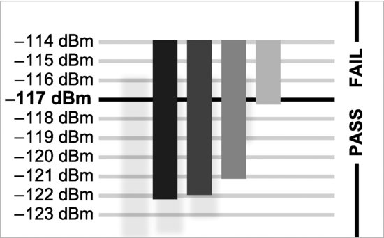
So five years after market introduction, the best handsets available were 5 dB better than specification. In other words both GSM and UMTS handsets improved their sensitivity by 1 dB per year over the first five years of their initial market launch. This improvement has now levelled off to the point where we are as close to the ultimate sensitivity of the device as the existing technology will allow (about another 3 dB) providing justification for the transition to the next generation of technology (LTE).
Note that these performance curves are volume specific, technology specific and frequency specific. The performance gains are achieved by a mix of engineering effort (amortised over significant product volumes) and improved RF component tolerance control. Similar gains over time and over volume are realised in terms of adjacent channel selectivity in the receiver. Similar gains over time and over volume are also realised in terms of transmitter performance, particularly in terms of error vector magnitude, specifically the phase and amplitude accuracy of the modulated signal waveform and the close-in and wideband noise characteristics of the device. An example would be the performance variation from unit to unit of SAW filters over temperature. High market volumes over time gradually erode these device-to-device variations.
Closer tolerancing of active and passive components with volume therefore translates directly into uplink and downlink performance gain. These uplink and downlink gains translate directly into an improved link budget that in turn translates into either higher data rates per user and/or more users per MHz of spectrum and/or improved coverage (a decrease in network density for a given user and data density).
Additionally, as the performance margin improves, RF yield improves, typically from 90% to close to 100%. Note that low RF yield will also choke handset availability, which in turn can lead to significant losses in terms of market opportunity.
These performance benchmarks need to be achieved across multiple bands. Initially most UMTS handsets were designed for 1900/2100 MHz, but as with GSM (the single-band to dualband to triband to quadband transition) UMTS /LTE handsets will need to work equally effectively at 850 MHz, 900 and 1800 MHz, 1700/2100 MHz, at 800 and 1700 MHz in Japan, at 700 MHz at 800 MHz and at 2.6 GHz.
However, as we shall see in Chapter 5, there is a significant risk that LTE devices and parallel HSPA + Release 8, 9, 10 and 11 devices will not follow this positive improvement curve and may well exhibit a far wider best to worst spread than UMTS or GSM. This should be of major concern to all operators or analysts with responsibility for assessing mobile broadband access economics.
As with GSM and UMTS, the addition of each incremental LTE band implies substantial nonrecurring engineering expenditure and small but significant additional component costs in terms of diplex and duplex filter functions. Adding nonstandard bands over and above these presently allocated bands will be problematic in terms of engineering resource allocation (not enough engineers available to do the required design and optimisation work). As we shall see, this explains why vendors work on high ‘opportunity cost’ multipliers when asked to produce handsets for nonstandard bands and/or nonstandard technologies. Additionally, as we have stated, each additional band introduces additional performance loss. It is quite possible that this incremental performance loss will be more significant for LTE devices than for UMTS or GSM devices.
4.5 The RF Functions in a Phone
RF functions in a cellular phone include the selective RF front end, the receiver low-noise amplifier (LNA), RF to IF mixing, the frequency synthesiser and the transmitter power amplifier (PA). The function of the front end is to capture signals of interest on the receive path and to propagate a signal on the transmit path. The receiver LNA amplifies the signal of interest on the receive path.
The mixing process takes the incoming signal and mixes it with a second frequency to create an intermediate frequency (IF) at which the signal will be processed. In direct conversion receivers, the second frequency is identical to the receive frequency but with a 90 degree phase offset.
The frequency synthesiser takes the stability of a frequency reference such as a quartz crystal and translates that reference to the required frequency to be demodulated (receive path) or modulated (transmit path). The transmitter power amplifier amplifies the signal to be transmitted.
4.5.1 RF Device Functionality and Useful Inventions Over the Past 100 Years
For the past 100 years radio devices have been required to oscillate, resonate, filter, switch and amplify. The efficiency with which these tasks are performed defines the overall efficiency of the radio system.
Fleming’s thermionic valve in 1904 and Lee de Forest’s triode valve in 1907 were major moments in radio device development. These devices, combined with resistors, inductors, diodes and capacitors provided the basis for Marconi’s development of tuned circuits during the First World War.
In retrospect, the discovery of the piezoelectric effect by Pierre and Jacques Curie in 1880 was probably at least as significant. The Curie brothers discovered that when pressure was applied to certain crystals, an electrical voltage was generated. Conveniently for the radio industry, this proved to be a bidirectional effect. Applying electrical voltage to certain crystals would cause them to vibrate at a specific frequency.
In 1917, Paul Langevin used quartz crystals in a sonar device for submarine detection and from then on quartz became the basis for detecting and creating specific audio and radio frequencies. In the Second World War, similar research in the US, Japan and the Soviet Union showed that certain classes of ceramics exhibited piezoelectric behaviour. Courtesy of two world wars we were provided with a choice of quartz crystals and/or ceramic-based devices as the basis for providing accurate frequency and time referencing in radio products.
The invention of the transistor in 1947 and the integrated circuit in 1958 used in combination with these devices provided the basis for the power-efficient and spectrally efficient radio transceivers that have powered the wireless industry for the past 50 years and the cellular industry for the past thirty years. However, 50 years on these RF functions are still typically realised as discrete components, existing alongside rather than inside present integrated circuits.
4.5.2 Present-Day Issues of RF Device Integration
Present-day issues of RF device integration are as much mechanical as electrical.
Radio reception starts with an antenna.
Antennas in hand-held devices are either electrical dipoles, small loops, helical, meander antennas or patch antennas. Patch antennas, also known as planar internal antennas are increasingly popular as embedded antennas. Typically, these are used with grounding that shifts the antenna resonance to a lower frequency with a slot added to increase the electrical length, a design known as planar inverted F antennas (PIFA).
Antenna size can also be reduced by using dielectrics with a high dielectric constant. Another option is to use fractal-based antenna patterns to use whatever space is available reasonably effectively. However, any antenna, when constrained within a space that is significantly less than a quarter wavelength of its centre frequency will be inherently inefficient and sensitive to de tuning, for example by hand capacitance effects.
The following are significant contributors to this loss of efficiency.
The imperfect impedance match of the antenna – especially at the band edges – gives rise to significant reflection loss particularly at lower frequencies (850/900/800/700 MHz). Ohmic and dielectric losses convert useful RF energy into heat in the antenna and any associated matching circuits. RF currents may be coupled into other components within the handset, dissipating RF energy inside the phone.
Candy bar, clam shell and slider phones all have similar but different challenges in terms of antenna efficiency. Some antenna designs in present products when used close to the head have negative gains of −8dB or more.
4.5.3 The Antenna TX/RX Switch Module for GSM, Duplexers for UMTS
Another option for improving sensitivity is not to transmit and receive at the same time. This is used in GSM-only phones where there is a two-slot offset between transmit and receive frames. Switching is normally implemented with a GaAs device or pin diodes. WCDMA/UMTS and LTE FDD phones, however, send and receive at the same time, and therefore require a duplexer.
GSM/WCDMA/UMTS/LTE phones therefore typically end up with a duplexer and a GSM TX/RX switch in the front end of the phone. Each additional UMTS/LTE band requires an additional duplexer.
4.5.4 Other Front-End Switch Paths
In addition, there is a need to band switch and mode switch. In an ideal world you would not introduce these switch paths. They create loss and distortion and dissipate power.
More bands and additional modes therefore add direct costs in terms of component costs and indirect costs in terms of a loss of sensitivity on the receive path and a loss of transmitted power on the transmit path.
4.5.5 MEMS Devices
One alternative is to use MEMS (microelectrical mechanical system) -based switches.
The idea of building microelectrical mechanical switches has been around for twenty years or so but is now becoming increasingly practical and has the benefit of sharing available semiconductor fabrication techniques. MEMS components are manufactured using micromachining processes to etch away parts of a silicon wafer or to construct new structural layers that can perform mechanical and electromechanical functions.
A MEMS-based switch would have low insertion loss, good isolation and linearity and would be small and power efficient. In addition, it is essentially a broadband device. It is electrostatically activated so needs a high voltage which is inconvenient, but low current (so practical).
MEMS devices are sensitive to moisture and atmospheric contaminants so have to be hermetically sealed, rather like a quartz crystal. This packaging problem would disappear if the device could be sealed at the wafer level during manufacture with additional overmoulding to provide long-term protection.
Integrated MEMS devices are therefore a plausible candidate for band switching and mode switching within the next three to five years. TX/RX switching (for GSM or other time division multiplexed systems) would be more ambitious due to the duty-cycle requirements but still possible using optimised production techniques. There is also a potential power handling and temperature cycling issue. The high peak voltages implicit in the GSM TX path can lead to the dielectric breakdown of small structures, a problem that occurred with early generations of SAW filters. Because MEMS devices are mechanical, they will be inherently sensitive to temperature changes.
This suggests a potential conflict between present ambitions to integrate the RF PA on to an RFIC and to integrate MEMS devices to reduce front-end component count and deliver a spectrally flexible phone. The balance between these two options will be an important design consideration. The optimal trade off is very likely to be frequency specific.
For example, if the design brief is to produce an ultralow-cost handset, then there are arguments in favour of integrating the RFPA on to the RFIC. However, this will make it difficult to integrate MEMS components on to the same device. You can either have frequency flexibility or low cost, but not both together.
4.5.6 Filtering Using Surface Acoustic Wave (SAW), Bulk Acoustic Wave (BAW) Devices and MEMS Resonators – Implications for Future Radio Systems
These devices are covered in detail in the next chapter but are potentially key enabling technologies.
It seems inevitable that the regulatory environment will require the industry to produce handsets that are capable of working across ever more numerous multiple bands and that the standards-making process will ensure that handsets will also have to support ever more numerous multiple radio standards. This increases RF component cost and makes it harder to deliver consistent RF performance across such a wide range of possible RF operational conditions. This trend also highlights that some of the traditional RF device technologies that have served us faithfully for 50 years or more are nonoptimum for these extended operational conditions.
From a business perspective, there is evidence of a closer coupling between companies with antenna and shielding expertise and silicon vendors. Similar agreements are likely between the MEMS community and silicon vendors to meet the perceived 3- to 5-year need for a closer integration of RF MEMS functionality with next generation silicon. At that stage, but not before, the software-defined radio finally becomes a practical reality. Long-term reliability issues of MEMS devices (given that they depend on mechanical movement) also still need to be resolved.
4.5.7 Handset RF Component Cost Trends
Table 4.8 shows the RF BOM of a Tri Band GSM handset in 2003 (from RTT RF Cost Economics Study for the GSMA September 2007 – original source price points from Plextek4 for the manufactured product costing for a multimedia smart phone designed for a customer.
Table 4.8 Triband GSM RF BOM Reproduced by permission of Plextek
| Component | Quantity | Cost in dollars |
| RF VCO | 1 | 0.94 |
| TXVCO | 1 | 1.6 |
| RF balun | 1 | 0.09 |
| Dual digital transistors | 4 | 0.18 |
| TCVCXO | 1 | 1.53 |
| Triband transceiver | 1 | 2.32 |
| RF front-end module | 1 | 2.19 |
| Transmit power control IC | 1 | 1.08 |
| Triple-band power amplifier | 1 | 2.48 |
| High-speed LDO (2 V voltage regulator) | 1 | 0.11 |
| Total | 12.52 |
The 12.52 dollars equated to 7% of the total BOM cost of $178. The RF PA was the biggest single line item at $2.48. The baseband value was $49.84.
In 2007, a comparative device, admittedly quadband rather than triband would be about 6 dollars costed on a similar volume and the RF BOM would still be about 7% of the total bill of materials. Generally, vendor forecasts in 2007 suggested that the RF BOM cost would halve again to 3 dollars so the RF BOM would be 10% of a 30-dollar handset (for the ultralow-cost handset market) or approximately 7% of a 40-dollar handset. This would only have been achievable if it had been proved feasible to integrate the PA and/or front-end matching in to the RFIC. TI attempted to achieve this, failed, had to write off $250 million of R and D investment and as a result exited the sector that a few years before they had dominated.
Several things happened that in retrospect might seem obvious but were not very evident at the time. The introduction of the iPhone in 2007 raised the realised average price of smart phones, but actually this also meant that the average realised price of phones in general increased rather than decreased on a year-to-year basis.
Inclusion of the iPhone in an operators range plan became and remains a trophy asset and its absence can result in a loss of market value for the operator. Any time-to-market delay therefore assumes a disproportionate importance. This means that the RF design team must choose design and integration options that represent the least risk in terms of time to market delay and the safest way to achieve this is to have relatively unaggressive levels of integration with each separate duplex band having its own discrete RX and TX component and processing path.
This has been great news for the RF component community. A five-band iPhone has (at time of writing at least) five RF power amplifiers and all that implies in terms of component and real estate added value and unit prices are relatively robust due to the high overall value of the handset BOM.
Also, the ultralow-cost handset market never materialised to the extent anticipated. As stated earlier this is partly due to the aspirational effect that smart phones have had on the lower end of the market. Price point expectations in newly dominant markets particularly China are presently aggressive and are linked to a stated need to move rapidly to a 11-band phone. The performance cost of implementing this would be of the order of 7 dB. Even taking low price points for individual components the overall BOM would be substantially higher than most other phones shipped into most other markets.
This makes no commercial sense either for the operator community in China or for the supply chain or for end users who would end up with a phone with poor sensitivity and selectivity that would translate directly into dropped calls and depressingly short voice and data duty cycles.
Poor RF performance would also reduce coverage and absorb operator network capacity and increase customer support costs. However, there is still a conundrum here in that additional bands mean that one phone can be shipped to more markets, thus achieving greater scale gain and savings in inventory management. However, this is more than offset by additional component cost and performance loss.
The Holy Grail is therefore to be able to add bands and/or technologies without additional cost and without performance loss. We examine the practicalities of this in Chapter 5. In the meantime, RF component vendors can breathe at least a temporary sigh of relief as their price point erosion has proved less severe than might have been expected five years ago.
Effectively they have been saved by the smart phone, a device costing $200 rather than $20 dollars selling at $500 rather than $50 dollars with various add on value opportunities of which insurance against damage and loss is bizarrely important.
4.6 Summary
The dynamics of the RF supply chain are complex and occasionally counterintuitive but exhibit the classic gravitational effect typical of large-volume markets with dominant product sectors. In wide-area wireless the dominant legacy technology is GSM. The theoretical spectral efficiency benefits of UMTS/WCDMA might have been expected to encourage a relatively rapid transition from the ‘older’ to newer’ technology, but this has not happened for several reasons. The gravitational effect of the large legacy market has meant that vendors make more money out of innovating for established markets with known volume. The purpose of the innovation is to reduce cost and improve performance. A failure to innovate has an associated opportunity cost. A similar lag effect can now be observed in LTE and will be examined in more detail in the next chapter.
RF innovation has also had to deliver on two fronts – new bands and evolving standards that have become more complex over time. GSM standardisation has moved forward with the introduction of EDGE and higher-order modulation and coding and channel aggregation options. WCDMA has evolved into HSPA and HSPA has evolved into HSPA + and at least partially integrated with the LTE standards road map from Release 8 onwards. Competing standard such as WiMax have further diluted R and D effort.
The impact of this to date is that WCDMA handsets, HSPA handsets and LTE devices have not performed in RF terms as well as they might have done. This has made it harder to realise the theoretical spectral efficiency benefits achievable from the newer technologies. In parallel, there is scant evidence to suggest that energy efficiency on a bit-delivered basis has substantially improved other than as a result of increased network density that incurs additional capital and operational cost.
Once upon a time handset manufacturers and network hardware manufacturers were one and the same. Motorola manufactured handsets and networks, so did Nokia, so did Ericsson, so did Alcatel, even Nortel had a handset division.
One by one these companies either abandoned handset manufacture or decoupled their handset and network development and manufacturing activities. The result is that network equipment and system vendors no longer have control over handset performance. Unfortunately, as we shall see in the next chapter neither do operators. This is an even greater cause for concern.
1 http://www.rttonline.com/resources.html.
