Chapter 6
Power Management of Ultraportable Devices
6.1 Power Management of Wireless Computing and Communications Devices
Cellular telephone technology is one of the best success stories of recent years for its ability to keep the user working untethered for the entire day, with a single overnight recharge. The ultimate vision for this technology is the smart phone, which would have the advanced functionality of a handheld computing device, a digital still camera, a global positioning system, a music player, a portable television set, a mobile phone, and more in a convergent device. Reaching such a level of functionality without compromising the usage model will present enormous challenges as well as opportunities for the electronics industry and in particular for power management.
The Wireless Landscape
The wireless landscape is, and will remain for many years, very fragmented along both geographical and communications standards lines.
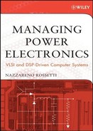
Three generations of digital cellular technologies—second (2G), third (3G), and in-between (2.5G)—already coexist (see Table 6-1).
Japan is ahead of the pack with 3G (W-CDMA and CDMA2000 flavors), while as I write the United States is building the infrastructure to provide 2.5G technology. Europe and Asia are somewhere in between.
Table 6-1 Common Cellular Standards
The Japanese typically do not own home computers and rely increasingly on their phones to exchange text messages as well as access email and the Internet. If this behavior takes hold elsewhere, the future of smart phones is assured.
The real possibility that smart phones will become the next disrupting technology—meaning that the success of smart phones will threaten almost every other established consumer technology, including PCs and notebooks—seems to be confirmed by the recent entrance into the wireless arena of powerful novices like Intel and Microsoft.
Power Management Technologies for Wireless
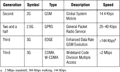
The majority of cellular and handheld devices are powered today by single cell Lithium-Ion batteries. The wireless semiconductor smart ICs in the signal path, following an established industry-wide trend, are mostly designed in sub-micron, low voltage, and high density processes. Consequently the power management ICs are—with a few exceptions—low voltage devices themselves, bridging the gap between the power source voltage range (2.7–4.2 V) and the operational voltage of the signal ICs (1–3.5 V). Such low operational voltages in conjunction with the necessity of low quiescent currents for long standby times have established low voltage CMOS (0.5 μm minimum feature at his juncture) as the process of choice for wireless voltage regulators. Since in these applications the space is premium, these voltage regulators come in very small packages (see Figure 6-1), from leaded to lead-less to chip scale varieties.
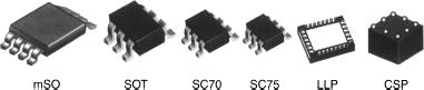
Figure 6-1 Small form factor packages for voltage regulators.
Cellular Telephones
For the next few years, the cellular telephone will remain the dominant wireless device, accounting for 80 percent of total units. Handheld devices and smart phones will account for the remaining 20 percent in roughly equal amounts.
Figure 6-2 shows the typical block diagram of a 2.5G digital cellular telephone, in the class of the T68 mobile phone by Sony Ericsson.
Figure 6-2 Block diagram of 2.5G mobile phone.
Each block requires a specialized power supply. The RF section is particularly sensitive to noise and is best served with low noise linear regulators, while other sections will be served by either linear or switching regulators based purely on architectural and cost constrains.
Figure 6-3 illustrates a possible strategy for the configuration illustrated in Figure 6-2.
The battery can directly power the audio LDO since its output voltage (2.5 V) is below the minimum operational battery voltage (2.7 V). The rest of the LDO outputs fall somewhere inside the battery range of operation (2.7–4.2 V) and consequently, need a higher supply voltage, in this case provided by the boost converter. The DSP core at 1 V will need a dedicated buck converter, while the LCD display contrast at 20 V will need a dedicated boost converter.

Figure 6-3 Power management strategy for a cellular telephone.
Figure 6-4 shows the block diagram of the power management system. In this case, a total of seven voltage regulators are necessary to power this device.
Finally, Table 6-2 shows a wide selection of chips, classified by function, from which to draw for each of the elements in Figure 6-4.
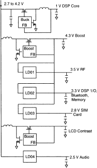
Figure 6-4 Mobile phone power management system.
Table 6-2 Semiconductor Building Block for Wireless Applications

Wireless Handheld
A lot of activity is going into wireless handheld devices, thanks to their potential to intercept and take over a share of the cellular market. Figure 6-5 shows the typical block diagram of a 2G wireless handheld, in the class of the recently announced Palm i705.

Figure 6-5 Block diagram of a 2G handheld computer.
Here again each block requires a specialized power supply, but due to the absence of a DSP and of the SIM card, the power management is a bit leaner than for the case illustrated in Figure 6-2.
With similar considerations to those used for Figure 6-4, Figure 6-6 shows the strategy chosen for the handheld power management and Figure 6-7 shows the implementation, obtained with a total of five regulators.
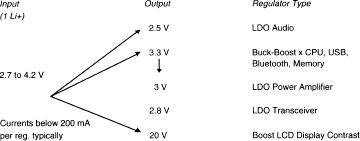
Figure 6-6 Power management strategy for wireless handheld.
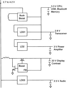
Figure 6-7 Handheld power management system.
Here again the specific components can be drawn from Table 6-2.
Charge
Important elements of both cellular phones and handheld devices are the external AC adapter and the internal charger. Many AC adapters on the market are very simple implementations based on a transformer, a bridge rectifier, and a resistive current limit. More sophisticated controls can be obtained with integrated controllers such as those indicated in Table 6-2.
The Lithium-Ion charger is a constant-current/constant-voltage regulator that is either implemented with specialized controllers (see Table 6-2 for an example) or by PWM of a pass transistor controlled directly by the CPU.
Protection and Fuel Gauging
This section deals briefly with the in-battery electronics, namely that section of power management residing inside the Li+ cell.
Lithium-Ion cells' energy density makes them dangerous elements that need a very precise protocol for charge and handling. Overcharge needs to be prevented as well as undercharge, which leads to reduced energy storage.
To this end, protection electronics measures the battery voltage and opens a pass transistor as soon as the charge voltage threshold is crossed.
Fuel gauging is necessary to be able to display the state of charge of the battery and predict the residual time of operation in battery mode. This is an interesting and challenging feature because residual time of operation matters to the user only toward the end of the battery charge, exactly when the accuracy of the prediction begins to falter. In fact, no matter how precise the measurement system, eventually the residual time of operation will translate into an amount of residual charge that is of the order of magnitude of the system precision, leading to increasing prediction errors as the battery approaches the empty state. This results in the requirement of amazing levels of precision in the current measurement. The measure of current over time is also referred to as Coulomb counting. Analog front-end amplifiers are called to resolve micro-Volts of voltage drops across small sense resistors, followed by 10-bit or higher order A-D (Analog to Digital) converters. The actual processing of the row data today—at the 2 to 2.5G juncture—is generally done in the central processing unit. With 3G systems and above and with smart phones, we expect that the taxing of the DSP—or its successor—will be such that the fuel gauge data processing will be decentralized, leading to smart fuel gauge devices incorporating compact 8-bit microcontrollers.
Figure 6-8 shows an example of an integrated combo fuel gauge and protection control IC that utilizes Fairchild's dual MOSFET FDW2508D as the pass transistor for the protection section.

Figure 6-8 Fuel gauge and protection with FDW2508P as the pass transistor.
Convergence of Cellular Telephone and Handheld
By studying the block diagrams in Figure 6-2 and Figure 6-5, it becomes obvious how similar the two systems are. Both rely on the same radio technologies and frequency ranges, Bluetooth for device-to-device networking, single Lithium-Ion for power source, etc.
In fact, it is easier to point out the differences between the two devices. The DSP, present in the cellular phone only, is a key differentiator allowing for voice processing. Otherwise, it really comes down to size. The handheld typically will have a bigger screen and more memory (Flash memory for operating system, phone book, and files storage and SRAM for temporary data storage) as well as stereo audio for music player emulation (MP3).
A few examples of smart phones, namely handheld devices with DSP on board, already are appearing in the market. One early example is the Blackberry 5810, a handheld PC that can be transformed into a cellular phone by means of a hands-free module connected to the device via a 2.5 mm jack.
As pointed out at the beginning of this chapter, the challenge for the electronics industry is in part technological (will the smart phone be able to deliver the same standby and talk times to which the cellular customers are accustomed?) and in part cultural (will the Japanese model of connectivity illustrated at the beginning of this chapter prevail?).
Future Architectures
At the 3G juncture, the system complexity for cellular and smart phones is such that one DSP is not enough and an additional DSP or ASIC often is necessary to support video and audio compression. In turn, this increases power consumption and reduces battery operation time.
Adaptive Computing Machines (ACMs) are a new class of ICs appearing on the horizon that promise to solve the power dissipation problem by means of a flexible architecture that optimizes software and hardware resources.
Power management in wireless devices is a pervasive issue that encompasses every element in the signal as well as in the power path. With system complexity increasing dramatically from one technology generation to the next, the long duration of untethered operation in wireless devices can be preserved only through the introduction of new breakthrough technologies. New architectures along the lines of the aforementioned ACMs as well as the conversion of large scale ICs from bulk CMOS to Silicon On Insulator (SOI) should go a long way toward reducing the power dissipation of the electronic load. At the other end of the equation, new and more powerful sources of power, such as fuel cells, should be able to provide higher power densities inside the same cell form factor. The entire technology arsenal should be able to continue to provide more features at no compromise.
Power conversion technologies already have achieved impressive efficiencies, reaching peaks of 95 percent. Accordingly, they are a critical element of the power management equation but not its bottleneck. The holdups are at the process and power source levels, and eliminating these bottlenecks will require new process technologies that lead to chips with reduced power dissipation and new power sources with higher power density. The analog building blocks for effective power management of a wireless device in its present and future incarnations are already in place. It is not uncommon today to find these building blocks assembled inside custom combo chips. In this case, such combo chips integrate the entire power management function on board a single IC. Voltage regulators—today designed with 0.5 μm minimum features—will continue to follow the CMOS minimum feature reduction curve, staying only a few technology generations away from the loads they are powering (state-of-the-art 0.13 μm minimum features). Accordingly, they will continue to be able to sustain adequately the power, performance, and cost curve that will be required to power future generations of wireless devices.
6.2 Power Management in Wireless Telephones: Subsystem Design Requirements
Trends in power management are driven by a demand for products loaded with features. Convergent wireless devices, such as smart phones that combine the features of cell phones, PDAs, digital still cameras (DSCs), music players (MPs), and global positioning systems (GPSs), stretch many technology boundaries, including those of power. This section discusses the latest power management products being used in today's most sophisticated cellular phone designs.
Smart Phone Subsystems
A state-of-the-art smart phone system (with handset and AC adapter/charger) can be divided into up to five main board constituents: display board, baseband main board, keypad board, Li+ in-battery board, and AC adapter board. Additional modules may be present for DSC, Bluetooth, or other functions. Accordingly, power management breaks down along these five subsystems. Figure 6-9 illustrates such system partitioning. We will review these subsystems with respect to their power management chips' content, both integrated and discrete, including Light Emitting Diodes (LEDs). These power management chips are:
- LED driver ICs and four white LEDs in the display board
- LED drivers and eight white or blue LEDs in the keypad board
- Power management ICs in the main board
- Lithium-Ion protection and fuel gauge ICs and MOSFETs in the battery pack
- Offline regulator ICs in the AC adapter board
Figure 6-10 shows the corresponding block diagram for a cell phone in the class of Nokia's 7650, which integrates a digital camera.
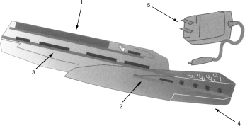
Figure 6-9 System partitioning of a state-of-the-art smart telephone system.
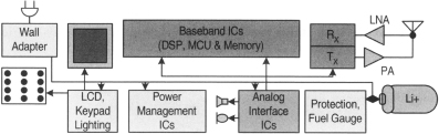
Figure 6-10 Block diagram of a smart phone system.
Display Board
In monochromatic displays, the backlight can be made up of different colors, which generally are obtained with four LED lamps of the same color. In smart phones the color, Thin-Film Transistors (TFT) Liquid-Crystal Display (LCD), necessarily requires only white backlighting. White LED diodes have low forward voltage (around 2.7 V) and require a simple DC current to produce light. Accordingly, a low DC power source (VDD in Figure 6-11) as low as 3.1 V, is necessary to bias these devices. Thanks to such low bias voltage, the four LEDs can operate directly off a single cell Lithium-Ion, the power source of choice in cellular telephones.
A monolithic quadruple LED driver, such as Fairchild Semiconductor's FAN5613 (shown in Figure 6-11), can be housed in a tiny MLP 8-lead package and provide up to 40 mA bias for each diode.
As continuous-time current control may result in poor color consistency, the LEDs can be excited with a pulse width modulated source via the ON/OFF pin to achieve higher color fidelity.

Figure 6-11 Bias scheme for White LED driver with FAN5613.
Keypad Board
Similar to the display configuration, the keypad is also illuminated by LED lamps. In this case, eight white or blue LEDs generally are utilized. For blue backlight, eight QTLP601C-EB InGaN/Sapphire surface mount chip LEDs (shown in Figure 6-12) can be used, with two Fairchild FAN5613 LED Driver ICs driving them.
Figure 6-12 QTLP601C-EB low VF blue LED lamp.
Main Board
The main board contains the vast majority of the electronics, from the baseband DSP and application MCU to the transceiver and analog interface. Each of these blocks is powered by a dedicated voltage regulator. The growing complexity of smart phones requires strict management of the power source. This is obtained by means of a “power manager” inside the baseband processor, communicating to the outside world via logic signals. On the power source side, the voltage regulators are able to receive such logic signals and react accordingly.
In some instances, all the regulator is required to do is to enter into a light load operation or sleep mode or into a shutdown mode via direct logic signals. In other instances, such as in powering the baseband processor, power management is more sophisticated and requires a voltage source that varies with the task at hand, delivering just enough power as necessary and no more. In this case, a voltage regulator, coupled with a D-A converter and a serial bus with the ability to communicate with the host microcontroller, is required. While this technique may sound exotic, such power management schemes are commonplace in notebook computing, battery operated devices that long ago crossed the threshold of complexity that today's smart phones have just now reached. (Examples of popular power management techniques in notebooks are SpeedStep™ from Intel and PowerNow™ from AMD.)
Figure 6-13 illustrates an example of distributed power management on the main board. The combination of a simple buck converter and an SMBus serial-to-parallel interface, such as the FM3570 by Fairchild, allows the CPU to drive the Vcore supply with a 5-bit D-A converter resolution. A combination of switching and linear regulators assures a good compromise between simplicity and performance, and all the devices can be shut down via a dedicated logic pin.

Figure 6-13 Example of distributed power management system for the main board.
Battery Pack
The power management inside the battery pack consists mainly in the Lithium-Ion protection and fuel gauge ICs and MOSFETs. The protection electronics measures the battery voltage and opens a pass transistor as soon as the charge voltage threshold is crossed. Fuel gauging is necessary to display the battery's state of charge and to predict the residual time of operation in battery mode. Figure 6-14 shows an example of in-battery electronics that uses Fairchild's dual MOSFET FDW2508D as the pass transistor for the protection section.
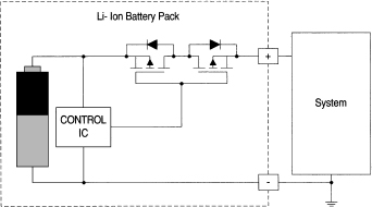
Figure 6-14 In-battery fuel gauge and protection with FDW2508D.
AC Adapter
The AC adapter board rectifies the AC line and converts it down, either to a low DC voltage manageable by the main board, or directly to a constant-current/constant-voltage charging algorithm required by the single Lithium-Ion cell, in which case it performs both the functions of adapter and charger. A charger on the main board will be required only in the first case. In Figure 6-15 the AC adapter/charger is based on an offline switching architecture for the best efficiency. In this example, the high voltage product called the FSDH0165 is powered directly by the AC line and integrates the power into the DMOS transistor for minimum complexity. Later in this chapter, we will discuss in more detail the AC adapter/charger subject.

Figure 6-15 AC adapter for single cell Lithium-Ion.
The power management of state-of-the-art wireless telephones typically breaks down along five main subsystems, each following its own integration dynamics. The main board requires many low voltage sources and lends itself to higher levels of integration. At the opposite end is the AC adapter (or adapter/charger) with its requirement of high voltage (600–800 V) and galvanic isolation with respect to the low voltage side. The keypad board and display can be serviced by the same class of technologies, namely LEDs and LED drivers, while the in-battery electronics is another unique domain where true mixed signal technologies are needed for fuel gauging and protection.
It seems safe to say that the natural boundaries of these subsystems and the diversity of the technologies needed in each of them will assure a plurality of technologies, solutions, and players in the power management of wireless devices.
6.3 Powering Feature-Rich Handsets
Market trends show that devices incorporating color screens, camera phones, and Personal Information Management (PIM) applications are growing steadily. For example, market data by major market research companies like Dataquest and iSuppli point to the possibility that in 2006 the number of smart phones will be larger than the number of the notebook computers shipped that year and will far outnumber single function devices like digital still cameras and PDAs.
With this in mind, we have little doubt that newly emerging applications in cell phones and handhelds, such as video streaming and high quality digital media playback, will soon become legitimate in high-end handsets and will later be embraced by the mainstream.
In this section, we will look at the challenges that such complex devices pose, with a special focus on power management. We will also discuss new solutions and future trends.
Growing Complexity and Shrinking Cycle Time
Today's OEMs play in complex markets, spanning across different platforms—second generation or 2G platforms such as GSM, Time Division Multiple Access (TDMA), and CDMA, and 3G platforms such as W-CDMA and CDMA2000—and each proposed in different models. See Table 6-1 for a review of these acronyms.
For the best time to market, the reference design for a single platform typically will rely on a relatively rigid “core” chipset, while a more flexible periphery will accommodate a model's differentiation within the given platform. In other words, it takes time, sometimes up to a year, to develop new chips that incorporate new features. Consequently a product can go on the shelf faster if it can rely on a rigid core inherently undifferentiated with the differentiation—new features, better performance, etc.—that is accommodated with add-ons. The resulting product may be less integrated and more bulky but goes to market faster. Hence, the final architecture of a product, like the one in Figure 6-16, is influenced by technical factors as well as by time. In the system illustrated in Figure 6-16 the power management—the section of interest for us—is accomplished with a core PMU tightly integrated inside the chipset and an auxiliary PMU servicing the add-on features.
Figure 6-16 illustrates the core chipset, with the baseband section, including the application MCU handling the data, the DSP for voice, FLASH memory, the RF section (with its receiving RX and transmitting TX blocks), and the power management unit section.
A number of add-on modules, such as Bluetooth for untethered data transfer on a short distance, cameras, and LCD modules surround such a core chipset. These blocks require additional power provided by an auxiliary PMU, represented by the PMU add-on block in Figure 6-16.

Figure 6-16 Block diagram of the handset mainboard.
Power Management Unit
The increasing number and performance of smart loads supported by the power management unit demands an increasingly sophisticated PMU, capable of going well beyond providing the basic functions of voltage regulation, charging, and fuel gauging.
In sophisticated systems, the PMU may need to be programmable in order to become platform-specific via software implementation of the protocol. To this end the PMU must be capable of communicating with the host CPU via a serial interface (I2CBus or similar). This is to adjust the power delivery mode to the load demand (heavy, light, or intermediate) and to take responsibility for many critical functions, such as power sequencing, at a time when the communication bus is disabled.
Such PMU can be implemented with varying levels of integration, perhaps initially starting with a solution based on multiple chips for fast time to market, and subsequently up-integrating to a single package (Multi-Chip Package or MCP) or even a single IC, depending on the volumes and other considerations.
Low Dropouts (LDOs)
In Figure 6-17, a microcontroller-based power management architecture provides all the hardware and software functions, as discussed above, in a multi-chip implementation. When defining this unit, many trade-offs need to be considered. The Li+ low voltage (3 V typical) power source is conducive to a high level of integration on standard CMOS. However, this choice hits a snag if a charger, interfacing with an external AC adapter, needs to be integrated, in which case the process technology needs to withstand voltages well above the standard 5 V of CMOS.
Ultimately, if the cost structure allows for its high mask count, a powerful mixed signal BCD process can enable a true single chip solution capable of handling high voltage, high current, and high gate count. As illustrated in Figure 6-17, each subsystem in the handset requires its own specific version of power delivery—low noise LDOs in the RF section and low power LDOs elsewhere. Each subsystem also requires an efficient buck converter for the power consuming processors, a boost converter in combination with LED drivers for the LED arrays, and a linear charger interfacing the Li+ battery with the external AC adapter during charge.
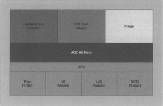
Figure 6-17 Power management unit.
6.4 More on Power Management Units in Cell Phones
The power management of cell phones is one of the most dynamic areas of growth for integrated circuits. Recently, a number of PMUs for cell phone applications have appeared on the market. Handset PMUs range from low integration (single function building blocks) to medium integration (three to ten integrated regulators) to high integration (entire power management, audio power amplifiers, etc.). Interestingly enough, a systematic study of numerous recently released handsets shows no clear trend with respect to levels of integration. Different business models and privileging aspects, from performance to size to cost to time-to-market, explain this fragmented picture. This section focuses on complex PMUs and the capabilities that drive successful product offerings in this area.
Ultraportable devices are feeding the up-integration trend due to shrinking handset dimensions and increasing capabilities such as color displays and the convergence of cell phones with PDAs, DSCs, MP3s, GPSs, and the like. This phenomenon is somewhat similar to what happened in the early 1990s when the shrinking of Hard Disk Drives (HDDs) went from 3.5′′ to 2.5′′ to 1.8′′ and below, which pushed up-integration despite increased costs. In that case, size reduction was paramount (i.e., it didn't matter if the single die would cost more than the dis-integrated solution, due to the inherent lower yield of a bigger die). At that time, many power management companies, lagging on the large-scale integration power process curve needed for that function (Bipolar-CMOS-DMOS), had no choice but to exit the market.
One important difference between the HDDs of the early 1990s and the cellular telephones of today is that, due to its low power and low voltage, the power management IC up-integration in cell phones does not require specialized processes. Instead, this integration can often be accomplished with run-of-the-mill 0.35–0.25 µm CMOS homegrown technology, or with processes easily available at the foundry houses.
Because today's process technology does not appear to be a big barrier, we are witnessing the emergence and participation of fab-less power semiconductor startup companies, a business model not seen before. These are companies with no fabrication facilities that rely on external foundries for chip production. Hence, contrary to what happened with HDDs, we are witnessing an abundance of players at the starting line of the cell phone up-integration race.
Barriers to Up-Integration
The power section in a cell phone, including the power audio amplifiers and charger, is relatively simple; it consists mostly of an array of low-power linear regulators and amplifiers. The complexity comes from managing these functions, which require reliable data conversion and the additional integration of digital blocks such as SMBus for serial communication and state machines, or microcontrollers, for correct power sequencing. Such levels of complexity on board a single die bring their own set of problems, like interference from cross-talk noise.
This new class of power management devices requires technical skills, as well as IP and CAD tools, which go beyond the traditional power team's skill set and cross into logic, microcontroller, and data conversion fields. Such an extension of the capability set in the power management space can be a barrier to entry for traditional analog power companies, while cost competitiveness will likely be a barrier with which the fab-less startups will have to contend.
PMU Building Blocks
Highly integrated power management units are often complex devices housed in high pin count packages. Available devices range from 48 to 179 pins. Such units either can be monolithic, with perhaps a few external transistors for heavy-duty power handling, or multi-chip solutions in a package (MCP). The complexity effectively makes these units custom devices. Because of the custom nature of these units, the following section will discuss the architecture (Figure 6-17) and fundamental building blocks of a PMU in generic terms rather than focusing on a specific device. For the same reasons, building blocks will be illustrated by means of available stand-alone ICs.
Figure 6-17 illustrates a generic microcontroller-based power management architecture, providing all the hardware and software functions, as discussed above. Many trade-offs need to be considered when defining this unit. Some of the regulators, like the charger, are required to provide a continuously rising level of power, which may be difficult to accommodate on board a single CMOS architecture. For example, an external P-channel DMOS discrete transistor, such as Fairchild's FDZ299P, housed in an ultra-small BGA package can help solve the problem. As illustrated in the figure, each subsystem in the handset requires its own specific flavor of power delivery. Low noise LDOs like Fairchild's FAN5234 are used in the RF section and low power LDOs like FAN2501 are used elsewhere. This architecture also requires an efficient buck converter for the power consuming processors as well as a boost converter in combination with LED drivers for the LED arrays.
CPU Regulator
Figure 6-18 shows the die of the FAN5307, high-efficiency DC-DC buck converter; the big V-shaped structures on the left are the integrated P- and N-channel MOS transistors, while the rest of the fine geometries are control circuitry. The FAN5307, a high efficiency low noise synchronous PWM current mode and Pulse Skip (Power Save) mode DC-DC converter, is designed specifically for battery-powered applications. It provides up to 300 mA of output current over a wide input range from 2.5 V to 5.5 V. The output voltage can be either internally fixed or externally adjustable over a wide range of 0.7 V–5.5 V by an external voltage divider. Custom output voltages are also available.
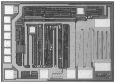
Figure 6-18 FAN5307 buck converter.
Pulse skipping modulation is used at moderate and light loads. Dynamic voltage positioning is applied, and the output voltage is shifted 0.8 percent above nominal value for increased headroom during load transients. At higher loads, the system automatically switches to current mode PWM control, operating at 1 MHz. A current mode control loop with fast transient response ensures excellent line and load regulation. In Power Save mode, the quiescent current is reduced to 15 µA in order to achieve high efficiency and to ensure long battery life. In shut down mode, the supply current drops below 1 µA. The device is stand-alone and is available in 5-lead SOT-23 and 6-lead 3 × 3 mm MLP packages.
Figure 6-19 shows the voltage regulator application complete with external passive components. The integration of the power MOS transistors leads to a minimum number of external components, while the high frequency of operations allows for a very small value of the passives. Appendix D provides the data sheets of FAN5307 for more technical details.

Figure 6-19 FAN5307 application.
Low Dropout Block
Due to the relatively light loads (hundreds of mA rather than hundreds of Amperes as in heavy-duty computing applications), low voltages (one Li+ power source or 3.6 V typical), and often low input-to-output dropout voltages, simple linear regulators are very popular in ultraportable applications. Figure 6-20 shows the die of the FAN2534 low dropout (180 mV at 150 mA) regulator: a state-of-the-art CMOS design that targets ultraportable applications and is characterized by low power consumption, high power supply rejection, and low noise. Here again, the V-shaped structure is the P-MOS high side pass transistor and the rest of the fine geometries are the control logic.
In this section, we have discussed the evolution of complex PMUs in cell phones, illustrating the benefit of using the microcontroller in sophisticated applications such as a handset illumination system. We have reviewed the breadth of mixed-signal technologies and architectures coming into play, focusing on fundamental building blocks of the PMU: the microcontroller, the buck converter, and the LDO. These, and other building blocks like LED drivers, chargers, and audio power amplifiers, can all be integrated monolithically or in multi-chip package form to implement a modern handset power management unit.
From this discussion, it should be clear that the likely winners of the race for the PMU sockets will be the companies with the broadest combination of skills and capabilities to meet the technical hurdles and the stringent cost targets imposed by this market. The successful companies will need to have knowledge of ultraportable systems, power analog and digital integration experience, and the ability to mass-produce these chips.
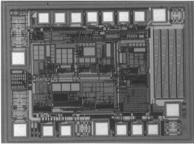
Figure 6-20 FAN2534 LDO die photo.
The Microcontroller
As discussed in the last section, the microcontroller, a block diagram of which is shown in Figure 6-21, is the basis of a feature-rich, or smart phone, power management unit. Fairchild's ACE1502 (Arithmetic Controller Unit) family of microcontrollers, for instance, has a fully static CMOS architecture. This low power, small-sized device is a dedicated programmable monolithic IC for ultraportable applications requiring high performance. At its core is an 8-bit microcontroller, 64 bytes of RAM, 64 bytes of EEPROM, and 2/k bytes of code EEPROM. The on-chip peripherals include a multi-function 16-bit timer, watchdog and programmable under-voltage detection, reset and clock. Its high level of integration allows this IC to fit in a small SO8 package, but this block can also be up-integrated into a more complex system either on a single die or by co-packaging.
Another important factor to consider when adding intelligence to PMU via microcontrollers is the battery drain during both active and standby modes. An ideal design will provide extremely low standby currents. In fact, the ACE1502 is well suited for this category of applications. In halt mode, the ACE1502 consumes 100 nano-amps, which has negligible impact on reduction of battery life. Appendix E provides the data sheet of ACE1502 for more technical details.
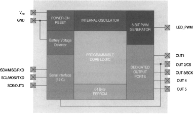
Figure 6-21 Microcontroller architecture.
The Microcontroller Die
The microcontroller is often the basis of a feature-rich, or smart phone power management unit. Fairchild's ACE1502 microcontroller die is shown in Figure 6-22. This IC fits in a small SO8 package, but this block can also be up-integrated in a more complex system, either on a single die or by co-packaging..

Figure 6-22 ACE1502 microcontroller die.
Another important factor to consider when adding intelligence to PMU via microcontrollers is the battery drain in both active and standby modes. An ideal design will provide extremely low standby currents. In fact, the ACE1502 is well suited for this category of applications. In halt mode, the ACE1502 consumes 100 nano-amps, which has negligible impact on reduction of battery life.
Processing Requirements
As the trend continues toward convergent cell phone handsets, development of software and firmware becomes an increasingly complex task. In fact, as the systems tend toward larger displays and the inclusion of more functions, such as 3-D games, a phone's processing power and software complexity drive its architecture toward distributed processing. The microcontroller adds further value in off-loading the power management tasks from the main CPU, thus freeing it to perform more computing intensive tasks.
The application of “local intelligence,” via a microcontroller, can assume various levels of sophistication, such as the recent trend of feature phones. For example, it is common to find phones with digital cameras built into them. However, the lack of a photoflash limits the use of the phone's camera to brightly lit scenes. To address this problem, it is now possible to include a flash unit built from LEDs. The addition of a flash requires several functions such as red-eye reduction and intensity modulation, depending on ambient lighting and subject distance as well as synchronization with the CCD module for image capture. These additional functions can be easily off-loaded to a peripheral microcontroller. Such architecture leads to optimized power management and simplifies the computing load on the main CPU.
Microcontroller-Driven Illumination System
A complex LED based illumination system is illustrated in Figure 6-23. Typically, an array of four white LEDs is needed for the color display backlighting, while another array of four white or blue LEDs implements the keyboard backlighting. White LEDs, typically assembled in a quad package, are needed for the camera flash. And finally, an RGB display module provides varying combinations of red, green, and blue flashes for lighting effects. As mentioned earlier, the sequencing and duration of all the illumination profiles are under micro control.
Figure 6-24 demonstrates the lighting system described previously, with all the elements of the system excited at once. The back light and display light locations are obvious. The flash is the top light and the RGB is the one in the middle.
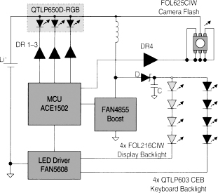
Figure 6-23 Handset illumination system.

Figure 6-24 Lighting system demonstration.
Figure 6-25 shows the typical waveform generated by the microcontroller to drive the lighting system. The oscilloscope waveforms are:
- A1 FLASH LED cathode signal
- A2 primary back light intensity control via 8-bit PWM signal
- 2 secondary back light intensity control via 8-bit PWM signal
- 3 RGB LED Module: Red channel controlled using 4-bit PWM signal
- 4 RGB LED Module: Green channel controlled using 4-bit PWM signal
- 5 RGB LED Module: Blue channel controlled using 4-bit PWM signal:

Figure 6-25 Lighting system waveforms.
6.5 Color Displays and Cameras Increase Demand on Power Sources and Management
One of the most amazing recent trends in ultraportable technology is convergence. With smart phones representing the convergence of PDAs, cell phones, digital still cameras, music players, and global positioning systems. With Audio Video Recorders (AVRs) converging camcorders, DSCs, audio players, voice recorders, and movie viewers into one piece of equipment.
While some of these convergences will take time to materialize in the mainstream, others are improving rapidly. One of these rapidly improving areas is the convergence of two very successful ultraportable devices: DSCs and color cell phones, into a single portable device.
This section reviews the DSC first and then dives into the integration of this function into cell phones. Finally, the implications in terms of power consumption and power sources are discussed.
Digital Still Camera
Digital still cameras have enjoyed a brisk growth in the past few years and today there is more of a market for DSCs than notebook computers. One third of these DSCs are high resolution (higher than three megapixels); today top of the line cameras exhibit close to five megapixels with seven on the horizon.
Figure 6-26 illustrates the main blocks of a DSC and the power flow, from the source (in the example one Li+ cell) to the various blocks.
The key element in a DSC is its image sensor, traditionally a charge coupled device (CCD) or more recently a CMOS integrated circuit that substitutes the film of traditional cameras and is powered typically by a 2.8–3.3 V, 0.5 W source.
A Xenon lamp powered for the duration of the light pulse by a boost regulator converting the battery voltage up to 300 V, produces the camera flash. The lamp is initially excited with a high voltage (4–5 kV) pulse ionizing the gas mixture within the lamp. The pulse is fired by a strobe unit composed of a high voltage pulse transformer and firing IGBT like the SGRN204060.
The color display backlight can be powered by four white LEDs via an active driver like the FAN5613 which allows duty cycle modulation of the LED bias current to adjust the luminosity to the ambient light, thereby minimizing the power consumption in the backlight.
The focus and shutter motors are driven by the dual motor driver KA7405D and the Li+ battery can be charged by the FSDH565 offline charger adapter.
Finally powering the DSP will be accomplished by a low voltage, low current (1.2 V, 300 mA) buck converter.
As an example, the peak power dissipated by a palm sized DSC (1.3 megapixels) during picture taking can be around 2 W and 1.5 W (or 500 mA at 2.4 V) during viewing. Two rechargeable alkaline cells in series with 700 mAh capacity can then sustain close to one hour of picture taking and viewing.

Figure 6-26 Generic DSC and power distribution.
Camera Phones
If DSCs are doing well, camera phones are sizzling. It is expected that soon the number of camera phones will surpass the number of DSCs and by 2007, one forth of all cell phones produced will have integrated cameras.
The Japanese have been leading the demand of high-end camera phones equipped with mega-pixel, solid-state memory cards and high-resolution color displays.
At the time of this writing, a number of camera phones are being announced in Japan with a resolution of 1.3 megapixels, matching, at this juncture, the performance of low end DSCs. Not surprisingly, forecasts for DSCs are starting to exhibit more moderate growth rates.
Cameras for current cell phones are confined inside tiny modules and generally meet stringent specifications, including one cubic centimeter, 100 mW power, and 2.7 V power source and cost ten dollars.
Right now, a big technology battle is going on regarding image sensors. Cell phone manufacturers are willing to allocate 100 mW or less of power dissipation to image sensors. CCDs are currently close to that limit, while CMOS typically require half.
While at the lower resolutions, CMOS image sensors seem to have won out over CCD thanks to their lower power dissipation, at the higher resolutions (greater than one megapixel) CDD is in the lead.
Camera phones that are currently available have resolutions in the 0.3 megapixels range and consume pretty much the same peak power levels (below 1.5 W) in call and picture mode.
Current camera phones, like DSCs, come with 8 to 16 MB memory stick flash memory for storage. The new solid-state memory cards, dubbed Mini SDs (Security Data), will go up to 256 MB by the end of 2005.
Based on the DSC example discussed earlier, a 1.3 megapixel camera phone could exhibit peaks of power consumption in picture mode (2 W) higher than in call mode (1.5 W).
Such state of the art camera phones typically equipped with a 3.6 V, 1000 mAh Li+ cell should warrant up to two hours of call and picture mode.
Figure 6-27 shows the picture of a GSM camera phone main board and Figure 6-28 shows the disassembled battery powering a CDMA2000 camera phone, both courtesy of Portelligent.
The trade-off for all these features is a reduction of the cell phone talk time ability, from six hours for regular cell phones to one or two hours for the new camera phones.
The attacks on talk time will continue as the pressure for a higher number of pixels, higher resolution displays and more features incorporated into the cell phone increases.
With one to two hours of operation, the camera phone finds good company in its bigger relative, the notebook PC: both devices badly in need of new technologies capable of extending their untethered operation time. As both rely on the same display (LCD) and battery (Li+) technologies, it is no surprise that they also suffer from the same problem, namely short operation time in mobile mode. For the notebook to achieve its goal of eight hours of operation and the cell phone to go back to its initial talk time of six hours, we need new technologies to come to bear. Fuel cells, electrochemical devices converting the energy of a fuel like methanol directly into electricity, have the potential to store ten times the energy of current battery technology, and it is likely that they will be ready for prime time in a couple of years.
On the display front, emissive technologies like Organic LEDs (OLEDS) clearly need to take over from current transmissive LCD technology, thereby eliminating the power-hungry backlight outfits. The first OLED display-based camera phone was announced in March of 2003. Since it appears that it is more difficult to produce reliable large sized OLED displays, this technology will probably penetrate the ultraportable market first, before moving to the notebook and beyond.
Finally, it is worth mentioning that White LEDs are moving beyond backlighting applications and enabling the use of flash in phone cameras, thanks to their greater efficiency and simplicity of operation compared to xenon lamps.

Figure 6-27 Camera phone mainboard example. (Courtesy of Portelligent)
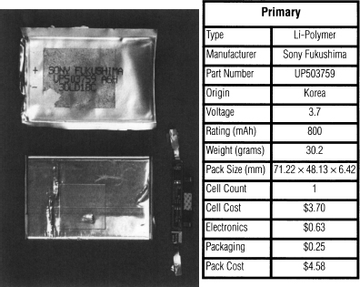
Figure 6-28 Battery and electronics daughterboard disassembled. (Courtesy of Portelligent)
No doubt the convergence phenomenon will continue. If high-resolution displays, cameras, and storage cards have been the drivers so far, no less compelling applications are on the horizon, like video on a handset, GPS, and more.
Fortunately, new technologies are coming along that are capable of both taming the escalation of power consumption (White LEDs, OLEDs) as well as breaking the current bottlenecks (fuel cells).
Is there an upper limit to the power consumption? Higher power consumption translates directly into higher temperatures in the gadgets we all love. Again, look at the notebook for an answer—in the near future we will likely be called to bear in our hands similar temperatures to those that we currently endure from our laptops. We expect then that our handsets will become as hot as possible without crossing the threshold of discomfort, as cooling down is an expensive and bulky proposition.
Power Minimization
The battle for power waste-minimization extends to the signal path as well. The logic gates, operational amplifiers, and data conversion devices used extensively in ultraportable applications are all specifically designed for ultra low power dissipation and are housed in space efficient packages.
For example, the Ultra Low Power (ULP and ULP-A) TinyLogic® devices, such as Fairchild's NC7SP74, a D flip-flop, and the NC7SP00 dual NAND gate, operate at voltages between 3.3 V and 0.9 V and have propagation delays as short as 2.0 ns, consuming less than half as much power as existing high performance logic.
Untethered Operation
Recent high-end handsets exhibit amazing features such as dual color LCD displays, camera, video on demand, and audio on demand. An 800 mAh Li+ battery (corresponding to a 2.4 Wh at 3 V average output) can sustain heavy-duty activities like playing games, taking pictures, or recording and viewing videos—assuming each activity consumes power at a rate of 1.4 W for less than two hours. Such figures of merit are getting better, thanks to the power management methods discussed previously, but they remain a far cry from the desired performance of 6–8 hours of untethered operation as in more basic handsets.
The two technologies on the horizon promising to improve this situation are organic LEDs, which do eliminate the power consuming backlights, and fuel cells; electrochemical devices capable of extracting electricity directly from fuels like methanol. Fuel cells already promise to flank Li+, for example as untethered chargers, and then to progressively substitute Li+ technology.
Alternative power sources, such as fuel cells, will require even more sophisticated power management. This increased management will necessitate further proliferation of local intelligence to manage tasks (i.e. additional microcontrollers,; including sophisticated mixed signal capabilities to perform supervisory functions.
Digital still cameras with OLEDs are already commercially available and this technology is expected to take a wider hold in the next three to five years. Fuel cells are a proven technology but difficult to miniaturize and they may come to larger devices like notebooks before trickling down to handsets. Prototype handsets, some powered by, and others simply charged by fuel cells, have been demonstrated and are expected to become commercially viable in the same timeframe as OLEDs.
Power management techniques are adapting and evolving to keep up with the increased complexities of today's systems. These techniques include traditional cell library regulation elements as well as untraditional digital functions, such as bus interfaces, data converters, and microcontrollers.
Feature-rich handsets and smart phones are clearly the devices pushing the edge of every technology, including power, and more features will be coming in the future. For example, it is conceivable that a series of “plug and play” standards will be debated and then adopted to allow for mix-and-match of add-on peripherals (camera, GPS modules, etc.) from various sources, as well as promote the re-use of peripherals that a user already owns. The addition of microcontrollers in power management applications will become an increasingly important theme in the ICs that provide system power for these platforms.
This “smartening” of power management electronics, combined with the increasing maturity of new technologies for energy storage and displays, promises to keep these feature-rich devices on a steep growth curve for the foreseeable future.