Chapter 7
Computing and Communications Systems
7.1 Power Management of Desktop and Notebook Computers
Power management of PCs is becoming an increasingly complex endeavor. Figure 7-1 shows the progression of Intel PC platforms, from the launch of the Pentium in 1996 to current times. The Pentium brand CPU opens up the modern era of computing however, the birth of the CPU goes back as far as 1971 to the Intel 4004 CPU. In Figure 7-1 below each Pentium generation and associated voltage regulator offered by Fairchild Semiconductors, we find the year of the platform launch, the voltage regulation protocol (VRMxxx), the minimum feature (minimum line width drawn) of the transistors at that juncture in micro-meters, and the current consumption of the CPU.
Before Pentium, CPUs required relatively low power and could be powered by linear regulators. With Pentium the power becomes high enough to require switching regulators, devices distinctively more efficient than linear regulators. With Pentium IV the power becomes too high to be handled by a single phase (1Φ)—just to grasp the concept, think of a single piston engine trying to power a car—regulator, and the era of interleaved multiphase regulation (the paralleling and time spacing of multiple regulators) begins. At the VRM10 juncture, the breath-taking pace of Moore's law has slowed down somewhat, as exemplified by the unusual longevity of this platform. At the VRM11 juncture, the rate of increase in CPU power consumption has been slowed down with sophisticated techniques such as back biasing of the die substrate, to reduce leakage, new dielectric materials to reduce switching losses and strained silicon, a technique that stretches the silicon lattice resulting in wider passages for the electrons and hence lower ohmic resistance. In the following session we will discuss first a Pentium III platform, covering most of the basic power management technology needed for the PC. Then we will cover a Pentium IV platform, focusing on new features specific to this platform, such as interleaved multiphase and extending the discussion to notebook systems as well.

Figure 7-1 Progression of CPU platforms according to Moore's law.
Power Management System Solution for a Pentium III Desktop System
In this section we will review in detail the power management for a Pentium III system, while in the next section we will focus on Pentium IV. With PIII, the PC power management reaches a very high level of complexity in terms of power management architecture. The subsequent PIV platform doesn't change much except for the fact that more powerful CPUs require more hefty CPU voltage regulators.
Nine Voltage Regulators on Board
With the PIII platform the motherboard needs nine distinct regulated voltages, none of which are directly generated by the ATX silver box and all of which consequently need to be generated locally on the motherboard. The voltage types are as follows:
The Main Derived Voltages
These voltages all come from the 5 V silver box or 3.3 V silver box Mains
- DAC controlled CPU voltage regulator
- 2.5 V clock voltage regulator
- 1.5 V VTT termination voltage regulator
- 3.3 V or 1.5 V Advanced Graphics Port (AGP) voltage regulator
- 1.8 V North Bridge (now renamed Micro Controller Hub or MCH) voltage regulator
The Dual Voltages
The dual voltages are managed according to the ACPI (Asynchronous Computer Peripheral Interface) protocol and powered from the silver box Mains during normal operation, or from the silver box 5 V standby during “suspend to RAM” state.
- 3.3 V Dual voltage regulator (PCI bus power)
- 5 V Dual voltage regulator (USB power)
The Memory Voltages
Memory voltages turn off only during “soft off' state.
- 3.3 V SRAM voltage regulator
- 2.5 V RAMBUS voltage regulator
The motherboard is becoming too crowded to be able to make room for nine separate power supplies. The best architecture is one in which the number of chips, and consequently the total area occupancy, are minimized. Figure 7-2 shows an architecture in which four of the five Main derived voltages are controlled by a single chip, while the four ACPI voltages are controlled with a second chip (effectively a dedicated quad linear regulator with ACPI control). The ninth regulator (North Bridge regulator) is provided separately for maximum flexibility.
The CPU Regulator
The CPU regulator is by far the most challenging element of this power management system. The main tricks of the trade employed to deliver high performance with a minimum bill of materials are discussed in detail in this section, including the handling of ever increasing load currents and input voltages in conjunction with decreasing output voltages, voltage positioning, and FET sensing techniques.
The Memory Configuration
Intel's recommended configuration for memory transition from SDRAM to RDRAM is 2 RIMM modules and 2 SIMM modules—this points clearly toward an architecture for the ACPI controller in which both RAMBUS and SRAM voltages are available at the same time, as opposed to an architecture in which a single adjustable regulator provides one or the other.
The RC5058 + RC5060 power management chipset shown in Figure 7-2 is proposed as an example of a complete motherboard solution.

Figure 7-2 Pentium III system power management.
Power Management System Solution for Pentium IV Systems (Desktop and Notebook)
This section reviews the main challenges and solutions for both desktop and notebook PCs.
Introduction
Personal computers, both desktop and notebook, play a central role in the modern communication fabric and in the future will continue that trend toward a complex intertwining of wired and wireless threads (Figure 7-3) all contributing to the ultimate goal of computing and connectivity anywhere anytime.

Figure 7-3 PCs and notebooks at the center of the communication fabric
To make the challenge even more daunting, this goal must be accomplished in conjunction with another imperative, “performance without power dissipation.”
This chapter focuses on the latter challenge. Today's state-of-the-art technology is illustrated through the discussion of power management for a desktop system and a notebook system. We will also discuss future trends toward the achievement of both goals mentioned above.
The Power Challenge
Moore's law has two important consequences regarding power:
It creates a technology hierarchy with the CPU at the top, produced with the smallest minimum feature (today 0.13 µm) and requiring the lowest supply voltages (1-1.5 V) available thus far. Consequently, the previous CPU generation infrastructure for 0.18 µm gets recycled down the “food chain” for memory, which is powered at voltages around 2.5 V. The cycle goes on and on with lower minimum features and lower voltages continuously generated. The end result is a downward proliferation of power supply voltages from 5 V down to 3.3 V, down to 2.5 V, down to 1.5 V, etc. This phenomenon fuels the proliferation of “distributed power.” Every new generation motherboard has more functions and requires more voltage regulators than the previous one, while at the same time the motherboard form factor is shrinking to meet the new demands for slick form factors.
By stuffing more and more transistors in a die (a Pentium IV CPU in 2004 has 42 million transistors versus 2300 transistors in 1971 for the Intel 4004 CPU) modern devices create tremendous problems of heat and power dissipation which must be resolved by us, the power specialists. This phenomenon has generated a tremendous migration from inefficient power architectures like linear regulators (believe it or not, the first CPUs were powered by Low Drop Output regulators, or LDOs, notorious for their high losses) to more efficient ones like switching regulator architectures. The workhorse for switching regulators continues to be the buck, or step down converter, continuously renewing itself into more powerful implementations, from conventional buck to synchronous to multiphase, in order to keep up with the CPU growing power.
Both trends compound the same effect, a phenomenal concentration of heat on the chips and on the entire motherboard that cannot continue untamed. More on this subject will be discussed later.
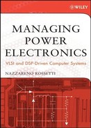
Desktop Systems
Figure 7-4 and Figure 7-5 illustrate a modern desktop system in its main components: the microprocessor, the Memory Channel Hub (MCH, also referred to as North Bridge), and the I/O Hub (IOH or South Bridge), connecting to the external peripherals. While the silver box can only provide the “row” power (5 V, 3.3 V, and 12 V), most of the elements in the block diagram need specialized power sources, to be provided individually and locally. Going from wall to board, an impressive slew of processes and technologies come to bear, from high voltage discrete DMOS transistors to Bipolar and Bi-CMOS IC controllers, from power amplifiers to linear and switching regulators. They all fall under a centrally orchestrated control providing energy in the most cost effective and power efficient way possible.
Powering the CPU
By far the most challenging load on the motherboard is the CPU. The main challenges in powering a CPU are:
Duty Cycle
High input voltages (12 V) and low output voltages (1.2 V typically) for the regulator, leading to duty-cycles of 10 percent (VOUT/VIN = 0.1). This means that useful transfer of power from the 12 V source to the regulated output happens only during 10 percent of the time period. For the remaining 90 percent of the time the load is powered only by the output bulk capacitors (tens of thousands of microFarads).
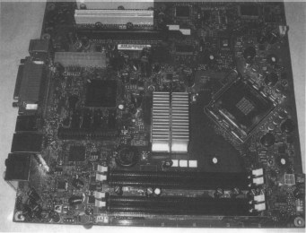
Figure 7-4 Desktop PC motherboard.
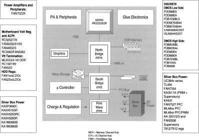
Figure 7-5 Desktop system.
So far, the introduction of interleaved multiphase buck converters has helped reduce the number of both input and output bulk capacitors. Still, the amount of capacitors used today is huge and the current trend is racing toward faster architectures and technologies capable of reducing the size of the passive elements without compromising the efficiency of the regulator, which must remain near 80 percent. This efficiency requirement also puts the discrete technology on the front line: it will take a new generation of discrete DMOS transistors with sensibly lower switching losses to achieve this goal. The desirable endpoint is elimination of electrolytic capacitors—the current workhorse of bulk capacitors—in favor of an all-ceramic solution.
Tight Regulation
Output voltage is tightly regulated. The voltage across the CPU is allowed to vary over production spreads and under wide and steep load transients (30 A/µs) for only a few tens of millivolts.
One industry standard practice, in order to alleviate the problem of eating up the voltage margins due to voltage spikes during load transients, is the utilization of a controlled amount of output “droop” under load. The waveform in Figure 7-6(a) shows the normal behavior of a regulated output in absence of droop, exhibiting a total deviation of 2 × ESR × I, where I is the current and ESR is the series resistance of the bulk capacitor C. By adding a droop resistor RDROOP in the indicated position and of value equal to ESR (RDROOP = ESR) the total deviation is reduced to ESR × I as the (b) waveform illustrates. It follows that the waveform (b) will have a total deviation equal to the waveform (a) at twice the ESR value, corresponding to half the amount of output bulk capacitors. The technique has been illustrated here with passive droop via RDROOP. Since passive droop is dissipative, the best practice is to do “active droop” or drooping of the output by controlled manipulation of the VRM load regulation, yielding the desired reduction in BOM at no efficiency cost. Finally, as the output voltage droops under load, less voltage and proportionally less power is delivered to the load, leading to a sensible reduction in total system power dissipation.
Dynamic Voltage Adjustment
Dynamic voltage adjustment of the output is done via D-A converter on the order of hundreds of nanoseconds to accommodate transitions to and from low power modes.
Our architecture, valley control, exhibits a very fast transient response and hence fits this type of application very well.
Figure 7-7 illustrates valley current-mode control based on leading-edge modulation. The error amplifier forces VOUT to equal VREF input. However, contrary to the standard peak control technique, now its output voltage, Vε, is compared to the low-side MOSFETs current (IL) times RDSON. When IL × RDSON below the error voltage, the PWM comparator goes high. This sets the flip-flop, initiating the charge phase by turning on the high-side driver and terminating the discharge phase by turning off the low-side driver. The charge phase continues until the next clock pulse resets the flip-flop, initiating a new discharge phase. The advantage of this architecture is that it easily senses the current on the low side driver, where the current is present for 90 percent of the time in a 10 percent duty cycle application like this. For example if the clock frequency is 300 kHz, the high side pulse is only 330 ns, whereas the low side pulse is 2.97 µs. Consider also that sensing a 330 ns pulse on the low side driver would correspond to operate the VRM at a frequency of 2.7 MHz, a measure of how fast valley control can operate compared to peak control.
Figure 7-6 Output voltage “droop” reduces BOM by fifty percent.

Figure 7-7 Valley control architecture.
The turn-on of the high side driver is instantaneous and asynchronous as opposed to peak control in which the turn-on can only happen at every clock edge. It follows that standard peak control has inherently a delay of one clock period (say 3.3 µs at 300 kHz), whereas valley control has fast response (200 ns) independently of the clock.
This architecture is proposed both in Fairchild's line of fully integrated converters, having controllers and drivers on board (Figure 7-8), as well as in the new line of controllers and separated drivers (Figure 7-9).
Current Sensing
In modern voltage regulator modules precision current sensing is critical for two reasons: without precision current sensing there is no accurate “active droop” and there is no good current sharing in interleaved multiphase controllers.
The easiest way to accomplish precise current sensing would be to utilize a precise current sense resistor but because of cost and power dissipation issues, this isn't a practical solution.
Mainstream solutions today accomplish current sensing in a “loss-less” fashion by measuring current across the drain-source ON resistance of the discrete DMOS transistor (Figure 7-7). This method eventually will run out of steam because of the temperature dependency of this resistance (more than sixty percent over 100°C roughly.) Other methods like the one measuring current on the basis of the inductor parasitic resistance are no better over temperature.
A few brute force techniques are starting to appear in response to this problem, including the use of external thermistors, diode temperature sensors, etc. There is a simple way to accomplish precise current sensing, namely the ratioed Sense-FET technique. This technique exploits the cellular nature of a modern DMOS discrete transistor in order to isolate a small portion of it into a separate source capable of reflecting current in a predictable amount with respect to the main transistor. This technique has not taken over in VRMs yet because until now it was not needed and because an earlier attempt at an industry standardization of this device failed. Probably the time has come to revisit this technology.
Powering the Entire Motherboard ACPI
Advanced Configuration and Power Interface (ACPI) is an open industry specification co-developed by Compaq, Intel, Microsoft, Phoenix, and Toshiba. ACPI establishes industry-standard interfaces for OS-directed configuration and power management on laptops, desktops, and servers. The specification enables new power management technology to evolve independently in operating systems and hardware while ensuring that they continue to work together.

Figure 7-8 FAN5093/FAN5193 two-phase monolithic controller and driver.
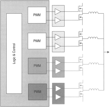
Figure 7-9 FAN5019 + FAN5009 up to four-phase controller and separate drivers.
Figure 7-10 illustrates the power management of the entire desktop motherboard. In this case our ACPI chip, FAN5063, in coordination with the rest of the chips and under ACPI control, assures smooth operation of hardware and software. This block diagram illustrates power for the following functions:
- CPU regulator VCORE
- BUS Termination VTT
- DDR Memory
- graphics chip AGP
- PCI
- clock
The illustration in Figure 7-11 reports typical currents and voltages for a modern Pentium IV class desktop PC.
Powering the Silver Box
In line with the mission of providing power from wall to board, Fairchild also provides all the electronics necessary to build the silver box, the brick inside a PC box providing the main 5 V, 3.3 V, and 12 V. The coverage goes from the bridge rectifier to the power factor correction (PFC) switcher to the PWM main switcher. The electronics in the forward path are covered, as are the opto-electronics in the feedback loop including the opto-coupler H11A817, as illustrated in Figure 7-12.
Notebook Systems
Figure 7-13 is the picture of a modern notebook mainboard (courtesy of Portelligent), while Figure 7-14 illustrates the system diagram of a modern notebook system; by comparison with the desktop system (Figure 7-5) we can see many architectural similarities between the two systems as well as some important differences like the presence of a battery as the main source of power for the notebook and the AC-DC adapter necessary for battery recharge.
Battery life is one of the most serious barriers toward the vision of “computing and connectivity anywhere anytime.” The industry needs to move from the current two hours of effective battery life to six or eight hours! This will require the optimization of every technology from battery to CPU, to display, to passives.

Figure 7-10 Motherboard power management.
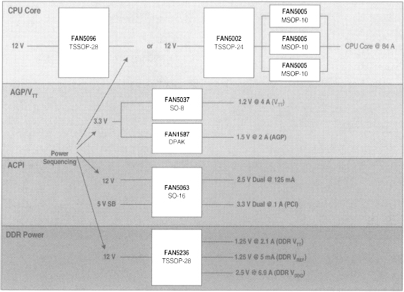
Figure 7-11 Currents and voltages for modern Pentium IV class desktop PCs.
Form factor is another important differentiator between desktop and notebook. The growing trend toward light and thin notebooks calls for thin, surface mountable components.
For these reasons, despite the initial similarities, the amount of desktop technology that can be reused in notebooks is limited.
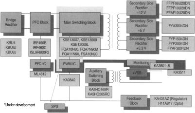
Figure 7-12 Silver box power.
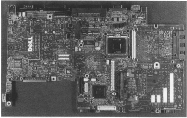
Figure 7-13 Notebook PC motherboard. (Courtesy of Portelligent)
Intel Mobile Voltage Positioning (IMVP™)
IMVP consists of a set of aggressive power management techniques aimed at maximizing the performance of a mobile CPU with the minimum expenditure of energy. Such techniques are similar to those discussed in the desktop CPU power management section but go well beyond. The additional power management techniques for notebooks are:
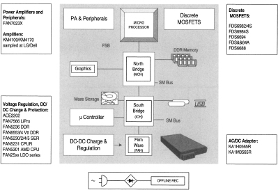
Figure 7-14 Notebook system.
Light Load Operation
At light load the switching losses become dominant over ohmic losses. For this reason, frequency of operation is scaled down at light load. This is done either automatically, commuting to light load mode below a set current threshold, or under micro control, via a digital input toggling between the two modes of operation.
Clock Speed on Demand
One of the most effective ways to contain power in notebooks is to manage the CPU clock speed and supply voltage as power dissipates with the square of the voltage and in proportion to the frequency (CV2f). Different CPU manufacturers offer variations of this technique. SpeedStep™ is Intel's recipe for mobile CPU power management while PowerNow™ is AMD's version. The bottom line is that for demanding applications, such as playing a movie from a hard disk drive, the CPU gets maximum clock speed and highest supply voltage, thereby yielding maximum power. Conversely, for light tasks like writing a memo, the power is reduced considerably.
Accordingly, when customers buy a 1.2 GHz PIV machine, they really get a CPU that may sometimes run at peak clock speed of 1.2 GHz.
Powering the Entire Mobile Motherboard
Figure 7-15 illustrates the power scheme for the entire mobile motherboard.
In this case the system runs under ACPI, as illustrated by the blocks under S3 (Suspend to RAM) and S5 (Soft Off) control, as well as under one of the mobile specific power saving schemes like Intel IMVP discussed earlier.
Figure 7-16 reports typical currents and voltages for a modern Pentium IV class notebook PC.

Figure 7-15 Powering the mobile motherboard.
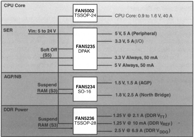
Figure 7-16 Current and voltages on the notebook motherboard.
Notebook AC-DC Adapter
Figure 7-17 shows the simplified application of a notebook AC-DC adapter based on Fairchild components, from the bridge rectifier to the offline converter (FSDH0165) to the opto loop (H11A817A opto coupler and KA431 voltage reference), which, together with the transformer T provides electric isolation between the high voltage on the AC line side and the low voltage on the load side. The control is a constant current/constant voltage (CC/CV) implementation geared toward the charging of lithium batteries. The output voltage can be easily adjusted for 3s + 2p (three series, two parallel cells pack) or 2s + 3p packs by simple scaling of a resistor divider (not shown in the figure).
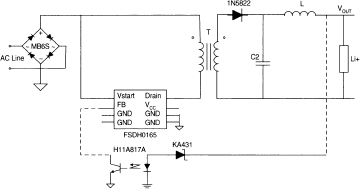
Figure 7-17 AC-DC adapter for notebook.
Future Power Trends
The pressure will not relent for the motherboard power management designer in the future. With performance and complexity increasing and shrinking form factors, the challenge will move from handling rising power to handling rising power density! The future motherboard will pack more and more power in less and less space, calling for new power technologies delivering unprecedented power densities obtainable only by a new generation of discrete MOSFETs able to work at many MHz of clock speed without appreciable losses in conjunction with all ceramic input and output bulk capacitors and smart PWM controllers capable of working reliably at very low duty cycles and high clock frequencies.
7.2 Computing and Data Communications Converge at the Point of Load
The convergence of computing and communications—“Commputing”—is happening both on the signal and the power path, creating new opportunities as well as challenges for designs. Silicon integration of computing, communications, and wireless functions on the same die, or on the same process technology, is blurring the lines between computing and communications. Powering this silicon requires a good understanding of a new environment that does not conform well to traditional schemes and classifications.
The Proliferation of Power Supplies
The two end points in the power chain are the “load” and the “wall power.” The load end of the chain is in constant evolution, resulting in continuous changes that generate new opportunities and new challenges. The technology driver on the load side is ultimately Moore's law. Doubling the number of transistors per a given area every 18 months creates a technology hierarchy by which the CPU—at the top of the food chain—is designed with the smallest minimum feature (90 nm in 2004–5) and requires the lowest supply voltages (1–1.5 V). Consequently, the previous generation fab infrastructure at 130 nm gets recycled down the food chain for the next high protein product—say memory—that gets powered at voltages around 2.5 V or lower. This cycle goes on and on. As the performance of such loads (e.g., CPUs, memories, chipsets) tends to go up while voltage decreases, the end result is an increase in power (Watts) demand.
When such a load, say a CPU, is part of a computing system, it gets powered by a voltage regulator. The voltage regulator typically is referred to as voltage regulator module if the power supply is a module plugging into a socket on the motherboard, or Voltage Regulator Down (VRD) if the same circuitry is built-in permanently “down” on the motherboard. When the same load is part of a communications system, it will be powered essentially by the same regulation electronics, now called the Point of Load regulator or simply POL.
On the wall power side we have two different power distribution systems: the 48 V power for telecom systems and the AC line (110 V or 220 V AC) for computing. Figure 7-18 illustrates and compares the two systems.
Telecom Power Distribution
Traditionally, telecom systems (Figure 7-18a) have distributed DC power (−48 V typically) obtained from a battery backup that is charged continually by a rectifier/charger from the AC line. This is the case for the power distribution in land telephones for example. Subsequently, this 48 V (in reality a voltage spreading from 36 V to 72 V) is converted into various low positive DC voltages (Figure 7-18a shows 12 V only for simplicity). This down conversion generally is accomplished by isolated DC-DC converters referred to as bricks, although non-isolated buck converters are sometimes used in telecom.
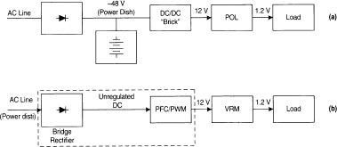
Figure 7-18 (a) Telecom versus (b) Computing power distribution system.
Isolation in bricks is driven by a number of technical factors, including cleaner ground loops, ease of handling the wide input to output voltage ratios (easily 10:1) by means of the transformer turn ratio, and inherently good over-voltage protection of the load due to the low voltage at the output of the transformer. Such a 12 V (or 5 V) bus may then be reduced down to the final voltage rails (3.3 V, 2.5 V, 1.2 V, etc.) by means of a DC-DC converter for each rail or even one for each single load, depending on the overall power management scheme. This type of low voltage DC-DC converter is referred to as point of load in telecom systems.
Computing Power Distribution
In a typical computing system (Figure 7-18b), such as a desktop PC, the power is drawn from the AC line. After rectification (AC to unregulated DC voltage conversion), the high input voltage is “bucked” down to the standard 12 V, 5 V, and 3.3 V busses by the PFC and PWM block. The silver box inside the PC box performs the down conversion. These voltages are then delivered by a cable to the motherboard, where they are reduced to the final voltage rails by VRMs, VRDs, and other types of voltage regulators.
Multiphase Buck Converter for POLs and VRMs
POLs and VRMs essentially are modules and come in a number of more-or-less standard form factors. Standardization and modularization differentiate these elements and make them specific to the application at hand, but at their heart they are powered by similar technologies and architectures. Their similarity derives from the fact that they are powering similar or identical loads from similar or identical input voltages.
The most popular architecture for step-down regulators, from 12 V or less to any voltage down to 1 V or less, is the non-isolated, multiphase interleaved buck converter.
The buck converter is a very popular and resilient architecture, thanks to its simplicity and effectiveness. Interleaved multiphase is the feature that has given a new lease on the life of this architecture. Multiphase refers to paralleling of two or more buck converters, and interleave signifies the time spacing of the clock cycles between the converters. Figure 7-19 refers to two buck converters (or two slices or phases of a multiphase buck converter) working in opposition of phase.
In Figure 7-19(a), the two clocks in phase opposition are generated at the output of a logic device (see glossary), starting from a master clock (MCK). The currents in each phase have very high DC components and a small ripple on top of such DC interleave is all about reducing that ripple amplitude even more, as the ripple represents noise or deviation from an ideal direct current waveform. Hence in this discussion we ignore the DC components and focus only on the variable content, or ripples called IΦ1RIPPLE and IΦ2RIPPLE Figure 7-19(b). In the same Figure 7-19(b), I2ΦRIPPLE the resulting ripple current after the currents in the two slices are summed. The interleave produces these fundamental benefits:
Effective operation at twice (or n times for n slices) the single slice frequency without the switching losses associated to high frequency of operation.
Smaller output ripple as demonstrated graphically in Figure 7-19(b) by the smaller amplitude of the resulting ripple compared to the amplitude of the ripple components. On the other hand, instead of working toward a smaller ripple, this architecture can be utilized to maintain a specified ripple with smaller and hence cheaper output components (inductors and capacitors).

Figure 7-19 Two-phase interleaved (a) buck converter and (b) output ripple current waveforms.
The higher duty cycle and higher on-time is demonstrated in Figure 7-19(b) by the longer duration of the positively sloped segments in the resulting ripple compared to the ripple components. Higher on-time means lower peak currents within a clock cycle. Since the on-time is the time during which current is drawn from the input capacitors, lower peak currents lead to savings in input capacitors as well.
An issue that needs attention when it comes to interleaved schemes is phase current balancing, or the need to assure that all phases carry an identical amount of current. This can be accomplished in many ways, from simple ballast schemes to active current sensing and balancing.
Conclusion
The convergence of computing and communications brings together two cultures and, in fact, two separate power universes, each with their own language, systems, and classifications. Power distribution at the source starts very differently for these two fields, but at the point of load there is clear convergence. When we dig below the surface of VRMs and POLs, we find the same technologies and architectures at play and between the latter, the interleaved buck converter rules.
7.3 Efficient Power Management ICs Tailored for DDR-SDRAM Memories
Introduction
A new type of Single Data Random Access Memory (SDRAM), Double Data Rate (DDR) DDR-SDRAM for short, has gained popularity in desktop and portable computing thanks to its superior performance (initially 266 Mbps data rate versus 133 Mbps data rate for plain SDRAM) and low power dissipation at a competitive cost when compared to competing memory technologies. Subsequently, the DDR data rate has increased to 400 Mbps. A second generation DDR, or DDR2 (JESD79-2A), has been introduced recently, extending the data rate from 400 up to 667 Mbps. DDR memories require a new and more complex power management architecture in comparison with the previous SDRAM technology.
This chapter reviews the power requirements for DDR-SDRAM memories, covering static, transient, and stand-by modes of operation. Alternative schemes of power management are discussed and an example of a complete power management system, based on efficient switching voltage regulation, is provided. Finally, future trends in power management for DDR-SDRAM memories are examined.
DDR Power Management Architecture
Figure 7-20 illustrates the basic power management architecture for first generation DDR memories.
In DDR memories the output buffer is a push-pull stage, while the input receiver is a differential stage. This requires a reference bias midpoint VREF and, consequently, an input voltage termination capable of sourcing, as well as sinking, current. This last feature (sourcing and sinking current) differentiates the DDR VTT termination from other terminations present in the PC motherboard, noticeably the termination for the Front System Bus (FSB), connecting the CPU to the Memory Channel Hub (MCH), which requires only sink capability due to termination to the positive rail. Hence, such DDR VTT termination cannot reuse or adapt previous VTT termination architectures and requires a new power design.
In first generation DDR memories the logic gates are powered by 2.5 V. Between any output buffer from the chipset and the corresponding input receiver on the memory module, typically we find a routing trace or stub, that needs to be properly terminated with resistors RT and RS as indicated in Figure 7-20. When all the impedances, including that of the output buffer are accounted for, each terminated line can sink or source ±16.2 m A. For systems with longer trace lengths between transmitter and receiver, it may be necessary to terminate the line at both ends, doubling the current.

Figure 7-20 Illustration of DDR power supply architecture.
The 2.5 V VDDQ required for the DDR logic has a tolerance of ±200 mV. To maintain noise margins, DDR termination voltage, VTT, is required to track VDDQ. It must be equal to VDDQ/2, or approximately 1.25 V, with an accuracy of plus or minus three percent. Finally, the reference voltage, VREF, must be equal to VTT to +40 mV. These tracking requirements, plus the requirement that VTT can both sink and source current, are the features that present the unique challenges of powering DDR memory.
Worst Case Current Consumption
VTT Termination
Assuming the following structure for a 128 Mbyte memory system:
- 128 bit wide bus
- 8 data strobe
- 8 mask bits
- 8 VCC bits
- 40 address lines (two copies of 20 addresses)
- 192 lines
With each line consuming 16.2 mA we have a maximum current consumption of
![]()
VDDQ Power Supply
VDDQ sources current during the phase in which VTT sinks current. It follows that the current for VDDQ is unipolar and its maximum equals VTT's maximum value of 3.11 A.
Average Power Consumption
A 128 Mbyte memory system is typically made up of 8 × 128 Mbit devices and consumes an average power of 990 mW excluding the VTT termination power.
It follows that the average current IDDQ drawn from VDDQ will be
![]()
Similarly, the average power PTT consumed by the termination resistors is 660 mW.
It follows that the current ITT drawn from VTT will be
![]()
Finally the VREF current, IREF is selected of a value high enough for the VREF supply to exhibit low enough impedance to yield good noise immunity (< 5 mA).
In summary, the main static parameters for the design of a 128 Mbyte DDR memory power management system are

Naturally if VDDQ is utilized to power other loads besides the termination load then its sizing must be increased accordingly.
Transient Operation
The governing documents for DDR memory, JEDEC, JESD79, and JESD 8-9, specify that the VTT voltage must be equal to half the VDDQ voltage with a tolerance of plus or minus three percent. This tolerance should include load transients on the bus caused by the lines transitioning. However, two items necessary for evaluation of the capacitor requirements for the VTT supply are missing from this: the JEDEC spec does not say with what bandwidth VTT must track VDDQ, nor does it specify the maximum load transient that VTT can have.
In practice, it appears that the intent of the spec was to maximize noise margins. Thus, while it is not mandatory for VTT to follow half of VDDQ at all times, the greater the bandwidth with which it does so, the more robust the system. For this reason, a wide-bandwidth switching converter is desirable for generating VTT.
For the VTT load transient, conceivably the current could step from +3.11 A down to −3.11 A, from sourcing to sinking current. This 6.22 A step with a 40 mV window would require an output capacitor with an ESR of only 7 mΩ. Two practical considerations moderate this requirement, however. The first is that actual DDR memory doesn't really draw 3.11 A. Measurement shows typical current in the range of 0.5–1 A. Secondly, the transition between sinking and sourcing current occurs very quickly, so quickly that the converter doesn't see it. To go from positive maximum current to negative maximum current would require that the bus go from all 1s to all 0s and then remain in that state for a time at least equal to the inverse of the converter bandwidth. Since this is something on the order of 10 µs, and since the bus runs at 100 MHz, it would need to stay at all 0s for a thousand cycles! In practice, then, the output capacitor for VTT need be only about 40 mΩ ESR.
Standby Operation
DDR memory supports standby operation. In this mode, the memory retains its contents, but it is not being actively addressed. Such a state may be seen, for example, in a notebook computer in standby mode. In standby the memory chips are not communicating so the VTT bus power can be turned off to save power; VDDQ, of course, must remain on in order for the memory to retain its contents.
Linear versus Switching
As noted earlier the average power dissipation of a DDR system is
![]()
for a total of
![]()
while a comparable SRAM system consumes 2040 mW.
If a linear regulator were used to terminate VTT, then the PTT power is processed with 50 percent efficiency according to the ratio VOUT/VIN = VTT/VDDQ = 0.5 This means that an additional 660 mW of power is dissipated in the VTT regulator, raising the total average power dissipation to 1650 + 660 = 2310 mW. Such a figure now exceeds the corresponding power dissipation figure for SDRAM, wiping out one of the advantages of the DDR memories, namely lower power dissipation.
As far as PDDQ goes, most of the power advantage comes from having a VDDQ of 2.5 V, as opposed to 3.3 V for conventional SDRAM. However, in a typical PC environment, the 3.3 V is provided by the silver box, while the 2.5 V is not available and needs to be created on the motherboard. Here again, unless an efficient regulation scheme is utilized to generate VDDQ, the power dissipation advantage is lost. So, it follows that switching regulation should be the preferred means of processing both PDDQ and PTT power for DDR memories.
Second Generation DDR—DDR2
With DDR2, VDDQ is reduced from 2.5 V down to 1.8 V and VTT from 1.25 V down to 0.9 V with a sink/source drive capability of ±13.4 mA. Accordingly DDR2 memories end up consuming much less than first generation DDR. For example, a DDR2-533 ends up consuming roughly half of the power consumed by a DDR-400. All the static and dynamic observations made in the previous sections for DDR also apply to DDR2. The termination scheme for DDR2 is slightly different from the one for DDR shown in Figure 7-20 and the termination resistors are on the chip, not the motherboard; however, an external VTT termination voltage is still necessary. At the much lower levels of DDR2 power consumption, linear regulators for VTT can be utilized, especially if simplicity and cost are a prevailing consideration over power consumption minimization.
FAN5236 for DDR and DDR2 Memories
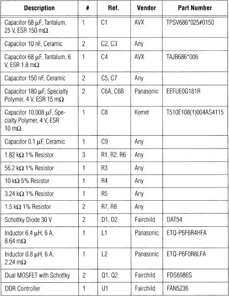
There are a variety of DDR power ICs; for example, Fairchild Semiconductor has the ML6553/4/5 with integrated MOSFETs, the FAN5066 for high power systems, and the recently released FAN5068, a combo DDR and ACPI. But the Fairchild FAN5236 (Figure 7-21) is specifically designed for all-in-one powering of DDR memory systems. Integrated in this single IC are a switcher controller for VDDQ, a switcher controller for VTT, and a linear buffer for VREF. The switcher for VDDQ runs off any voltage in the range from 5 V to 24 V. The switcher for VTT, however, is different; it is designed to run from the VDDQ power and switches synchronously with that switcher. Both switchers' outputs can range from 0.9 V to 5.5 V. Since the bus lines are driven with 2.5 V (DDR) or 1.8 V (DDR2) for VDDQ, and are terminated to 1.25 V (DDR) or 0.9 V (DDR2) for VTT, the power to some extent is circulating between VTT and VDDQ. Drawing VTT from VDDQ minimizes total circulating power, and thus circulating power losses. The VTT switcher can also be shut down for standby mode. Figure 7-21 shows the typical application and Table 7-1 the associated BOM for a 4 A continuous, 6 A peak VDDQ application. This circuit can easily be modified to set VDDQ at 1.8 V (via divider R5/R6) and VTT to 0.9 V for DDR2 applications. Appendix F provides the data sheets of FAN5236 for more technical details.
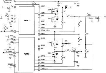
Figure 7-21 FAN5236 powering VDDQ and VTT.
Table 7-1 DDR Regulator BOM for a 4 A continuous, 6 A Peak VDDQ Application
Future Trends
As has been the trend for many years, customers will demand more and more memory to run their ever larger software applications. Systems such as the Intel boards for servers are already being designed with large amounts of DDR memory; some systems contain as much as 16 GB. DDR's decreased power requirements may still not be adequate to power such systems, hence the move toward DDR2 memory technologies. While we are just at the beginning of the DDR2 cycle, the industry is already buzzing about the next generation memory technology for PCs, DDR3 memories, which are not expected to reach the market until 2007 or later.
7.4 Power Management of Digital Set-Top Boxes
The Digital Set-Top Box (DSTB) market is one of the fastest growing applications for semiconductors. The market in millions of units is bigger and is expanding faster than the notebook market, offering tremendous opportunities for digital and analog semiconductor manufacturers. In this section, we will focus on the power management ICs that power the digital set-top box.
Set-Top Box Architecture
DSTB s control and decode compressed television signals for digital satellite systems, digital cable systems, and digital terrestrial systems. In the future, DSTBs will be an important means of access to the Internet for web browsing.
Figure 7-22 shows the main elements of a set-top box, from the video and audio processing sections to the CPU, memory, and power management sections.
Contrary to the PC architecture, which is well established and dominated by a few players, the set-top application is still going through an exciting phase of evolution and creativity. Today, there are many architectures and many implementations on the market. They range from a classic PC-like architecture based on Athlon or Pentium CPUs with associated chipsets, to embedded architectures with varying degrees of integration, all the way up to very large scale integrated circuits that include all but tuner, modem, and memory functions (see Figure 7-22).
In each case, power to each element of the architecture must be delivered readily and efficiently.
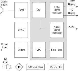
Figure 7-22 Digital set-top box block diagram.
Power Management
The strategies for powering set-top boxes are as diverse as their architectures. However, the underlying digital technologies are common to sister applications like PCs and handheld computers. Such commonalties allow the power system designer to draw from a rich portfolio of Application-Specific Standard Product (ASSP) ICs in order to power these devices, at least at the current stage of the game. As volumes increase and architectures solidify around a few leading core logic chipsets, it will become increasingly necessary to develop specific power management solutions for this market.
Here, however, we will reduce the discussion to two major cases: high performance and high power set-top boxes, which consume 50–240 W and require Power Factor Correction (PFC), and low power set-top boxes, below 50 W.
High Power Set-Top Boxes
In this section we will discuss a typical power management system for high power DSTBs. We will cover the AC-DC section first, then the DC-DC section.
AC-DC Conversion
Figure 7-23 shows the entire conversion chain, from wall power to an intermediate DC-DC voltage (VOUT) low enough to be safely distributed on the box motherboard. The AC line is rectified first, and then power factor corrected, and converted down to a manageable voltage VOUT (12–28 V DC) for distribution.
The rectification is accomplished with a full bridge diode rectifier and converts the alternate line voltage into a continuous—but still poorly regulated—intermediate voltage. As best efficiency is obtained when voltage and current drawn from the line are “in phase”, a PFC block forces the correct phasing by modulating the drawn current according to the shape of the input voltage. The switch Q1 (MOSFET) and the diode D1, controlled by half of FAN4803 in Figure 7-23, constitute the PFC section. The top portion of Figure 7-24 shows the PFC control loop with the multiplier block accomplishing the phase modulation. Finally this power-factor corrected voltage is converted down to a low voltage that is usable by the electronics on the motherboard by means of a “forward” converter (switches Q2 and Q3, diodes D1–D5, and the second half of FAN4803 in Figure 7-23). This last conversion requires electrical isolation between the high input and the low output voltages. This is accomplished via the utilization of a transformer (T) in the forward conversion path and an opto-coupler in the feedback path.

Figure 7-23 AC-DC power Conversion with PFC.
DC-DC Conversion
With an appropriate DC voltage (12–24 V) delivered by the offline section, all the low voltage electronics on the motherboard can be safely powered. In Figure 7-24 the entire distribution of DC power on the motherboard is shown.
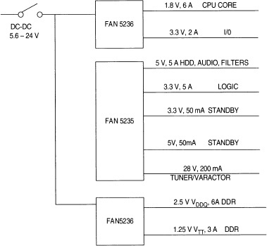
Figure 7-24 DC-DC regulation system for high power DSTB.
A total of nine different power lines are serviced, namely the nine output lines in Figure 7-24.
These power lines are described in more detail in the following text.
A dual PWM regulator, FAN5236, shown in Figure 7-25, powers the CPU core and I/O: these two regulators have adjustable voltages down to 0.9 V. This allows them to be easily set to power multiple generations of CPUs, from 0.18 µm lithography requiring 1.8 V, to 0.13 µm requiring 1.2 V, to future 0.1 µm lithography requiring sub band-gap voltage rails.
A highly integrated PWM controller (FAN5235) produces another five of the nine voltages: two buck regulators (3.3 and 5 V), one boost regulator (28 V) and two low power/low dropout regulators for standby operation. Figure 7-26 shows the typical application of this PWM controller.
A second dual PWM regulator provides DDR memory power VDDQ (2.5 V, 6 A) and termination VTT (VDDQ/2 = 1.25 V, 3 A). The associated application diagram is similar to the one in Figure 7-25 so it is not repeated here.
Finally, Figure 7-27 shows a simplified internal functional diagram for one of the two PWM control loops of FAN5236. This controller is designed for very high efficiency: notice how the current sense (ISEN line) is done across the low side MOSFET RDSON (drain to source “on” resistance of the MOSFET), avoiding the losses and the cost of a high power current sense resistor. Notice also the dual mode control loop, PWM for constant frequency operation at high currents, and Hysteretic (a technique leading to low frequency operation at light load, with constant ripple and low switching losses) for high efficiency at light load.
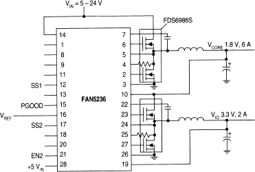
Figure 7-25 DC-DC regulation for CPU, I/O with FAN5236.
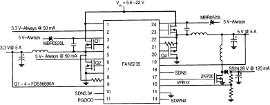
Figure 7-26 DC-DC regulation of five rails with FAN5235.

Figure 7-27 FAN5236 simplified diagram of one channel.
Low Power Set-Top Boxes
In this section we discuss a typical power management system for low power DSTB.
AC-DC Conversion
Below 50 W the architecture of the offline section becomes considerably more simple. The low level of power generally implies less sophisticated systems, for example those that lack HDDs and have less memory on board. Here the PFC section is no longer needed, and the lower power rating allows a simpler architecture. As shown in Figure 7-28, a diode bridge rectifier, in conjunction with a simple fly-back controller (KA5x03xx family) with a minimum number of external components, handles the entire offline section. The isolation requirements as per the high power offline discussed in the high power AC-DC conversion section still apply here.
The multi-chip approach to integration of the controller family allows such simplification (Figure 7-29). The SO8 package houses two dies, a controller die and a high voltage MOSFET die on board. Here again power-hungry discrete current sense resistors are avoided, in this case by means of a ratioed sense-fet technique on board the discrete element.

Figure 7-28 Low power AC-DC conversion.
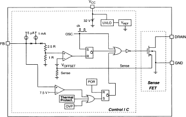
Figure 7-29 offline controller KA5H0365 simplified block diagram.
DC-DC Conversion
Here the same type of controllers utilized in the previous section can be employed, although with smaller external discrete transistors and passive components, which leads to a much more compact set-top box. Figure 7-30 shows a system that needs only two controllers to power the entire DC-DC on the motherboard.
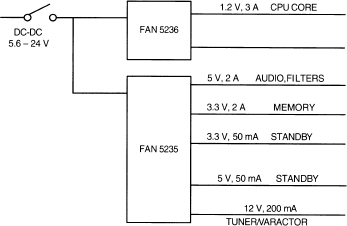
Figure 7-30 DC-DC regulation for low power systems.
Conclusion
We have discussed the power management needs of set-top boxes, covering two cases at opposite ends of the power spectrum.
The current generation of set-top boxes can be powered by a slew of ASSPs developed for the PC and handheld markets. As volumes increase and architectures solidify around a few leading core logic chipsets, dedicated ASSP ICs for set-top boxes will become necessary to allow increased performance at competitive cost.
7.5 Power Conversion for the Data Communications Market
This section discusses the transition from traditionally voice-centric telephony to converged voice and data over Internet Protocol (IP) and its implications for the power conversion of such systems. A few power conversion examples are provided complete with application schematics.
Introduction
The arm wrestling between voice and data has concluded in favor of the latter, with all the major data communications players now posturing for leadership of the migration from traditional voice to IP telephony. In the short term, the huge investments locked in the traditional telephony infra-structure and the new investments in data over IP necessitate that over the next few years we will have to provide power conversion for both types of systems as well as for the converged systems to come.
Current Environment with Separate Networks
Figure 7-31 shows the current telephony situation. Voice travels from traditional Private Branch Office (PBX) to Central Office, Switch, and finally to the Public Switch Telephone Network (PSTN). The data travels from routers to Wide Area Networks (WAN), and the video goes through a third independent path.

Figure 7-31 Separate networks for voice, data, and video.
Migration to Converged Voice/Data/Video IP
Figure 7-32 shows the envisioned converged Voice/Data/Video system over IP. At the center of this new universe is the Internet Protocol Wide Area Network, with all the services, including voice, data, video, and wireless communications gravitating around it.
Telecom −48 V DC Power Distribution
Usually telecom systems distribute a DC power (−48 V typically) obtained from a battery backup that is charged continually by a rectifier/charger from the AC line. Subsequently the −48 V is converted into various low positive DC voltages (Figure 7-33 shows 12 V only for simplicity) as well as back to AC voltages as necessary.
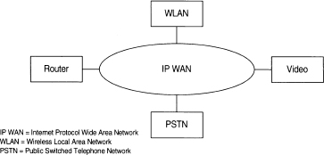
Figure 7-32 Voice/Data/Video over IP.

Figure 7-33 Telecom −48 V DC power distribution.
Datacom AC Power Distribution
Data centric systems tend to rely on an Uninterruptible Power Supply (AC UPS) front end for distributing AC power, which subsequently is converted into the basic constituents: −48 V, AC power, and low voltage DC (again, for simplicity Figure 7-34 only shows a 12 V DC).
With the advent of the converged systems, the telecom versus datacom separate approaches to power distribution will converge into new architectures. However, the bottom line is that at the board or backplane level the usual voltages will need to be delivered, namely 12 V and 5 V, as well as 0.9 V, 1.8 V, 2.5 V, and 3.3 V, with more to come.
The delivery of such low voltages starting from DC or AC power will be the focus of this document from here on.

Figure 7-34 Datacom AC power distribution.
DC-DC Conversion
Figure 7-35 shows the −48 V to +VOUT (+5 V, +12 V etc.) with a forward converter architecture based on the ML4823 high frequency PWM controller.
Figure 7-36 shows the DC-DC conversion from 12 V and 5 V down to a variety of typical low voltages required by modern electronic loads.
The conversion down to heavy loads is done with synchronous rectification switching regulators of single or multiphase interleaved type, while for lighter loads linear regulators can be utilized.
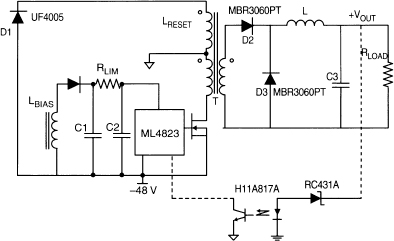
Figure 7-35 −48 V to +VOUT conversion.
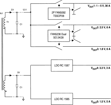
Figure 7-36 DC-DC conversion diagram.
FAN5092 Two-Phase Interleaved Buck Converter
The FAN5092 step-down (buck) converter (Figure 7-37) is ideal for data communications applications. This IC is a two-phase interleaved buck converter switching up to 1 MHz per phase. The application diagram illustrates conversion from 12 V down to 3.3 V in a 12 V-only input voltage source environment. The chip integrates the controller and the drivers on a single die. The high frequency of operation is enabled by:
- the monolithic approach of integrating controller and drivers on board
- a fast proprietary leading edge valley control architecture with 100 nanoseconds of response time
- the strongest drivers in the industry at 1 Ω of source and sink impedance for both high and low side driver of each phase
Such combination of features, together with loss-less current sensing via RDSON sense allows for a very efficient delivery of power with very small passive components, leading to record levels of power density.

Figure 7-37 FAN5092 application circuit.
The application diagram of the IC is shown in Figure 7-37 for a 3.3 V, 30 A load. Optimum companions of the FAN5092 are the Fairchild discrete DMOS FDB6035AL for high side pass transistors Q1,2 and FDB6676S for low side synchronous rectification transistors Q2,4.
Two FAN5092 converters can be paralleled by means of doubling the above application and connecting together two pins (pin 26 and pin 15). This will allow handling of loads up to 120 A.
FAN5236 Dual Synchronous Buck Converter
The FAN5236 PWM controller (Figure 7-38) provides high efficiency and regulation for two output voltages adjustable in the range from 0.9 V to 5.5 V. Synchronous rectification and hysteretic operation at light loads contribute to a high efficiency over a wide range of loads. The hysteretic mode of operation can be disabled separately on each PWM converter if PWM mode is desired for all load levels. Again high efficiency is obtained by using MOSFET's RDSON for current sensing. Out-of-phase operation with 180 degree phase shift reduces input current ripple.
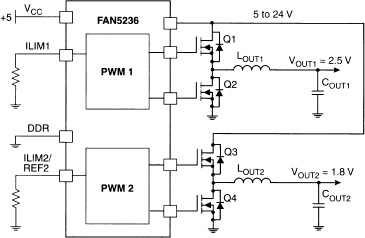
Figure 7-38 FAN5236 block diagram.
RC1585/7 Linear Regulators
In some cases, it makes sense to use linear regulators if the input to output voltage difference is sensibly less than the output voltage. Figure 7-36 showcases Fairchild's RC1587, 3 A and RC1585, 5 A linear regulators.
For more details and a complete bill of materials please refer to the FAN5092, FAN5236, RC1585, RC1587, and FOD2712 data sheets available on the Fairchild website www.fairchildsemi.com.
For KA5H0365, please refer to the data sheet as well as to Fairchild Power Switch (FPS) Application Notes for Switch Mode Power Supply (SMPS) design, also available on the Fairchild website.
Conclusion
The merging of data, voice, and video blurs the line between computing and communications. The smart loads of either application draw from the same advanced, high-density, sub-micron, low voltage CMOS technologies and require similar solutions for distributed power conversion. Fair-child expertise in power conversion for computing and communications offers proven solutions to the merging converged data communications market.