
12Sensitive Materials and Image Sensors
Many light-sensitive substances, varying widely in their sensitivity, are known. Conventional photographic materials use silver halides, which are light-sensitive compounds formed by the combination of silver with members of the halogen group of the elements (bromine, chlorine and iodine).
Photographic materials are coated with suspensions of minute crystals (with diameters from 0.03 μm for high-resolution film to 1.5 μm for a fast medical X-ray film) of silver halide in a binding agent, nowadays almost invariably gelatin. These photographic suspensions are called emulsions, although they are not emulsions but solid suspensions. The crystals are commonly termed grains. In materials designed for the production of negatives, the halide is usually silver bromide, in which small quantities of iodide are also normally present. With papers and other positive materials the halide may be silver bromide or silver chloride or a mixture of the two. The use of two silver halides in one emulsion results not in two kinds of crystal but in crystals in which both halides are present, although not necessarily in the same proportion in all crystals. Photographic materials containing both silver bromide and silver iodide are referred to as iodobromide materials, and those containing both silver chloride and silver bromide as chlorobromide materials.
Silver halides are particularly useful in photography because they are developable, which means that the effect of light in producing an image can be amplified with gain in sensitivity of about one thousand million times. The image produced when photographic materials are exposed to light is normally invisible and termed the latent image.
Electronic image sensors, currently, rely almost exclusively on charge-coupled devices (CCDs), although complementary metal oxide semiconductor (CMOS) image sensors are also used. These use regular arrays of light-sensitive elements (picture elements or pixels). The CCD has the ability to convert light intensities into voltage signals. It has the three basic functions of charge: collection, transfer and conversion into a measurable voltage. The basic element of the CCD is the metal oxide semiconductor (MOS) capacitor, which is also called a gate. Changing the voltage at set time intervals applied to the gate allows the charge to be stored or transferred. Charges are transferred from gate to gate until they reach the sensing node where they are measured, amplified and ultimately digitized in a such a way that their spatial and temporal positions are known. CCDs were invented thirty years ago by W.S. Boyle and G.E. Smith of Bell Laboratories in the USA and were first applied in video cameras. In the early 1980s Sony produced a prototype electronic camera system for still image recording and CCD based electronic cameras are becoming increasingly popular as their resolution increases and their cost decreases.
Latent Image Formation in Silver Halides
The latent image is any exposure-induced change occurring within a silver halide crystal that increases the probability of development from a very low value to a very high value. Although all crystals will eventually be reduced to metallic silver if developed for a sufficient time, the rate of reduction is very much greater for those crystals that bear a latent image. It is generally believed that this change is the addition at a site or sites on or within the crystal of an aggregate of silver atoms. The latent image sites are probably imperfections and impurities (e.g. silver sulphide specks) existing on the surface and within the bulk of the silver halide crystal. Light quanta are absorbed, releasing photoelectrons which combine with interstitial silver ions to produce the atoms of silver. Interstitial silver ions are mobile ions displaced from their normal positions in the silver halide lattice and are present in silver halide crystals of an emulsion prior to exposure. The general reaction can be represented by the equations:
![]()
where hυ is a light quantum, e− is the electron and the dots represent electrons associated with atoms.
The energy levels relevant to latent image formation are shown schematically for a silver bromide crystal in Figure 12.1. Discounting thermal fluctuations, absorption of a quantum of energy greater than 2.5 eV (electron volts) is necessary in order that an electron may be raised from the valence to the conduction band. The valence band is essentially that filled band of energy in which the electrons exist. The conduction band is that empty group of energy levels, if electrons are excited to this band they are free to move and conduction can take place. Between these two levels is the band gap in which electrons cannot exist. An energy of 2.5 eV is equivalent to a wavelength of approximately 495 nm, and corresponds to the longest wavelength of the spectral sensitivity band of ordinary silver bromide. Also indicated in Figure 12.1 are the relevant energy levels of an adsorbed dye molecule suitable for sensitizing silver bromide to longer wavelengths. It can be seen that a photon of energy much less than 2.5 eV may, upon absorption by the dye, promote the molecule from its ground energy state to its first excited state. If the excited electron can pass from the dye to the crystal, latent image formation may proceed. In this way it is possible to sensitize silver halides to green and red light and even infrared radiation, although it should be noted that in the last case electron transitions arising from the thermal effects may cause crystals to become developable without exposure. Excessive fogging can result and careful storage and usage of such materials is necessary.

Figure 12.1Schematic representation of the energy levels relevant in latent image formation
Although a number of different mechanisms have been suggested to account for the details of latent image formation, there is considerable experimental evidence supporting the basic principle suggested by Gurney and Mott in 1938. The essential feature of this treatment is that the latent image is formed as a result of the alternate arrival of photoelectrons and interstitial silver ions at particular sites in the crystal. Figure 12.2 shows the important steps. Here the process is considered as occurring in two stages:
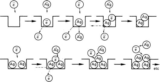
Figure 12.2Latent image nucleation (top row). Initial growth (bottom row)
- The nucleation of stable but sub-developable specks.
- Their subsequent growth to just-developable size and beyond.
The broken arrows indicate the decay of unstable species, an important characteristic of the process. The first stable species in the chain is the two-atom centre, although it is generally accepted that the size of a just developable speck is 3 to 4 atoms. This implies that a crystal must absorb at least 3 to 4 quanta in order to become developable, but throughout the sequence there are various opportunities for inefficiency, and as a general rule far more than this number will be required. During most of the nucleation stage the species are able to decay, and liberated electrons can recombine with halogen atoms formed during exposure. If this occurs, the photographic effect is lost. The halogen atoms may also attack the photolytically formed silver atoms and re-form halide ions and silver ions. Although gelatin is a halogen acceptor and should remove the species before such reactions can occur, its capacity is limited and its efficiency drops with increasing exposure.
These considerations lead to possible explanations for low-intensity and high-intensity reciprocity-law failure. During low-intensity exposures, photo-electrons are produced at a low rate and the nucleation stage is prolonged. As a result the probability of decay and recombination is relatively high. During high-intensity exposures large numbers of electrons and bromine atoms are simultaneously present in the crystals. Such conditions can be expected to yield high recombination losses. Also, nucleation may occur at many sites in a single crystal, producing large numbers of very small silver specks.
Image Formation by Charge-Coupled Devices
The heart of the CCD and most electronic image sensors is the metal oxide semiconductor (MOS), which is illustrated in Figure 12.3. It comprises silicon doped with impurities, such as aluminium, so that an acceptor level of positive holes is formed in the band gap, which is able to accept electrons excited from the valence band. Since silicon has a band gap of 1.1 eV it has a sensitivity up to about 1100 nm. Whilst this may be an advantage for recording in to the IR region of the spectrum in certain applications, it is a disadvantage for imaging within the visible region of the spectrum and would result in incorrect tone and colour reproduction. CCD cameras have a special IR absorbing filter included to restrict their spectral response to the visible region.

Figure 12.3Energy levels in a p-type semiconductor
Figure 12.4 is a simple schematic diagram of p-type silicon MOS capacitor. The positive voltage to the gate (Vgate) causes mobile positive holes to migrate to the ground electrode. The region with an absence of positive charge is called the depletion region. If light of sufficient energy (greater than 1.1 eV) is absorbed in the depletion region an electron-hole pair is produced. The electron remains in the depletion region (see Figure 12.4) whilst the positive holes migrate to the ground electrode. The number of electrons that can be retained in the depletion region is the well capacity, which depends upon the physical sizes of the oxide layer and the gate electrode area as well as the applied voltage.

Figure 12.4The basic element of an electronic image sensor: p-type silicon metal oxide semiconductor
In order to record images the sensor contains a large number of elements (pixels) in the form of a two-dimensional array for most CCD based cameras and a linear array for many scanning devices and some types of studio based cameras. The sensor size, number of picture elements and the number of grey levels are all becoming larger as the technology matures. At the time of writing, full frame (36 ´ 24 mm) 35 mm camera format size sensors are becoming available with 6 million pixels, although at relatively high cost.
The CCD array consists of a series of gates. Adjustments of the gate voltages allows transfer of electrons from well to well. This is a function of time. Figure 12.5 shows the way in which charges are transferred between neighbouring wells (1). After exposure to light, the charge in well 1 is shown in (2). If a voltage is applied to gate 2, electrons flow from well 1 to well 2 (3), and (4) shows the situation when equilibrium is reached. If the voltage to gate 1 is reduced electrons begin to be completely transferred to well 2 (5), and in (6) complete transfer is shown.
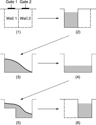
Figure 12.5Transfer of charge between neighbouring pixels in a CCD sensor (after Holst). The potential in the well increases towards the bottom of the well
Thus the charges forming the image are transferred in a time-dependent way if one considers a complete array of image elements and their gates. The clocking sequence for a three-phase device is shown in Figure 12.6. In the diagram it can be seen that only one-third of the pixel area is available (a fill factor of 33 per cent) as the well capacity (three gates).
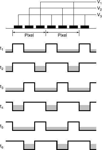
Figure 12.6Clocking sequence for a typical CCD three-phase device (after Holst). The black areas represent the gates and the shaded areas the stored charges. Different times are given by t1 etc.
There are a number of different ways in which CCDs can be configured for different readout modes. Some different array architectures are given in Figure 12.7 and include linear arrays, full-frame transfer, interline transfer and frame interline transfer. These are provided for various applications. For example, linear arrays are used in scanners and some studio based still cameras; full-frame transfers are used mainly for scientific applications; interline transfer and frame transfer arrays tend to be used in professional television systems and consumer products.
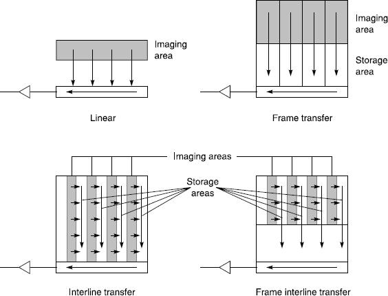
Figure 12.7CCD architectures in which the arrows indicate the movement of charge and the readout output register is shown as the horizontal box at the bottom of each diagram
The storage and transfer areas are shielded from the light. From Figure 12.7 it can be seen that the full frame transfer architecture consists of two almost identical arrays, one for imaging and one for storage, which makes them costly to produce. Interline transfer arrays, however, have shielded strips which decreases the light sensor size and may occupy only 20 per cent of the array, i.e. have a low fill factor. Like many commercial products, CCD detectors are a compromise between cost, efficiency and suitability for purpose. For example, interline transfer arrays have low fill factors but the transfer of charge is rapid. Manufacturers improve the fill factors of these devices by the inclusion of microlens arrays over the CCD, which increase the effective size of the sensor element.
So far we have only considered arrays that respond to light intensity and in order for CCD based devices to record colour three methods are used. One is to successively record each image through red, green and blue filters to additively record colour (see Chapter 14). This method is used for scanning colour originals and in some studio cameras where only static subjects are being recorded. The second method, which is commonly used in digital cameras, is to place a colour filter array (CFA) over the CCD. Although many filter arrays are used in digital cameras, a typical Bayer colour filter array is illustrated in Figure 12.8.

Figure 12.8The Bayer colour filter array (CFA)
The third method involves the use of a beam-splitter behind the lens which divides the input into three separate channels which separately record the red, green and blue signals (or other appropriate combinations) on three filtered CCD detectors. Whilst this is an expensive solution to the recording of colour it allows higher resolution than is possible with CFAs. With CFAs a single CCD is used which reduces the effective resolution and data has to be interpolated to provide the missing information. If a red area is being recorded, it can be seen from Figure 12.8 that there will be pixels which will not have been activated and the missing data has to be added.
CCDs are very complicated and sophisticated detectors and possess a number of characteristics by which they can be judged and compared. Some fundamental characteristics of CCDs are summarized in Table 12.1.
Table 12.1 Performance characteristics of CCD sensors
Characteristic |
Comment |
Detector size |
dimensions of sensor area (mm ´ mm) |
Pixel size |
physical dimensions of pixels expressed as μm × μm for each pixel, or as numbers of vertical and horizontal pixels for whole sensor area |
Fill factor |
fraction of pixel area which is sensitive to light (%) |
Full well capacity |
maximum charge (or signal) which the sensor element can hold (J/cm2, or number of electrons) |
Noise |
many sources: shot noise accompanies generation of photoelectrons and dark current electrons; pattern noise due to pixel to pixel variations; reset noise when reading the charge and added to by the amplifier; quantization noise arising from analogue to digital conversions. Expressed as rms electrons or rms volts |
Dark current |
due to thermal generation of current (number of electrons or nA/cm2) |
Dynamic range |
ratio of full well capacity to noise (dB) |
Scanning mode |
interlaced or progressive |
Resolution |
relates to detector size, pixel size and fill factor (see Chapter 24) expressed as lines/mm, dpi, cycles/mm. Often expressed as numbers of pixels or file size. Applies to the imaging system output |
Quantum efficiency |
ratio of number of electron-hole pairs produced to number of photons absorbed (maximum value unity) |
Spectral response |
plots of quantum efficiency against wavelength |
Architecture |
structure and readout modes of detector arrays |
Production of Light-Sensitive Materials and Sensors
The principal materials used in the preparation of a photographic emulsion which is coated on a base to form the sensitive layer are silver nitrate, alkali-metal halides and gelatin, and all these must satisfy stringent purity tests. The gelatin must be carefully chosen, since it is a complex mixture of substances obtained from the hides and bones of animals, and, although silver salts form the light-sensitive material, gelatin plays a very important part both physically and chemically.
Gelatin is a protein derived from collagen, the major protein component of the skin and bones of animals. It is a lyophilic or hydrophilic colloid made up of long chain molecules which are soluble in water. It possesses a number of unique properties that make it particularly suitable as a binder for silver halide microcrystals. The combination of many different physical and chemical properties in one type of chemical compound explains why it has not so far been possible to replace gelatin by a synthetic polymer as a binder for silver halides. Certain synthetic polymers may be used in conjunction with gelatin as gelatin extenders but not as a substitute. Gelatin has remarkable properties as a binding agent which are summarized as follows.
- Dispersed with water, it forms a convenient medium in which solutions of silver nitrate and alkali halides can be brought together to form crystals of insoluble silver halides. These crystals remain suspended in the gelatin in a fine state of division, i.e. it acts as a protective colloid.
- Warmed in water, it forms a solution which will flow, and, by cooling an aqueous solution of gelatin it sets to a firm gel. Thus it is possible to cause an emulsion to set firmly almost immediately after it has been coated on the base, aided by cooling. The water is removed in a current of warm air to form a coated layer that is reasonably strong and resistant to abrasion.
- When wetted, gelatin swells and allows processing solutions to penetrate.
- Gelatin is an active binding agent, containing traces of sodium thiosulphate sensitizers and nucleic acid degradation products (restrainers) that influence the speed of emulsions.
- It acts as a halogen acceptor, as described earlier.
- The properties of gelatin can be modified, by chemical reactions such as hardening or cross-linking of the gelatin chains, to make it tougher, and reduce its tendency to swell.
- It enables developer solutions to distinguish between exposed and unexposed silver halide crystals. In the absence of gelatin, silver halides are reduced to metallic silver by a developer solution regardless of whether they bear a latent image.
- Gelatin confers stability on the latent image.
Gelatins vary greatly in their photographic properties. The ‘blending’ of gelatins originating from different sources helps in producing a binder with the required properties and in obtaining consistency. Modern photographic emulsion technology tends to use ‘inert’ gelatin, i.e. gelatin containing less than five parts per million of sulphur sensitizers and nucleic-acid-type restrainers. A more recent development by gelatin manufacturers is to provide gelatins which are substantially free of all sensitizers and restrainers (‘empty’ gelatin). These gelatins may then be doped to the required degree by the addition of very small amounts of the appropriate chemicals by the emulsion manufacturer.
The essential steps involved in the preparation of photographic emulsions consist of the following:
- Solutions of silver nitrate and soluble halides are mixed in the presence of gelatin under carefully controlled conditions, where they react to form silver halide and a soluble nitrate. This stage is called emulsification.
- This emulsion is subjected to a heat treatment in the presence of the gelatin in a solution in which the silver halide is slightly soluble. During this stage the crystals of silver halide grow to the size and distribution which will determine the characteristics of the final material, particularly in terms of speed, contrast and graininess. This stage is known as the first (physical or Ostwald) ripening.
- The emulsion is then washed to remove the byproducts of emulsification. In the earliest method of doing this the emulsion was chilled and set to a jelly, shredded or cut to a small size and then washed in water. In modern practice, washing is achieved by causing the emulsion to settle to the bottom of the vessel by the addition of a coagulant to the warm solution. The liquid can then be removed by decanting etc.
- The emulsion is subjected to a second heat treatment in the presence of a sulphur sensitizer. No grain growth occurs (or should occur) during this stage, but sensitivity specks of silver sulphide are formed on the grain surface and maximum sensitivity (speed) is reached. This stage is known as the second ripening, digestion or chemical sensitization.
- Sensitizing dyes, stabilizing reagents, hardeners, wetting agents, etc., are now added.
All these operations are capable of wide variation and it is in the modification of these steps that much progress has been made in recent years, so that emulsions of extremely diverse characteristics have been produced. In a given photographic emulsion the silver halide crystals vary both in size and in the distribution of their sizes. They are said to be polydisperse unless special conditions are used in their preparation such that they are all of the same size (monodisperse). Not only does the crystal size and distribution of crystal sizes affect the photographic emulsion, but the shape of the crystals, the nature of the halides used, their relative amounts and even the distribution of the halides within a single crystal have pronounced effects.
Manufacturers of sensitive materials are able to control all these and many other factors, and to tailor-make emulsions so that the material is optimized with respect to speed and granularity for a specific application, as well as having the appropriate characteristics of tone and colour reproduction. In the past ten years much of the research and development work has led to the manufacture of colour negative films and papers of high sensitivity, low granularity and high image quality. For optimizing the sensitivity, resolution and granularity of colour negative films the individual manufacturers adopt their own individual methods.
Some examples of the various sophisticated ways of employing specific types of silver halide crystal in colour negative films are illustrated in Figure 12.9.

Figure 12.9Examples of types of emulsion grains (crystals). (a) Twin grains (Agfa). (b) Double structure (Fuji). (c) Tabular or T-grains (Kodak). (d) Cubic (Konica)
T-grains (flat tabular crystals) allow maximum sensitizing dye to be adsorbed to the grain surface, and encourage very efficient absorption of light, as well as possessing other useful optical and chemical properties that give higher resolution and lower graininess than might be expected from crystals of large surface area. Double-structure crystals optimize both absorption of light and graininess. Monodisperse crystals of appropriate size minimize light scatter within the layer, and so improve image resolution. Much of this sophisticated emulsion technology, originally devised for colour materials, has also been applied to the modern generation of black-and-white materials. Examples include Ilford’s XP-2, a monochrome film that yields a dye image and is processed in colour-processing chemicals, Kodak’s ‘T max’ films using Kodak’s ‘T-grain’ technology, and Fuji’s Neopan films which use their ‘high-efficiency’ light-absorption grain technology.
The Support
The finished emulsion is coated on to a support, usually referred to as the base, most commonly film or paper. The base used in the manufacture of films is usually a cellulose ester, commonly triacetate or acetate-butyrate, although manufacturers also use newer synthetic polymers which offer important advantages in properties, particularly dimensional stability. This makes them of special value in the fields of graphic arts and aerial survey. The first of these newer materials to be used widely was polystyrene; but the most outstanding dimensionally stable base material to date is polyethyleneterepthalate, a polyester and the raw material of Terylene fabric. As a film, polyethylene terephthalate has exceptionally high strength, much less sensitivity to moisture than cellulose-derivative films, and an unusually small variation in size with temperature (see Table 12.2). Being insoluble in all common solvents, it cannot be fabricated by the traditional method of ‘casting’ (spreading a thick solution of the film-former on a moving polished band or drum, evaporating off the solvent and stripping off the dry skin). Instead, the melted resin is extruded, i.e. forced through a die, to form a ribbon which is then stretched while heated to several times its initial length and width. A heat-setting treatment locks the structure in the stretched condition, and the film is then stable throughout the range of temperatures encountered by photographic film. Polystyrene is extruded in a somewhat similar manner.
Table 12.2 Properties of supports
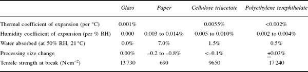
Film base differs in thickness according to the particular product and type of base, most bases in general use coming within the range of 0.08 mm to 0.25 mm. Roll films are generally coated on 0.08 mm base, miniature films on 0.13 mm base, and sheet films on 0.10 mm to 0.25 mm base. Polyethylene terephthalate base can usually be somewhat thinner than the corresponding cellulosic base because of its higher strength.
Glass plates have now almost entirely been replaced by films but they are still used occasionally in a few specialized branches such as astronomy, holography and spectroscopy, because of their dimensional stability and rigidity, although the dimensional stability of modern safety film bases and the application of electronic sensors is such that the use of glass plates is now rarely essential. An additional advantage of using plates is that they lay flat in the camera; however, these advantages are outweighed by their disadvantages of high cost, fragility, weight, storage space requirements and loading difficulties.
The paper used for the base of photographic and digital hard copy must be particularly pure. Photographic base paper is, therefore, manufactured at special mills where the greatest care is taken to ensure its purity. Before photographic paper is coated with emulsion, the base is usually coated with a paste of gelatin and a white pigment known as baryta (barium sulphate), to provide a pure white foundation for the emulsion, giving maximum reflection. However, most modern paper bases are not coated with baryta but are coated on both sides with a layer of polyethylene and are known as PE or RC – polyethylene or resin-coated papers respectively (Figure 12.10). The upper polyethylene layer contains titanium dioxide as the white pigment and optical whiteners. They are impermeable to water, which prevents the paper base from absorbing water and processing chemicals. This results in substantially shorter washing and drying times than are required by traditional baryta-coated fibre-based papers.

Figure 12.10Construction of photographic papers. (a) Baryta paper. (b) Polyethylene or resin-coated paper
Different papers are required for the hard copy output of digital images, particularly if ‘photographic quality’ is a requirement. In addition to the use of heavyweight bases of 264 g/m2, papers for ink-jet printing require special surface coatings which guarantee homogeneous surface penetration, minimum image spread, high gloss and brightness. Coated paper surfaces may use relatively thick coatings (20 μm) of silica in a starch binder. Dye diffusion thermal transfer (D2T2) papers also have special surface coatings to optimize dye uptake, stability, gloss and brightness and the ability to withstand the high temperatures required for the dye transfer.
Coating the Photographic Emulsion
The coating of modern materials is a complex task and the coating methods in current use are the subject of commercial secrecy. One of the earliest forms of coating flexible supports was ‘dip’ or ‘trough’ coating (see Figure 12.11), but this method has been replaced by one or other of the coating techniques outlined below. Dip coating is a slow method because the faster coating results in thicker emulsion layers which are difficult to dry, and may have undesirable photographic properties.
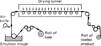
Figure 12.11Schematic diagram of a coating machine
In order to increase the coating speed this method has been modified by the use of an air-knife, which is an accurately machined slot directing a flow of air downwards onto the coated layer and increases the amount of emulsion running back into the coating trough. Coating by this method results in the use of more concentrated emulsions, faster coating speed and thinner coated layers. Other more modern coating methods employ accurately machined slots through which emulsion is pumped directly onto the support (slot applicator or extrusions coating) or after flowing down a slab or over a weir onto the support (cascade coating) (Figure 12.12). Such coating methods allow coating speeds to be far higher than were possible with the more traditional methods. This allows very high coating speeds to coat base material approximately 1.4 metres wide. Modern monochrome materials have more than one layer coated; colour materials may have as many as fourteen layers, while instant self-developing colour-print films have an even more complex structure. In modern coating technology, many layers are coated in a single pass of the base through the coating machine, either by using multiple slots or by using a number of coating stations, or by a combination of both. The coated material is chilled to set the emulsion, after which (with films and papers) a protective layer, termed a non-stress superheat, is applied to reduce the effects of abrasion. The emulsion is then dried.

Figure 12.12Cross-section of a multiple cascade coating head (Agfa)
With fast negative materials it is usually impossible to obtain the desired properties in any single emulsion. Two emulsions may then be prepared which together exhibit the desired characteristics. These may be mixed and coated as a single emulsion, or they may be applied as two separate layers, an undercoat and a top coat. For the highest speeds the top coat consists of the fastest component emulsion while the undercoat comprises a slower layer. This arrangement gives the required combination of speed, contrast and exposure latitude.
Charge-Coupled Devices (CCDs)
Photographic sensors are complex to manufacture and require a number of stages and components of high purity. They can be produced in large lengths and widths to provide homogeneous sensors of large area which are subsequently cut to appropriate sizes. CCD sensors, however, are far more difficult to produce and are batch multi-stage processes based on MOS techniques. Their fabrication involves deposition of many layers of silicon compounds, implantation of specific ions and a metallization layer on ultra-pure silicon wafers. Theuwissen (1996) gives details of 29 stages involved in the production of a typical CCD sensor. This explains their relatively high cost and difficulty in mass producing a 24 × 36 mm, or larger, full frame imager because of the increase in defects as the sensor size increases and the high wastage rate.
Sizes and Formats of Photographic and Electronic Sensors and Media
Sheet films and papers are supplied in a great many sizes. The nominal sizes in most common use are given in Table 12.3.
Table 12.3 Some common sizes of sheet film and papers
Size (cm) |
Size (inches) |
10.2 × 12.7 |
4 × 5 |
10.5 × 14.8 (A6) |
4 × 5.5 |
14.8 × 21.0 (A5) |
5.8 × 8.3 |
16.5 × 21.6 |
6.5 × 8.5 |
20.3 × 25.0 |
8 × 10 |
21.0 × 29.7 (A4) |
8 × 11.5 |
25.4 × 30.5 |
10 × 12 |
29.7 × 42.0 (A3) |
11.7 × 16.5 |
40.6 × 50.8 |
16 × 20 |
Roll and films are made in several sizes, identified by code numbers. A number of sizes are given in Table 12.4. Where more than one format is given in Table 12.4, the size achieved in any given instance depends upon the design of the camera used. In addition, with modern cameras and encoding of films different image sizes, selected by the choice of camera or camera settings, are now becoming more popular.
Table 12.4 Roll film sizes

In 1996 a new format was introduced known as the Advanced Photo System (APS). This was defined jointly by Eastman Kodak Company, Fuji Photo Film Co. Ltd., Canon Inc., Minolta Co. Ltd. and Nikon Corporation. In comparison with previous cartridge systems, APS has the unusual features of storing the processed film in the cassette and incorporating a magnetic coating for recording information about the photographer’s choice of formats. The film format and the cassette is smaller than 35 mm, which has allowed the design of more compact cameras with a very much simpler loading system (see Figure 12.14).

Figure 12.14The Advanced Photo System (APS)
Generally, for image sensors size is related to quality; the larger the area the better the quality. Manufactures of photographic sensitive materials have improved the quality of their products over a long period of time such that smaller format materials can be introduced which are of acceptable quality to the consumer, the most recent one being the APS technology mentioned above. Electronic sensors are a much more recent innovation and have had a shorter period of evolution of less than 30 years compared with 150 years for photographic materials, but are advancing rapidly. Table 12.5 lists some typical CCD sensor sizes, their number of pixels and file sizes. Because of the complex multi-stage manufacturing process and structure of CCDs it is very difficult to mass produce large area CCDs. The failure rate is high, which makes them expensive and the larger the area and the greater the number of pixels the higher is the chance of defects which also makes the production of high resolution (large numbers of pixels in a given area) costly.
Table 12.5 Sizes and resolutions of typical CCD sensors
Approximate size (H × V) (mm × mm) |
No of pixels (H × V) |
File size* (mB) |
5.3 × 4(8 mm, 1/3 in) |
320 × 240 |
0.2 |
640 × 480 |
0.9 |
|
756 × 504 |
1.1 |
|
1024 × 768 |
2.2 |
|
8.8 × 6.6 (2/3 in) |
1280 × 960 |
3.7 |
14 × 9.3 |
1524 × 1012 |
4.4 |
24 × 36 (35 mm) |
3072 × 2048 |
18 |
*Assumes no data compression, 8 bits/colour and 3 channels.
Film Coding
DX coding was introduced more than a decade ago for 35 mm films which provides information for the photographer and the processing laboratory. This system of coding is shown in Figure 12.13. The cassette has printed on it an auto-sensing code which enables certain cameras to set the film speed on the camera to that of the film automatically by making appropriate electrical contact with the pattern on the cassette. Also printed on the cassette is a machine-readable bar code. A raster pattern punched into the film leader and a bar code along the edge of the film provide data about the film for the processing laboratory. More recently, APS was introduced (see Table 12.4 and Figure 12.14) and provides a magnetic recording coding system for the photographer and for the processing laboratory. In addition to the magnetic data for recording information at the time of exposure, the end of the cartridge has visual indicators of the exposure status of the film to show if the film is unexposed, partially exposed, fully exposed but not processed, or exposed and processed (see Figure 12.14).

Figure 12.13DX coding of 35 mm film
File Formats
There are a vast number of different file formats which are used for handling, manipulating and storing digital images, many of which arose from the requirements of computer graphics, driven by manufacturers of hardware and software. Virtually all graphics programs save files in their own proprietary or native format but most modern programs are able to read a variety of different formats. This is now being driven by the end-users who demand inter-system compatibility, the gradual emergence of standards and manufacturers joining together to provide file formats that are more universal and more appropriate to the requirements of photorealistic imaging.
There are two basic overall types of files for storing image data – these are vector graphics and bitmap (raster) image structures. Vector graphics files comprise data in the form of vectors that mathematically define lines and curves by their geometrical formulae but cannot be used for photorealistic imagery. This format has the advantage that it can be re-sized or re-scaled without distortion, the images are of good quality on any output device and is most suitable for bold sharp graphics rather than for continuous tone photographic types of imaging. Also it results in smaller file sizes with less need for data compression. Examples of vector graphics formats include: CDR (CorelDRAW), CGM (Computer Graphics Metaphile) and WMF (Microsoft Windows Metafile). A more complete listing is given in Table 12.6. Bitmap or raster images divide the image in to a grid of equally sized squares (pixels). Each pixel is defined by a specific location and colour (see Figures 1.1 and 1.2). This file format is especially suitable for photographic types of imagery, which involve continuous tone with subtleties of colour and tone but suffer from the disadvantage of being resolution dependent. When magnified on the screen or printed at high resolution the images can show rough or jagged edges (jaggies). There are many examples of this type of format, such as BMP (Microsoft Bitmap), EPS (Encapsulated PostScript), GIF (Graphics Interchange Format, CompuServe) and TIFF (Tag Image File Format, Aldus). For a summary of file formats see Table 12.6. However, it is not possible to transfer bitmap formats into vector formats and the situation is further complicated by the fact that vector formatted files can contain text and bitmap information (meta data) as well as vector data.
Table 12.6 Image file formats

B, bitmap; V, vector.
Unfortunately, the situation is even more complicated than indicated by the few selected examples given above. For example there are a number of variations, or sub-formats of the TIFF format, which may lead to difficulties when transferring images from one platform to another. Because file sizes for high quality photographic images can be very large a need has arisen for data compression. Needs of photographic users have led to the introduction of specific file formats for transfer and storage of photographically recorded data. Examples of these include Kodak’s Photo CD (PCD) which was released in 1992, their more recently introduced Picture Disk and FlashPix (FPX), a new format introduced in 1996 by a partnership between Hewlett-Packard Company, Eastman Kodak Company, Live Picture Inc. and Microsoft Corporation.
The Kodak Photo CD is a revolutionary and farsighted approach to handling digital images which was introduced at a very early phase in the evolution of digital imaging. The initial idea was for images digitized from 35 mm films to be viewed on television screens and so required TV resolution but higher resolution images were included for hard copy output and for potential future higher definition TV systems. Also two low resolution images were included for rapid viewing of thumbnails of all the images on the disc and rapid viewing of thumbnails of individual images. At a later date an additional higher resolution was added to cope with the needs of professional photographers for storage of 2 1/4 inch square and 4 × 5 inch larger format originals, This is the Kodak Pro Photo CD. The available formats at which the images are stored are given in Table 12.7.
Table 12.7 Kodak Digital Science Photo CD image formats
Name |
Resolution (pixels) |
Comments |
Base 16 |
128 × 192 |
Small thumbnail for rapid viewing of all images |
Base 4 |
256 × 384 |
Thumbnail, low resolution for rapid viewing of individual images full-screen |
Base |
512 × 768 |
TV resolution. Highest screen resolution viewing for multimedia applications |
4 × Base |
1024 × 1536 |
HDTV resolution for DTP proof prints |
16 × Base |
2048 × 3072 |
High resolution for hard copy output up to 5 × 7 in from 35 mm originals |
64 × Base |
6144 × 4096 |
Additional higher resolution on Pro Photo CD |
Details of other more recently introduced formats for viewing, using and storing digitized photographic images, such as FlashPix, Picture CD and Picture Disc are given in Table 12.6. These formats are evolving as digital imaging matures and the needs of end-users become clearer. Because image files are large there is a need for data compression and the emerging formats make use of data compression techniques to keep file sizes down to sensible sizes to allow for more efficient storage and rapid transfer of data.
Data Compression
The two overall type of compression techniques are lossless and lossy. Lossless coding results in the decompressed image being identical with the original digital image which may be a significant requirement in applications such as medical and forensic imaging where the integrity of the data is paramount and may be a legal requirement for the unaltered storing of images. Lossy techniques, however, discard data and the decompressed image will not be identical to the original image. Lossy techniques allow a much higher level of compression with some sacrifices in image quality. Generally lossy techniques discard information that is not visually apparent or too objectionable, such as high frequency information, or by reducing the bit level. Various compression techniques are part of the sub-formats mentioned in Table 12.6 and appear in applications programs as an option when saving files in a particular format. Generally lossless techniques, such as Huffman encoding and entropy coding (Lempel/Ziv/Welch, LZW), only allow compression ratios of around 1:2.5, whereas lossy techniques such as JPEG and Fractal transform of Barnsley of Iterated Systems Inc., allow compression ratios of up to 1:100 and higher. JPEG is an agreed international standard for image compression and is widely used and adopted in many computer applications.
Bibliography
Davies, A. and Fennessy, P. (1998) An Introduction to Electronic Imaging for Photographers, 2nd edn. Focal Press, Oxford.
Diamond, A.S. (ed.) (1991). Handbook of Imaging Materials. Marcel Dekker, New York.
Holst, G.C. (1996) CCD Arrays, Cameras and Displays. SPIE Optical Engineering Press, Bellingham, WA.
Kay, D.C. and Levine, J.R. (1995) Graphics File Formats. Windcrest Books/McGraw-Hill, New York.
Proudfoot, C.N. (ed.) (1997) Handbook of Photographic Science and Engineering, 2nd edn. IS&T, Springfield, VA.
Tani, T. (1995) Photographic Sensitivity. Oxford University Press, Oxford.
Theuwissen, A.J.P. (1996) Solid-State Imaging with Charge-coupled Devices. Kluwer Academic, Dordrecht, The Netherlands.