2
The TMS320C66x architecture overview
2.1 Overview
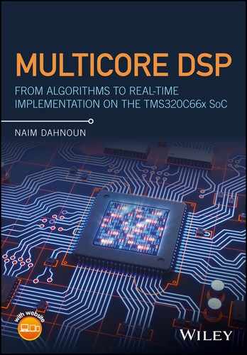
Building on a previous success with the first digital signal processor (DSP) generation based on the Texas Instruments (TI) VelociTITM architecture TMS320C6000, which used an enhancement of the VLIW (very long instruction word) architecture, TI has now pushed the frontiers a bit further by embracing the multicore system‐on‐chip (SoC) technology and adding many features, such as: enhanced architecture, more configurable coprocessors, tiered memory architecture, high speed, a low‐latency point‐to‐point communication interface known as the HyperLink, a TeraNet switch fabric which provides fast interconnection between the DSP CorePacs, the ARM CorePacs when available, memory, peripherals and a Multicore Navigator that can provide high‐speed packed data movement without CPU loading, to create the new generation known as the TMS320C66x. See the TI DSP roadmap in Figure 2.1.
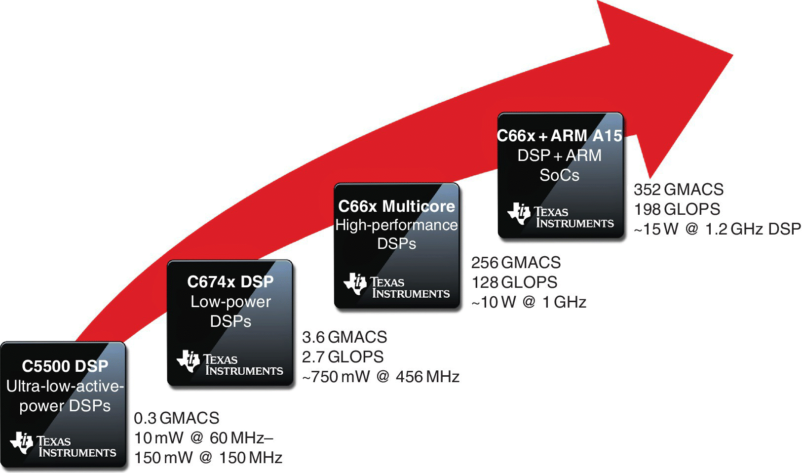
Figure 2.1 Texas Instruments (TI) digital signal processor (DSP) roadmap.
The TMS320C66x devices support both fixed‐ and floating‐point arithmetic that can be mixed in order to combine low power and large dynamic range. The TMS320C66x is composed of four main parts: the CPUs, memories, peripherals and coprocessors, all connected by various buses as shown in Figure 2.2 and Figure 2.3.
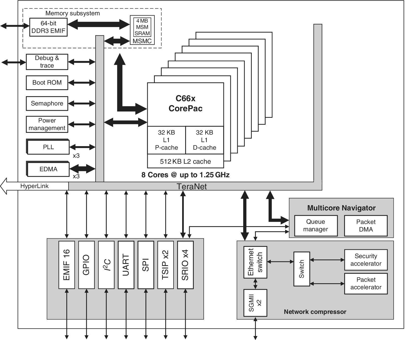
Figure 2.2 KeyStone I architecture [3].
Figure 2.3 KeyStone II architecture [4].
At the time of writing this chapter, the TMS320C66x processors were divided into two families: the KeyStone I (see Table 2.1) and the KeyStone II (see Table 2.2). The KeyStone II family incorporates ARM cores in addition to DSP cores (known as CorePacs). A document on migration from KeyStone I to KeyStone II can be found in Ref. [1].
Table 2.1 KeyStone I family
| C6678 | C6674 | C6657 | C6655 | C6654 | C6652 | |
| MHz per core | 1–1.25 GHz | 1–1.25 GHz | 1–1.25 GHz | 1–1.25 GHz | 750–850 MHz | 600 MHz |
| Number of cores | 8 | 4 | 2 | 1 | 1 | 1 |
| Max GMACs | 320 (@1.25 GHz) | 160 (@1.25 GHz) | 80 (@1.25 GHz) | 40 (@1.25 GHz) | 27.2 (@850 MHz) | 19.2 (@600 MHz) |
| Max GFLOPs | 160 @ 1.25 GHz | 80 @ 1.25 GHz | 40 @ 1.25 GHz | 20 @ 1.25 GHz |
13.6 @ 850 MHz | 9.6@ 600 MHz |
Table 2.2 KeyStone II family
| 66AK2G02 | 66AK2 E02 |
66AK2 E05 |
66AK2 L06 |
66AK2 H06 |
66AK2 H12 |
66AK2 H14 |
||
| Number of cores (maximum frequency) |
ARM Cortex‐A15 | 1 (600 MHz) |
1 (1.4 GHz) |
4 (1.4 GHz) |
2 (1.2 GHz) |
2 (1.4 GHz) |
4 (1.4 GHz) |
4 (1.4 GHz) |
| C66x DSP | 1 (600 MHz) |
1 (1.4 GHz) |
1 (1.2 GHz) |
4 (1.2 GHz) |
4 (1.2 GHz) |
8 (1.2 GHz) |
8 (1.2 GHz) |
|
| Performance | GFLOPs | 28.8 | 33.6 | 67.2 | 69.0 | 99.2 | 198.4 | 198.4 |
| GMACs | 19.2 | 44.8 | 44.8 | 153.6 | 153.6 | 307.2 | 307.2 | |
The KeyStone I (Figure 2.2) can be clocked from 600 MHz to 1.25 GHz depending on the device used; see Table 2.1. For the KeyStone II (Figure 2.3), both DSP and ARM cores can be clocked from 600 MHz to 1.4 GHz; see Table 2.2. The TMS320C66x CorePacs are an improved version of the C6000 CPUs covered in detail in Ref. [2].
2.2 The CPU
The TM320C66x CPUs are composed of two blocks known as data path 1 and data path 2, as shown in Figure 2.4. Each block has four execution units known as .L (logical unit), .M (multiplier unit), .S (shift unit) and .D (data unit) that can run in parallel; a register file containing 32 32‐bit general‐purpose registers; and multiple paths for (1) data communications between each block and memory, (2) data communications within each block or (3) data communications between blocks.
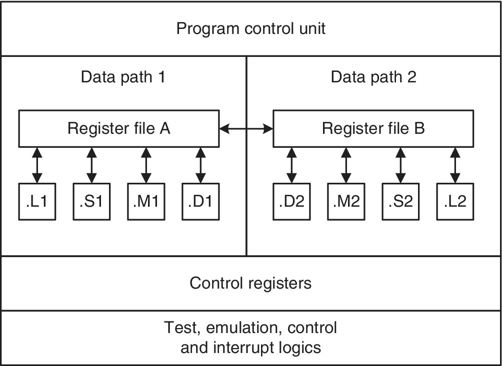
Figure 2.4 TMS320C66x CPU block diagram.
From Figure 2.5, it can be seen that register file A can be written to or read from functional units .L1, .S1, .M1 and .D1 via the paths indicated by arrows. The same can be applied to register file B where all registers can be accessed by functional units .L2, .S2, .M2 and .D2. The CPU paths can be divided into two types: one is the data path, and the other is the address path. The data paths are used for data transfer between the register files and the units, or data transfer between the memory and the register files. However, the address path is used for sending the address from the data unit .D to the memory.
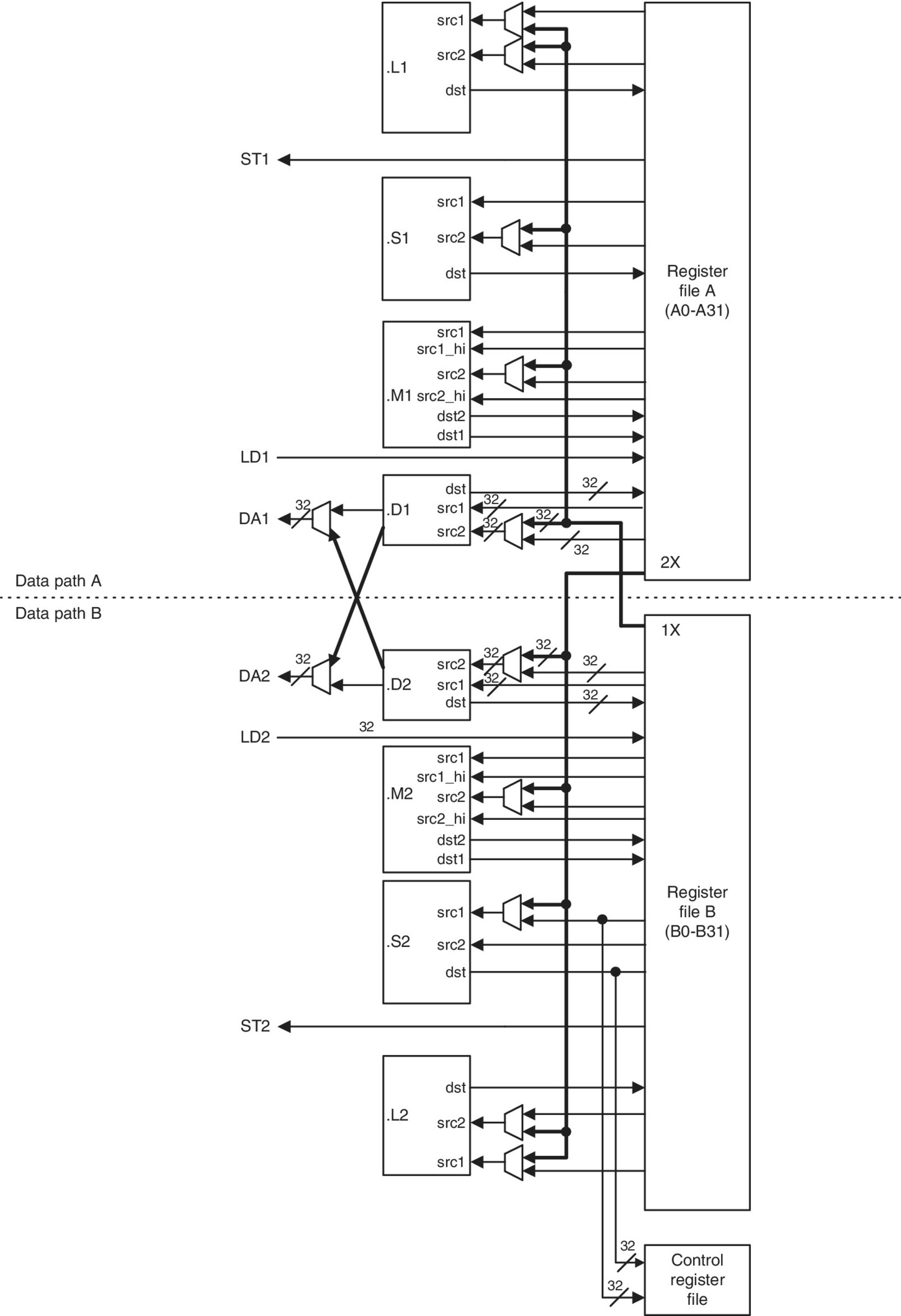
Figure 2.5 TMS320C66x CPU data path and control.
The challenge for optimising code on this processor is to make use of all units for every cycle. This is discussed in Chapter 5.
2.2.1 Cross paths
Cross paths enable linking of one side of the CPU (e.g. data path A) to the other (e.g. data path B). These are shown in bold arrows in Figure 2.5. Although the cross paths are useful in terms of the flexibility in using units with two or multiple operands from both sides of the CPU, there are restrictions which are discussed in this section.
2.2.1.1 Data cross paths
The data cross paths are also referred to as the register file cross paths. These cross paths allow up to 64‐bit operands from one side to cross to the other side. There are only two cross paths: one from side B to side A (1X), and one from side A to side B (2X). These limit the number of cross paths to two for each execute packet (instructions in parallel form an execute packet). The following points must be observed:
- Only one cross path per direction per execute packet is permitted.
- The destination register is always on the same side of the unit used.
2.2.1.2 Address cross paths
The addresses generated by the data unit .D1 and .D2 can be sent to either the data address path DA1 or the data address path DA2, as shown in bold arrows in Figure 2.5. The advantages of using an address cross path are to be able to generate the address using one register file, and to access the data from the other register file as illustrated in Figure 2.6. Here again, there are only two cross paths for each execute packet and the following points should be observed:
- Only one address cross path per direction per execute packet is allowed.
- When an address cross path is used, the destination register for the load (LD) instructions and the source register for the store (ST) instructions should come from the opposite side of the unit (see Figure 2.6), or simply the register pointers must come from the same side of the .D unit used.
- If both .D units are to be used, then either none or both of the address cross paths should be used.

Figure 2.6 Address cross paths.
2.2.2 Register file A and file B
This processor is a reduced instruction set computer (RISC)‐like processor, and all operands are specified in registers except for the n‐bit constants. There are two register files each containing 32 32‐bit registers.
2.2.2.1 Operands
An operand can be an n‐bit constant or a 32‐bit register, two 32‐bit registers or four 32‐bit registers, depending on the instruction:
- Constant
- 32‐bit registers
- 64‐bit registers
- 128‐bit registers.
To create 40‐ or 64‐bit operands, two registers have to be concatenated; see Table 2.3. To create a 128‐bit operand, four registers have to be concatenated; see Table 2.4. The registers must be:
- From the same side
- Consecutively ordered
- Ordered as even‐odd from right to left for the 64‐bit, as shown in Table 2.3, and ordered even‐odd‐even‐odd from right to left for the 128‐bit, as shown in Table 2.4.
Table 2.3 Possible 40‐/64‐bit register pair combinations
| Register file A | Register file B |
| A1:A0 | B1:B0 |
| A3:A2 | B3:B2 |
| A5:A4 | B5:B4 |
| A7:A6 | B7:B6 |
| A9:A8 | B9:B8 |
| A11:A10 | B11:B10 |
| A13:A12 | B13:B12 |
| A15:A14 | B15:B14 |
Table 2.4 Possible 128‐bit register pair combinations
| Register file A | Register file B |
| A3:A2:A1:A0 | B3:B2:B1:B0 |
| A7:A6:A5:A4 | B7:B6:B5:B4 |
| A11:A10:A9:A8 | B11:B10:B9:B8 |
| A15:A14:A13:A12 | B15:B14:B13:B12 |
| A19:A18:A17:A16 | B19:B18:B17:B16 |
| A23:A22:A21:A20 | B23:B22:B21:B20 |
| A27:A26:A25:A24 | B27:B26:B25:B24 |
| A31:A30:A29:A28 | B31:B30:B29:B28 |
2.2.3 Functional units
The four types of units (.M, .L, .S and .D) are designed to perform different operations. However, some operations can be performed with different units; for instance, the ADD instruction can be performed by the .L units, the .S units or the .D units. The TMS320C66x DSP CPU and Instruction Set Reference Guide [5] should be consulted before using an instruction.
The assembly syntax for this DSP core is as follows:
| |condition| | instruction | .unit | operand 1, | operand 2, | destination | ; comments |
Example:
|B0| ADD.S1 A0,A1,A2 ; commentswhere:
- |B0|: If B0 is not equal to zero, then execute the instruction ‘ADD .S1 A0,A1,A2’.
- ADD .S1 A0,A1,A2: Add A0 and A1, and store the result to register A2.
- ; comments: Used for comments and therefore not assembled.
2.2.3.1 Condition registers
- The condition can be one of the following registers: A0, A1, A2, B0, B1 or B2.
- Most instructions can be conditional.
- The specified condition register is tested at the beginning of the E1 pipeline stage for all instructions. Refer to the user guide [5] for the pipeline operations.
- Compact (16‐bit) instructions on the DSP always execute unconditionally. See ‘Compact instructions on the CPU’ in Ref. [5].
The condition can be inverted by adding the exclamation symbol ‘!’ as follows:
|!B0| ADD.S1 A0,A1,A2where:
- |!B0|: If B0 is equal to zero, then execute the instruction ‘ADD .S1 A0,A1,A2’.
2.2.3.2 .L units
The .L units support up to 64‐bit operands. All instructions using these units complete in one cycle.
The .L unit can perform:
- Arithmetic operations (floating or fixed point)
- Logical operations
- Branch functions
- Data‐packing operations
- Conversion to/from integer and single‐precision values.
The .L unit has additional instructions for logical AND and OR instructions, as well as 90 degree or 270 degree rotation of complex numbers (up to two per cycle) [5].
Examples using the .L1 unit:
| Example 1 | AND | .L1 | A1:A0,A3:A2,A9:A8 | ; AND 64‐bit and 64‐bit |
| Example 2 | AND | .L1 | A0,A1,A2 | ; AND 32‐bit and 32‐bit |
| Example 3 | AND | .L1 | 0x9,A0,A2 | ; AND 5‐bit constant (scst5) and 32‐bit |
2.2.3.3 .M units
There are two hardware multiplier units, .M1 (for data path 1) and .M2 (for data path 2), that can perform fixed‐point or floating‐point multiplications as shown in Table 2.5 and Table 2.6. The .M units support 128‐bit.
Table 2.5 Fixed‐point multiplications per unit
|
Table 2.6 Floating‐point multiplications per unit
|
As stated earlier, the instructions load, store, multiply and branch have different latencies and therefore complicate programming. All TMS320C66x instructions require only one cycle to execute (unit latency is one). However, some results are delayed (delay slots). When instructions are pipelined, the multiplier can issue one instruction per cycle.
Care should be taken when using the .M units to perform operations other than multiplications. Each .M unit has two 64‐bit write ports to the register file, and therefore the results of a 4‐cycle instruction and a 2‐cycle instruction operating on the same .M unit can write their results on the same instruction cycle. This is not an issue as long as the programmer is aware of this; see the example in Figure 2.7.
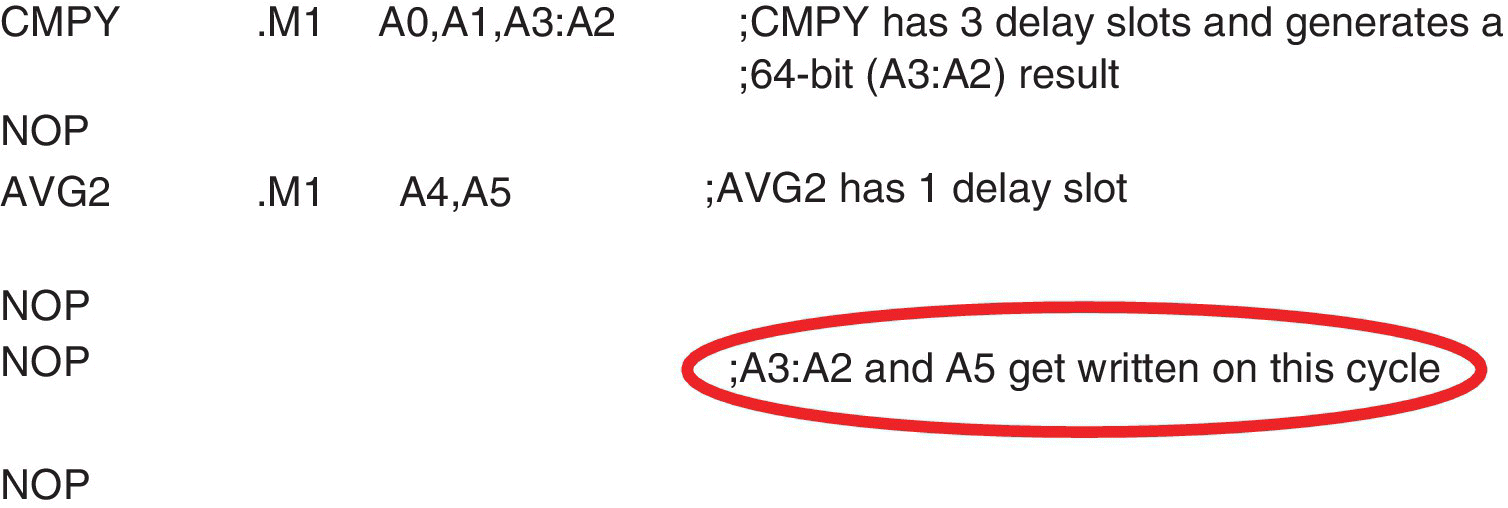
Figure 2.7 Instructions completing in the same cycle.
2.2.3.4 .S units
These units (.S1 and .S2) contain 32‐bit integer ALUs (arithmetic and logic units) and 40‐bit shifters. They can be used for:
- 32‐bit arithmetic, logic and bit field operations
- 32/40‐bit shifts
- Branches
- Transfer to and from control registers (.S2 only)
- Constant generation.
Note: All instructions executing in the .L or .S are single‐cycle instructions, except for the branch instructions.
2.2.3.5 .D units
The data units (.D1 and .D2) are the only units that can be used for accessing memory. They can be used for the following operations:
- Load and store with 5‐bit constant offset
- Load and store with 15‐bit constant offset (.D2 only)
- 32‐bit additions and subtractions
- Linear and circular address calculations
- Logical operations
- Moving a constant or data from a register to another register.
2.3 Single instruction, multiple data (SIMD) instructions
To make maximum use of the units and therefore increase the performance, one should exploit the SIMD operations available with the TMS320C66x. Figure 2.8 shows an example of a 4‐way SIMD with an instruction α operating on multiple data from Src1 and Src2 to produce multiple data on the Dst.
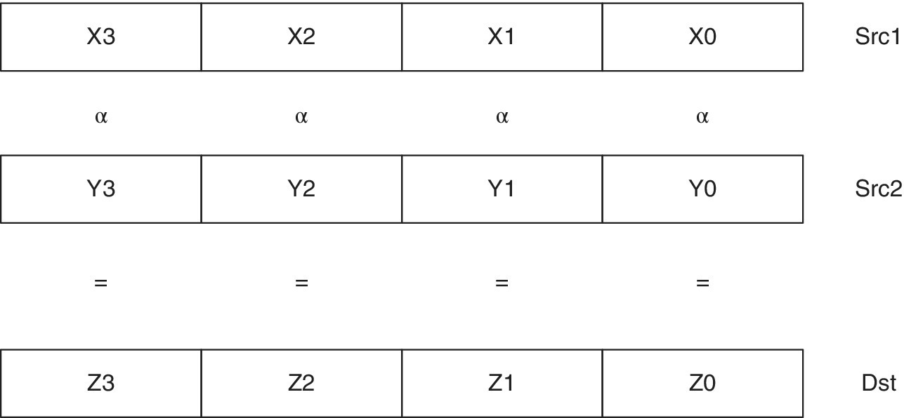
Figure 2.8 Four‐way SIMD operation.
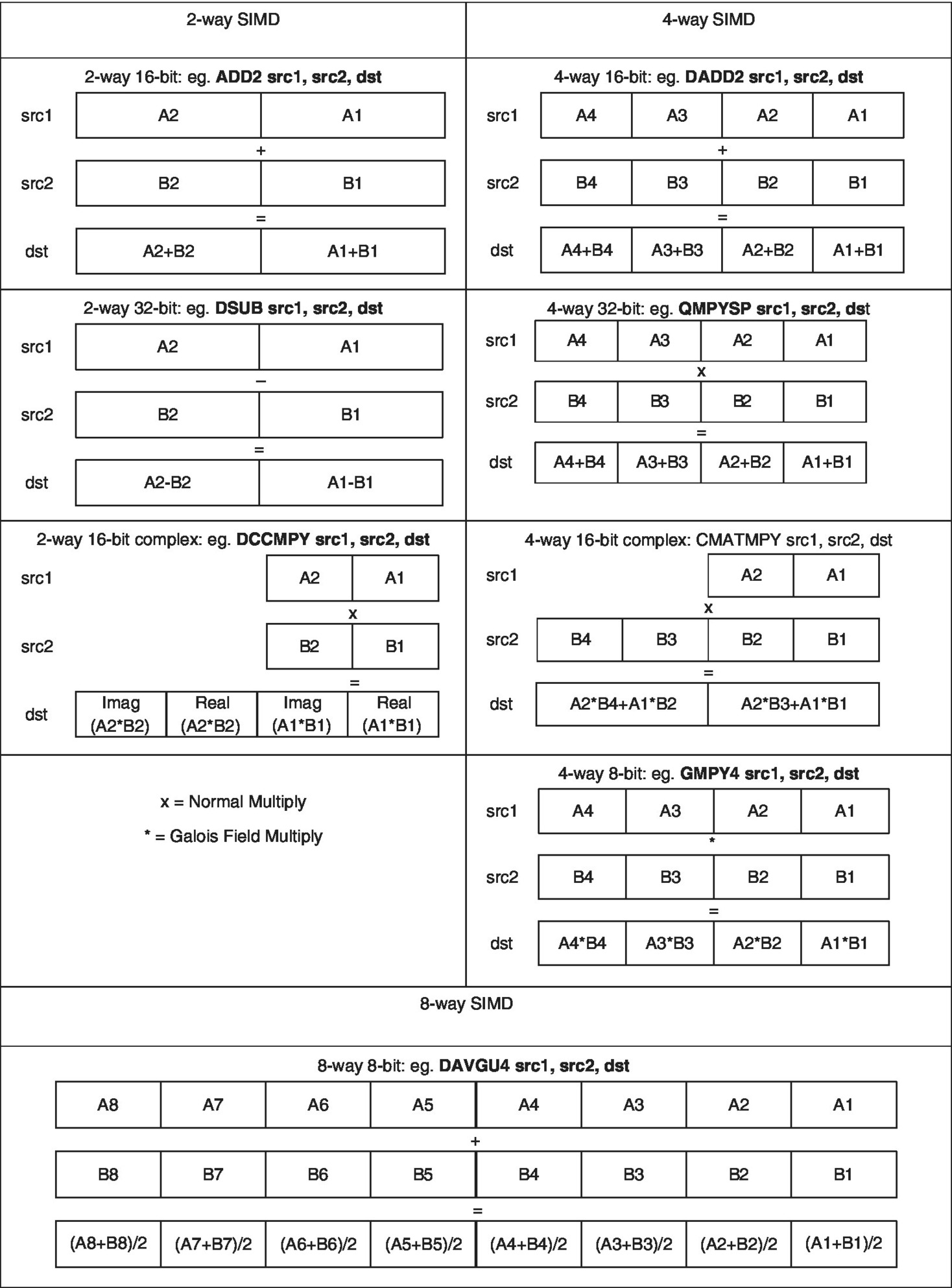
TMS320C66x supports 2‐way, 4‐way and 8‐way SIMD operating on 8‐bit, 16‐bit, 32‐bit, 64‐bit or 128‐bit, depending on the instruction used. Examples with different ways are shown in Table 2.7.
Table 2.7 SIMD examples
2.3.1 Control registers
The TMS320C66x devices have a number of registers for control purposes; see Table 2.8. Reading and writing to the control registers can be performed only via the .S2 unit. All control registers can be accessed by only the MVC (move constant) instruction.
Note: Only the .S2 unit and the MVC instruction can be used to access the control registers. However, some bit fields in some control registers can be modified by some instructions or events. For instance, when an interrupt occurs, a bit field in the Interrupt Flag Register (IFR) register will be modified.
Table 2.8 TMS320C66x control registers [5]
| Acronym | Register |
| AMR | Addressing mode register |
| CSR | Control status register |
| GFPGFR | Galois field multiply control register |
| ICR | Interrupt clear register |
| IER | Interrupt enable register |
| IFR | Interrupt flag register |
| IRP | Interrupt return pointer register |
| ISR | Interrupt set register |
| ISTP | Interrupt service table pointer register |
| NRP | Non‐maskable interrupt (NMI) return pointer register |
| PCE1 | Program counter, E1 phase |
| Control register file extensions | |
| DNUM | DSP core number register |
| ECR | Exception clear register |
| FR | Exception flag register |
| GPLYA | GMPY A‐side polynomial register |
| GPLYB | GMPY B‐side polynomial register |
| IERR | Internal exception report register |
| ILC | Inner loop count register |
| ITSR | Interrupt task state register |
| NTSR | NMI/exception task state register |
| REP | Restricted entry point address register |
| RILC | Reload inner loop count register |
| SSR | Saturation status register |
| TSCH | Time‐stamp counter (high 32) register |
| TSCL | Time‐stamp counter (low 32) register |
| TSR | Task state register |
| Control register file extensions for floating‐point operations | |
| FADCR | Floating‐point adder configuration register |
| FAUCR | Floating‐point auxiliary configuration register |
| FMCR | Floating‐point multiplier configuration register |
2.4 The KeyStone memory
Memory is one of the predominant factors that establishes the final performance of any processor. In fact, the embedded memory system is one of the items that determines the system performance, efficiency, size and cost. The design of the memory (internal or external), the memory controller that manages the data flow and the buses that transport these data are very important for an efficient delivery of data at the bandwidth, latency and power required. In fact, the memory die takes more than 50% of the total area of a typical SoC. The TMS320C66x memory architecture is organised as shown in Figure 2.9. Each core has its own local level 1 memory (L1 Data Cache and L1 Program Cache) and its own local level 2 memory. Both local levels can be configured as memory‐mapped SRAM, cache or a combination of SRAM and cache. Coherency is maintained between L1 and L2 for each core, as highlighted in Figure 2.9.
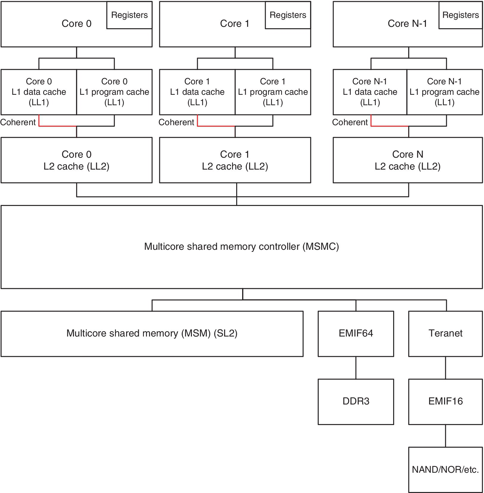
Figure 2.9 Simplified memory structure for KeyStone.
The Multicore Shared Memory Controller (MSMC) allows all cores access to the shared memory (SL2) and the external memory. Note that the external memory is accessed via the external memory interface (EMIF) or the TeraNet. Multiple EMIFs may be available, depending on the device used.
The shared memory referred to in Figure 2.2 and Figure 2.3 as the SRAM is the MSMC that can be configured as shared memory SL2 or a shared memory level 3 (SL3), as shown in Figure 2.9.
When the SRAM is configured as SL2, this memory will be cacheable with L1D and L1P memories.
When the SRAM is configured as SL3, this memory will be cacheable with both L1 and L2 memories.
Although the SL2 memory appears in Figure 2.9 as level 3, its performance is the same as that of the LL2 due to the optimal prefetching capability of the extended memory controllers (XMCs) that are placed within the cores (see Figure 2.10); hence it is called level 2.
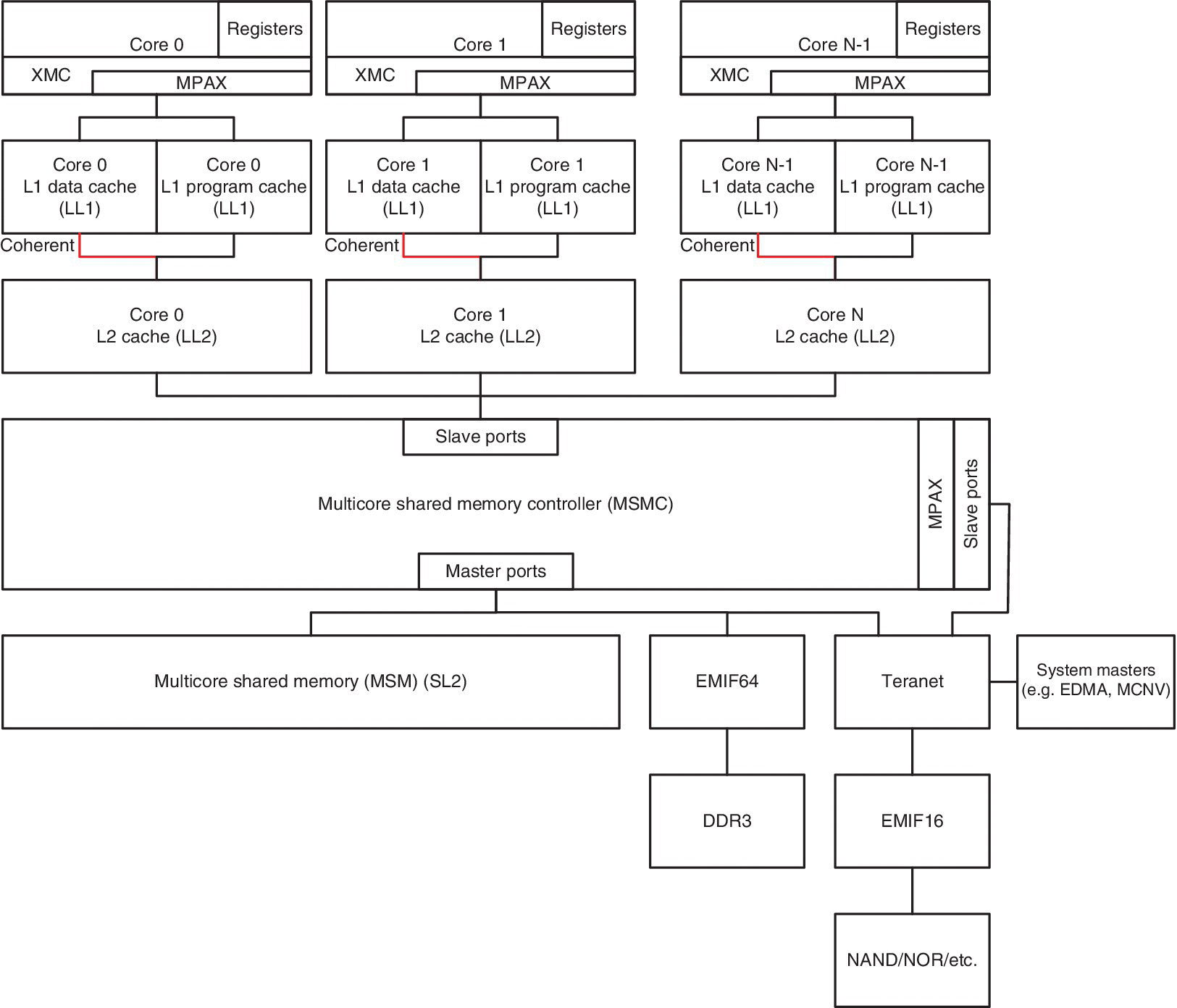
Figure 2.10 Memory structure, including the MPAX for KeyStone.
2.4.1 Using the internal memory
When writing an application for a multicore processor, one tends to write code for one core and then run it in all cores. This simple task can be complicated to write as the local memories will have to have different addresses. For instance, the L2 SRAMs for the TMS320C6678 shown in Table 2.9 have different addresses. However, in a practical situation, each core sees its addresses differently. In the example shown in Figure 2.11, all cores use the same starting address 0 × 0080 0000 to access their local memories. For example, Core 0 can access the local memory of Core 1 by using the address 0 × 1180 0000, and Core 7 accessing the local memory L2 of Core 5 by using the address 0 × 1580 0000 and so on. In this way, a single code can be used by all cores without modifications.
Table 2.9 Local L2 memory for all TMS320C6678 cores
| Core 0: 0 × 1080 0000 to 0 × 0087 FFFF Core 1: 0 × 1180 0000 to 0 × 1187 FFFF Core 2: 0 × 1280 0000 to 0 × 1287 FFFF Core 3: 0 × 1380 0000 to 0 × 1387 FFFF Core 4: 0 × 1480 0000 to 0 × 1487 FFFF Core 5: 0 × 1580 0000 to 0 × 1587 FFFF Core 6: 0 × 1680 0000 to 0 × 1687 FFFF Core 7: 0 × 1780 0000 to 0 × 1787 FFFF |

Figure 2.11 Example of cores accessing their local or other local memories.
2.4.2 Memory protection and extension
It has been shown that each core can use its own local memory (LL1, LL2, LS2 or LS3), and it has also been shown that cores can use the same code and the same addresses for accessing local variables. However, when data and/or code cannot fit in the internal memory, code and/or data will have to be located in the DDR memory. In this case, data and/or code located in the DDR will need to be accessed with different addresses unless they are shared. The Memory Protection and Address Extension (MPAX) unit can be used to make portions of the DDR look like local memories. For instance, if we consider the situation where Core 1 and Core 2 have the same code but different data (data 1 for Core 1 and data 2 for Core 2) and both code and data do not fit in the internal memory, one can use the MPAX registers to configure part of the DDR as a private memory to each core and part as shared memory, as shown in Figure 2.12. This has the advantage of increasing the performance, as no software is required to do the address translation and the same code is used by all cores. However, by doing so, the cache coherency must be maintained ‘manually’ by using the cache invalidate, cache writeback and cache writeback‐invalidate, since there is no coherency between the external memory and the internal memory. In addition to address extension, the MPAX can also be used for internal and external memory protection. More details covering the MPAX can be found in Refs. [6] and [7].
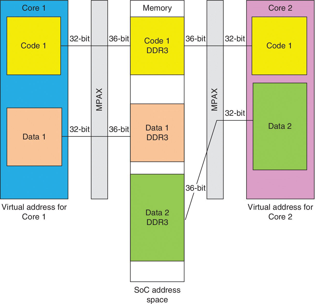
Figure 2.12 Example showing the use of MPAX.
2.4.3 Memory throughput
Knowing where to locate the program and data is very critical for performance. In this section, the maximum data throughput is highlighted.
Consider Figure 2.13, and be aware that the DSP cores for the TMS320C6678 can be clocked at 1.0 GHz, 1.25 GHz or 1.4 GHz. Let’s assume that a core is clocked at 1.0 GHz and calculate the memory throughput.
- L1D SRAM. This operates at the same frequency as the DSP core and can access a maximum of 128‐bit data. Therefore, the throughput is 16 GB/s [(128) * (1.0)/8].
- L1P SRAM. This operates at the DSP clock frequency, and the CPU can fetch up to 256‐bit instructions. Therefore, the throughput is 32 GB/s [(256 * (1.0)/8)].
- L2 SRAM. This operates at half the frequency of the DSP core and can access a maximum of 256‐bit data. Therefore, the throughput will be half of the L1D SRAM, that is, 16 GB/s [(256 * (0.5)/8].
- MSMC SRAM. Operates at half the frequency of the DSP core but has four banks that can be accessed simultaneously. Therefore, the aggregate throughput will be four times that of the L2 SDRAM, which is 64 GB/s. Each KeyStone DSP core has a 256‐bit path at half the DSP clock frequency for a throughput of 16 GB/s. The KeyStone II doubles the clock speed and throughput.
- DDR3. The DDR3 has a 64‐bit interface to the MSMC and can be clocked at a maximum frequency of 1.333 GHz; therefore, the throughput is 10.666 GB/s (64 * 1.333)/8).
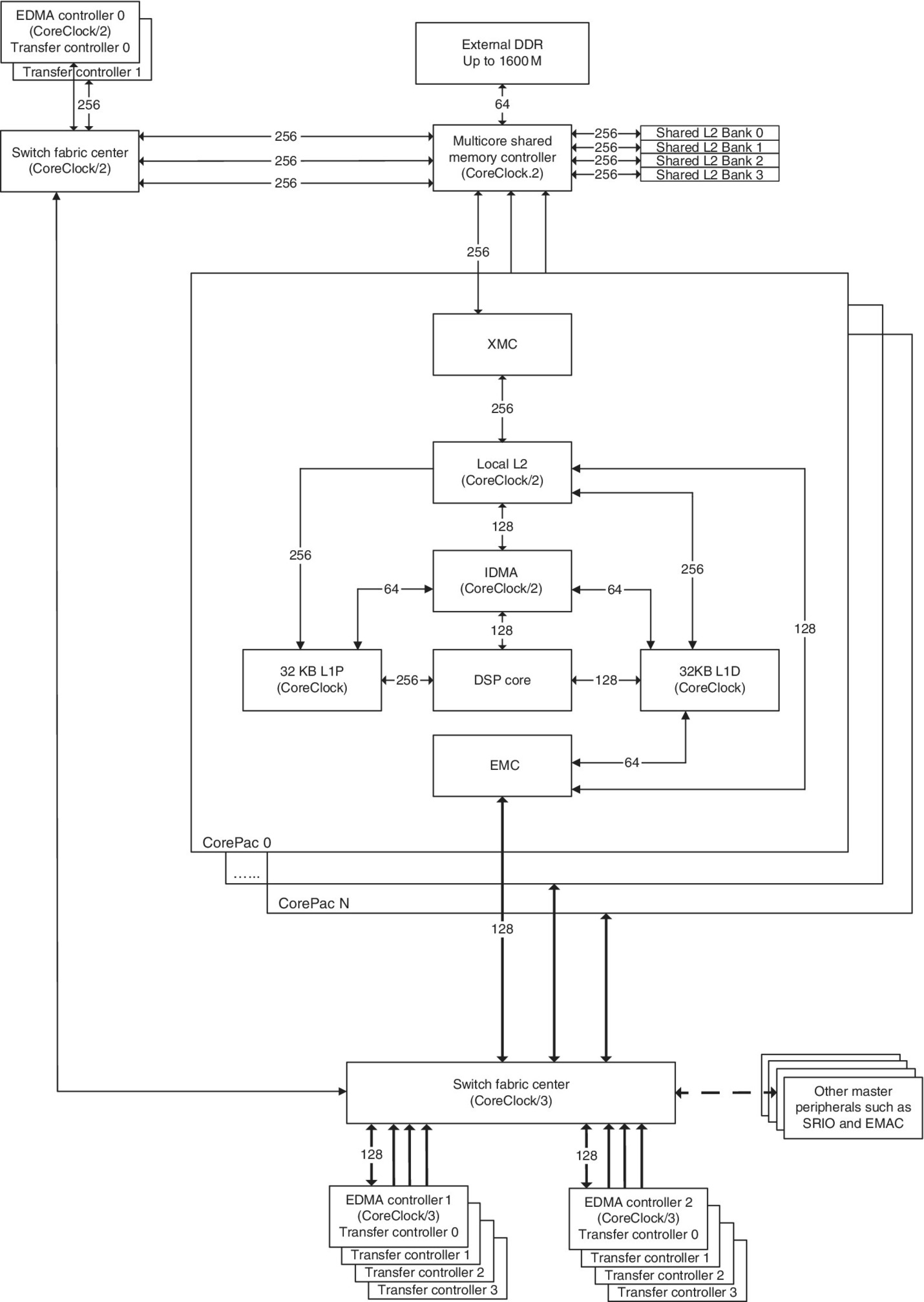
Figure 2.13 Memory topology for the TMS320C6678.
It is also important to explore and contrast the data throughput using the CPU (as shown here) and the EDMA; see Ref. [8].
For the KeyStone II device throughput, refer to Ref. [9].
2.5 Peripherals
The KeyStone I and II have a rich set of peripherals that are shown in Figure 2.2 and Figure 2.3, respectively. Each peripheral is described in a user guide. The peripherals used in this book are summarised in this section.
2.5.1 Navigator
The Multicore Navigator, also referred to as the Navigator, provides a high‐speed packed data transfer to enhance CorePac to accelerator/peripheral data movements, core‐to‐core data movements, inter‐core communication and synchronisation without loading the CorePacs. The Navigator is covered in Chapter 14.
2.5.2 Enhanced Direct Memory Access (EDMA) Controller
The TMS320C66x on‐chip EDMA Controller allows data transfers between the internal memory and (1) external memory, (2) host port and (3) external peripherals. The EDMA data transfer is performed with zero overhead and is transparent to the CPU, which means that the EDMA and the CPU operations can be independent. Of course, if both the DMA and the CPU try to access the same memory location, arbitration will be performed by the program memory controller. The EDMA is covered in Chapter 8 and in the EDMA user guide [10].
2.5.3 Universal Asynchronous Receiver/Transmitter (UART)
The UART on the KeyStone I and II is full duplex. The UART has a programmable baud rate, and both transmit and receive sides have FIFOs (first in, first out) that can store 16 bytes to ease the pressure on the CPU. These FIFOs can be bypassed. The TMS320C6678 has one UART, and the TMS32066AK2H14/12/06 has two UARTs. An example showing how to use and program these UARTs can be found in Chapter 15. More information can be found in the UART user guide [11].
2.5.4 General purpose input–output (GPIO)
The KeyStone I and II both have several GPIO pins (the TMS320C6678 has 16 GPIO pins, and the TMS320C66AK2H14/12/06 has 32 pins) that can be configured to be inputs or outputs. To provide flexibility, each GPIO pin can be controlled independently. These pins can be programmed to generate interrupts to the CPU or the EDMAs on the rising or falling edge. Chapter 6 provides examples with GPIOs for generating interrupts. More information can be found in the ‘KeyStone Architecture General Purpose Input/Output (GPIO) User Guide’ [12].
2.5.5 Internal timers
The TMS320C6678 has 16 32‐bit timers, and the 66AK2H14/12 has 20 32‐bit programmable internal timers. Each core (DSP or ARM) has its own timer that can be configured as a general‐purpose timer or a watchdog timer, and the rest of the timers can only be configured as general‐purpose timers.
A timer is composed of one 64‐bit timer period register to host the count value specified by the user and one count‐up (timer counter) register that is incremented in every input clock. When the timer counter reaches the timer period register value, it either will trigger a timer interrupt to the CPU, trigger a timer event to the EDMA controller, set a bit in the TCR register or generate an output signal on the timer output pin.
The timers can be configured as single 64‐bit timers or dual 32‐bit timers that can operate as chained (chained mode), where one timer triggers the other which then generates the interrupt signals, or operate as unchained (unchained mode), where both timers can generate interrupts. The timers can also be configured to be used as 64‐bit watchdog timers in order to provide a control exit; see Table 2.10. More details can be found in Ref. [13]. See Chapter 7 for examples using the timers.
Table 2.10 Timer modes
| 64‐bit general‐purpose timer (default) |
| Dual 32‐bit timers (unchained) |
| Dual 32‐bit timers (chained) |
| 64‐bit watchdog timer |
2.6 Conclusion
To get maximum performance from each DSP core, one should understand the architecture very well. It has been shown that each core has eight units, and the algorithm must make use of all these units as much as possible to extract maximum performance. To further exploit these units, SIMD operations should be used when feasible.
Understanding the operations of peripherals to use and the memory layout is important for developing applications with the required functionalities and performance.
References
- 1 Texas Instruments, KeyStone I‐to‐KeyStone II migration guide: SPRABW9A, July 2015. [Online]. Available: http://www.ti.com/lit/an/sprabw9a/sprabw9a.pdf. [Accessed 2 December 2016].
- 2 N. Dahnoun, Digital Signal Processing Implementation Using the TMS320C6000 DSP Platform, Reading, MA: Addison‐Wesley Longman, 2000.
- 3 Texas Instruments, Multicore fixed and floating‐point digital signal processor, March 2014. [Online]. Available: http://www.ti.com/lit/ds/symlink/tms320c6678.pdf. [Accessed 2 December 2016].
- 4 Texas Instruments, Multicore DSP + ARM KeyStone II System‐on‐Chip (SoC), November 2013. [Online]. Available: http://www.ti.com/lit/ds/symlink/66ak2h12.pdf. [Accessed 2 December 2016].
- 5 Texas Instruments, TMS320C66x DSP CPU and instruction set reference guide, November 2010. [Online]. Available: http://www.ti.com/lit/ug/sprugh7/sprugh7.pdf. [Accessed 2 December 2016].
- 6 Texas Instruments, TMS320C66x DSP CorePac user guide, July 2013. [Online]. Available: http://www.ti.com/lit/ug/sprugw0c/sprugw0c.pdf. [Accessed 2 December 2016].
- 7 Texas Instruments, KeyStone memory architecture, 2010. [Online]. Available: http://www.ti.com/lit/wp/spry150a/spry150a.pdf. [Accessed 2 December 2016].
- 8 Texas Instruments, TMS320C6678 memory access performance, April 2011. [Online]. Available: http://www.deyisupport.com/cfs‐file.ashx/__key/telligent‐evolution‐components‐attachments/00‐53‐00‐00‐00‐02‐19‐24/TMS320C6678_5F00_Memory_5F00_Access_5F00_Performance.pdf. [Accessed 2 December 2016].
- 9 Throughput performance guide for KeyStone II devices, Texas Instruments, December 2015. [Online]. Available: http://www.ti.com/lit/an/sprabk5b/sprabk5b.pdf. [Accessed January 2017].
- 10 Texas Instruments, KeyStone Architecture Enhanced Direct Memory Access (EDMA3) Controller user's guide, May 2015. [Online]. Available: http://www.ti.com/lit/ug/sprugs5b/sprugs5b.pdf. [Accessed 2 December 2016].
- 11 Texas Instruments, KeyStone architecture Universal Asynchronous Receiver/Transmitter (UART) user guide, November 2010. [Online]. Available: http://www.ti.com/lit/ug/sprugp1/sprugp1.pdf. [Accessed 2 December 2016].
- 12 Texas Instruments, KeyStone architecture general purpose input/output (GPIO) user guide, November 2010. [Online]. Available: http://www.ti.com/lit/ug/sprugv1/sprugv1.pdf. [Accessed 2 December 2016].
- 13 Texas Instruments, KeyStone Architecture TIMER64P user guide, March 2012. [Online]. Available: http://www.ti.com/lit/ug/sprugv5a/sprugv5a.pdf. [Accessed 2 December 2016].