
6
The TMS320C66x interrupts
6.1 Introduction
As with most microprocessors, the TMS320C66x allows normal program flow to be interrupted. In response to the interruption, the CPU finishes executing the current instruction(s) and branches to a procedure which services the interrupt. To service an interrupt, the user or the system must save the contents of the registers and the context of the current process, then service the interrupt task, restore the registers and the context of the process, and finally resume the original process (see Figure 6.1). The interrupt can come from an external device, an internal peripheral or simply a special instruction in the program.

Figure 6.1 Interrupt response procedure.
There are four types of interrupts on the TMS320CC66x CPUs. These are the two non‐maskable interrupts (Reset and NMI) and maskable interrupts (EXCEP and INT4–INT15) (see Figure 6.2 and Table 6.1). The interrupt controllers described in this chapter allow events to be mapped to any of the input interrupts from INT4 to INT15.

Figure 6.2 Various interrupts available.
Table 6.1 Interrupt sources and priority
| Type | Interrupt name | Priority |
| Non‐maskable | Highest | |
| NMI | ||
| Maskable | EXCEP | |
| INT4 | ||
| INT5 | ||
| INT6 | ||
| INT7 | ||
| INT8 | ||
| INT9 | ||
| INT10 | ||
| INT11 | ||
| INT12 | ||
| INT13 | ||
| INT14 | ||
| INT15 | Lowest |
Due to the sheer number of events available (hundreds) and the low number of interrupts that the CPU, Enhanced Direct Memory Access (EDMA) or hyperlink can handle, some events are aggregated first by the chip‐level interrupt controllers (CICs or CpIntcs) to generate the secondary events. The other events are unchanged and are called primary events. Secondary events are infrequent events and are routed to the CIC first to offload the interrupt controller (INTC) as shown in Figure 6.3.
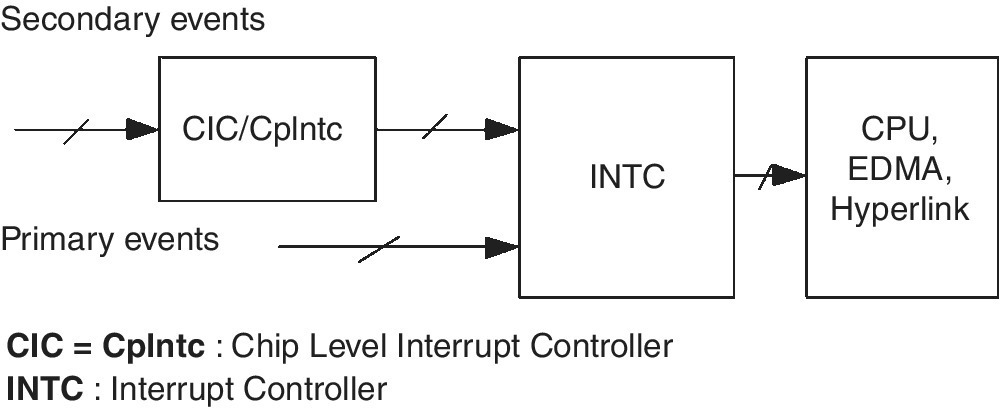
Figure 6.3 Interrupts: the big picture.
Each processor has a fixed number of CICs. For instance, the TMS320C6678 has four CICs and the 66AK2H14/12 has only three CICs; see Figure 6.4 or 6.5. As can be seen from these figures, each event (primary or secondary) is mapped to a specific core or peripheral. However, some events are broadcast to many cores.

Figure 6.4 CIC controllers for the TMS32C6678 [1].

Figure 6.5 CIC controller for the 66AK2H14/12 [2].
The primary task of the user is to identify which event or events are to be programmed to generate an interrupt. Each event is identified by a number and described in the user guide. A sample of events available is shown in Table 6.2. Let’s now examine the CIC.
Table 6.2 CIC0 event inputs (secondary interrupts for TMS320C66x CorePacs) [1]
| Input event no. on CIC | System interrupt | Description |
| 0 | EDMA3CC1 CC_ERRINT | EDMA3CC1 error interrupt |
| 1 | EDMA3CC1 CC_MPINT | EDMA3CC1 memory protection interrupt |
| 2 | EDMA3CC1 TC_ERRINT0 | EDMA3CC1 TC0 error interrupt |
| – – |
– – |
– – |
| 38 | EDMA3CC0 CCINT0 | EDMA3CC0 individual completion interrupt |
| 39 | EDMA3CC0 CCINT1 | EDMA3CC0 individual completion interrupt |
| 40 | EDMA3CC0 CCINT2 | EDMA3CC0 individual completion interrupt |
| – – |
– – |
– – |
| 157 | QM_INT_PASS_TXQ_PEND_23 | Queue manager pending event |
| 158 | QM_INT_PASS_TXQ_PEND_24 | Queue manager pending event |
| 159 | QM_INT_PASS_TXQ_PEND_25 | Queue manager pending event |
6.1.1 Chip‐level interrupt controller
A CIC (see Figures 6.3, 6.4 and 6.5) accepts system‐level events (see datasheet for a particular device) and combines them to generate secondary events to the interrupt controller, as shown in Figure 6.3. Figure 6.4 shows that the TMS320C6678 has four CICs (CIC0, CIC1, CIC2 and CIC3) responding to various events (some events can be found in different CICs).
The CICs are composed of:
- An enabler. The enabler is used to enable or disable an event. This event will be logged in the interrupt status register. If the event was enabled and the event happened, the Enabled Status will be set. If the event happens and the event was disabled, the event will be logged in the Raw Status and not in the Enable Status; see Figure 6.6. The Enabled Status can also be set by software, which is very convenient for debugging.

Figure 6.6 The enabler functionality.
CIC0 registers for the TMS320C6678 are located in address 0x02600000 as shown in Table 6.3. The interrupt status register is offset by 0x20 as shown in Table 6.4.
Table 6.3 Memory location of the CIC0 and CIC1 for the TMS320C6678 [1]

Table 6.4 CIC register offsets

As an example, if System Event 4 needs to be enabled, there are two options:
- Use the configuration file:
- Use software:
To set Event 4, the index in the System Interrupt Status Indexed Set Register (STATUS_SET_INDEX_REG) (see Figure 6.7) needs to be set to 4. The index represents the event number. The index is a 10‐bit number, and therefore 1024 events can be represented.
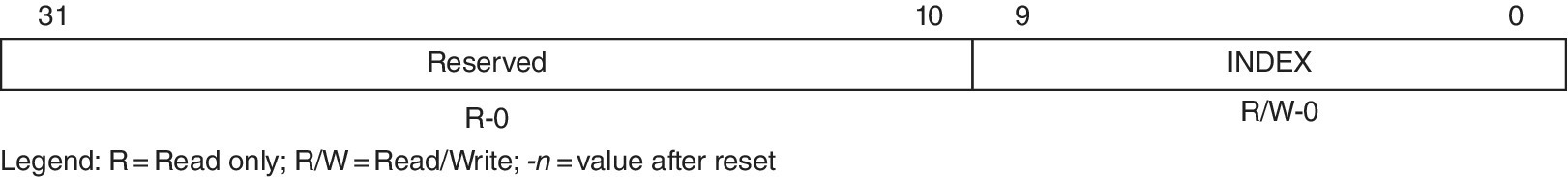
Figure 6.7 System Interrupt Status Indexed Set Register (STATUS_SET_INDEX_REG).
- A channel mapper. The aim of the CICs is to combine events. This is achieved by the combiner of each CIC that groups events. Each enabled event can select a channel as follows:
Example:
This is illustrated in Figure 6.8. The event to channel mapping is made through the Channel Interrupt Map Register (CH_MAP_REGx) illustrated in Figure 6.9 and viewed using the CCS (see Figure 6.10).
- Host interrupt mapper. Each channel must be mapped to an interrupt. However, the host mapping is fixed, that is:
- Channel 0 is mapped to Interrupt 0.
- Channel 1 is mapped to Interrupt 1.
- Channel 2 is mapped to Interrupt 2 and so on.

Figure 6.8 Example of channel mapping.

Figure 6.9 Default mapping.
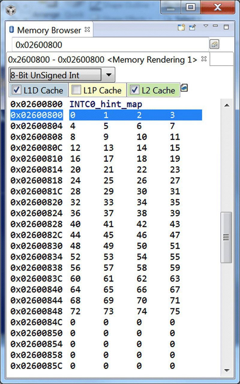
Figure 6.10 Host interrupt mapping for the CIC0 viewed with the CCS.
The channel number will depend on the device used. Each channel has a register. The mapping of the channels to host interrupts is fixed (one‐to‐one mapping). Each of the four channels has a register to define their host interrupts, and the register is read‐only; see Figure 6.11.
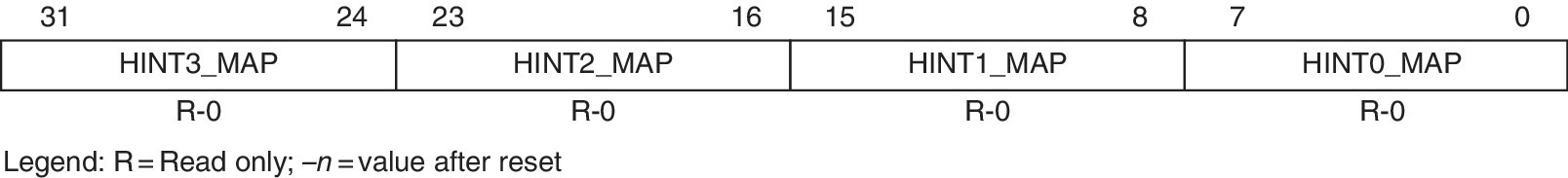
Figure 6.11 Host Interrupt Map Registers [3].
6.2 The interrupt controller
The INTC, shown in Figure 6.3 and detailed in Figure 6.16, is composed of:
- Event combiner. As its name suggests, the combiner combines many events to produce one event. There are four groups of events that can be combined (see Figure 6.17). Notice that events cannot be grouped randomly. As an example, enabled events within one group can be combined as shown in Figure 6.12 or by using the graphical configuration shown in Figure 6.13 to Figure 6.15.
- Interrupt selector. This selects up to 12 events among the 128 input events and maps them to INT[15:4] as shown in Figure 6.16. The code example above shows that Group 2 is selected to link to INT[6] (see Figure 6.14).
- Exception combiner. This combines all events and the RESET to generate a single hardware exception (EXCEP).
- IDROP mask. If the DSP receives an interrupt while the interrupt flag is still set, then an event is generated. This event is the EVT96.

Figure 6.12 Configuration script.
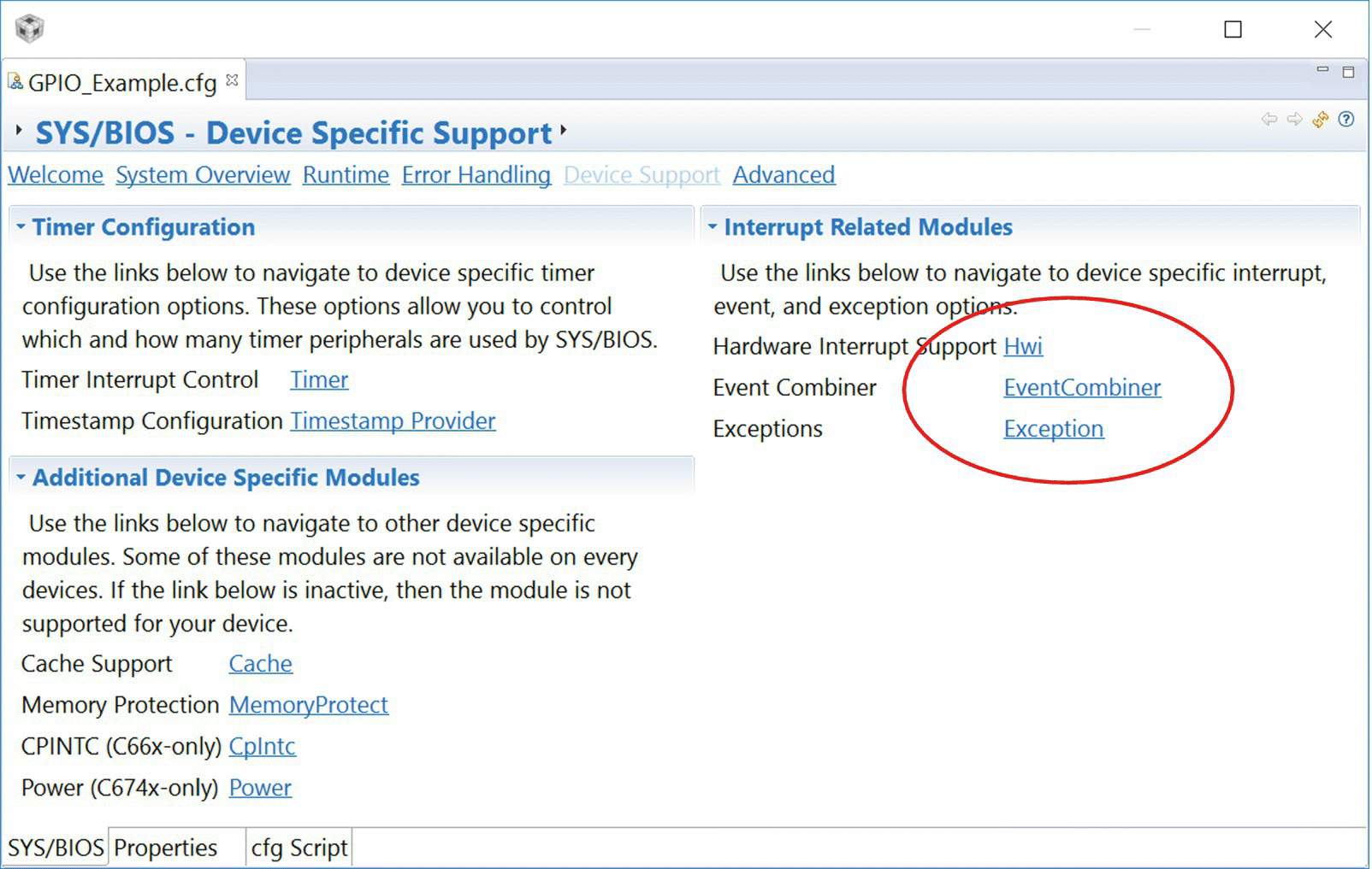
Figure 6.13 Accessing the event combiner.
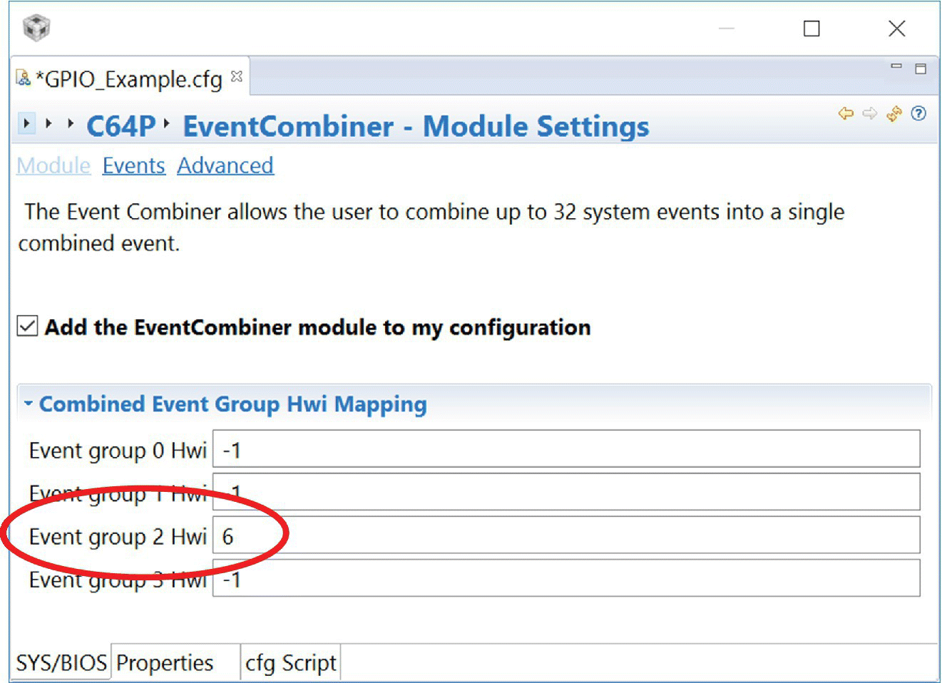
Figure 6.14 Selecting Group 2 to generate Interrupt 6.

Figure 6.15 Enabling Events 89 and 90.
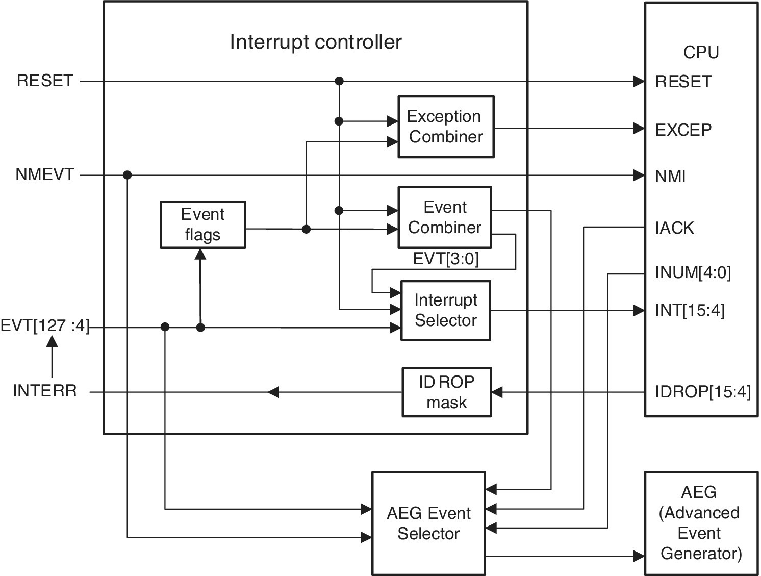
Figure 6.16 Interrupt controller.

Figure 6.17 Event combiner.
The complete interrupt system is illustrated in Figure 6.18, with the highlighted System Event 4 (SE4) being programmed to generate Interrupt 15 (INT15).

Figure 6.18 Overall functionality of the interrupt mechanism.
6.3 Laboratory experiment
There are two experiments: using the GIPIOs to trigger some functions, and using the console to trigger an interrupt.
6.3.1 Experiment 1: Using the GIPIOs to trigger some functions
- Project location: Chapter_6_CodeInterrupts_with_GPIO_Example
- Project name: Interrupts_with_GPIO_Example.
In this example, two general‐purpose input–output (GPIO) events (GPIO 14 and GPIO15) are made to generate two different functions when triggered and combined to generate one function if either event is generated (see Figure 6.19). To avoid sending real signals to the GPIOs, the events are triggered by software.
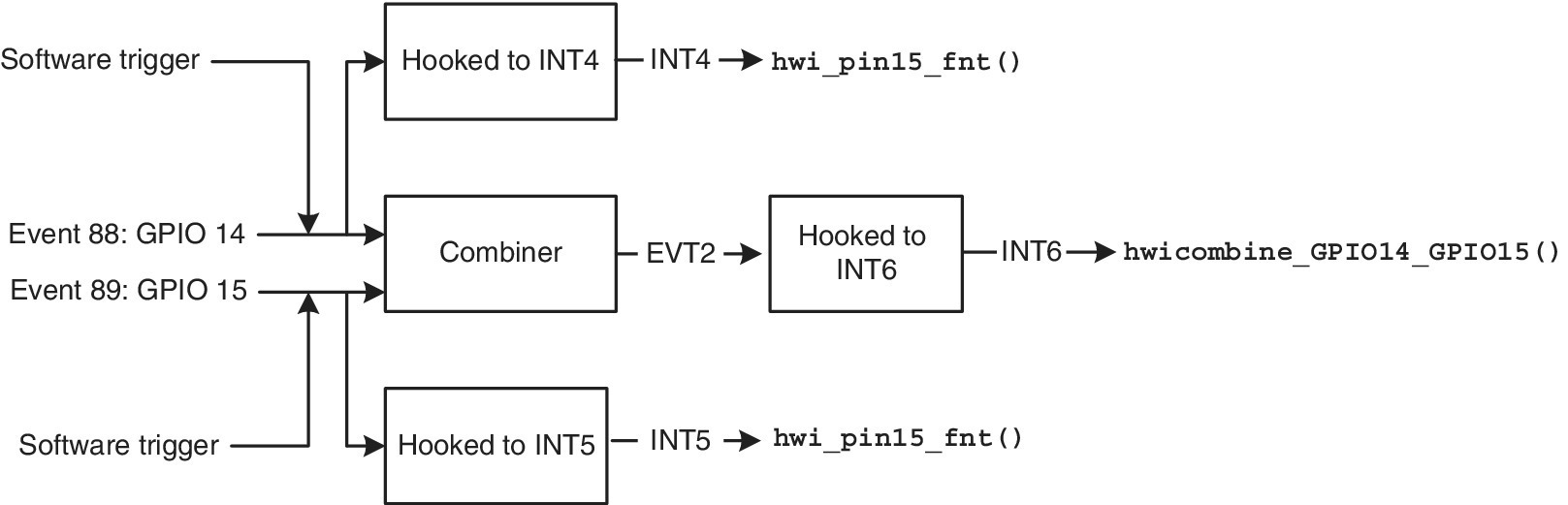
Figure 6.19 Experimental setup.
Examine the code, then compile, build and run it.
6.3.2 Experiment 2: Using the console to trigger an interrupt
- Project file location: Chapter_6_CodeCIC
- Project name: GPIO_with_CIC.
In this experiment, the application written will scan the input from the console (the user inputs a GPIO number) and call the applicate function (each GPIO triggers a different function; only GPIO0 and GPIO8 to GPIO15 are used in this example). It is worth noting at this stage that GPIOn will only trigger Core n, where n is 0 to 7; that is, GPIO0 triggers only Core 0, GPIO1 triggers only Core 1 and so on. However, GPIOx (x = 8–15) will trigger all cores.
The steps to implement this example are as follows:
- Step 1. Select an event (e.g. Event 4: EDMA3CC1 TC2 error interrupt). Later, this event will be triggered manually.
- Step 2. Map this event to one of the 1024 channels. Each interrupt is linked to one interrupt controller output of the CICx, and each of these outputs has an event ID. To map Event 4 to Channel 0 (see GPIO_Example.cfg), use:
- Step 3. Use the combiner to connect the event ID to one of the combined events (EVT[0], EVT[1], EVT[2] or EVT[3]). Since Channel 0 was used and is connected to CIC0_OUT0 which is represented by Event ID 102 (see SPUR691), therefore EVT [3] will be used.
To program this, use:
- Step 4. Now EVT[3] has to be mapped to one of the CPU interrupts (INT[15:0]). For example, if one desires to map EVT[3] to INT[15], the following code can be used:
- Step 5. Now interrupt INT15 needs to be hooked to a function. This can be achieved by the following code: where CIC_evt is the interrupt service routine.
- Step 6. After completing the setup, the event has to be enabled. This is accomplished by the following code:
- Step 7. In order to run this example, an event can be set by software. To do so, one needs to identify the interrupt status index register address to set the corresponding status of the system interrupt as shown in Section 6.1.1.
- Step 8. Open, build and load the project.
- Step 9. Group all cores so that they will all run at the same time.
- Step 10. Run all cores.
- Step 11. Enter 0 (followed by any letter) to simulate a GPIO0 signal. Enter 1 (followed by any letter) to simulate a GPIO1 signal (this has not been programmed, and therefore no output function call is performed). Enter 14 (followed by any letter) to simulate GPIO14 (followed by any letter) to simulate GPIO14 and so on. See output in Figure 6.20.
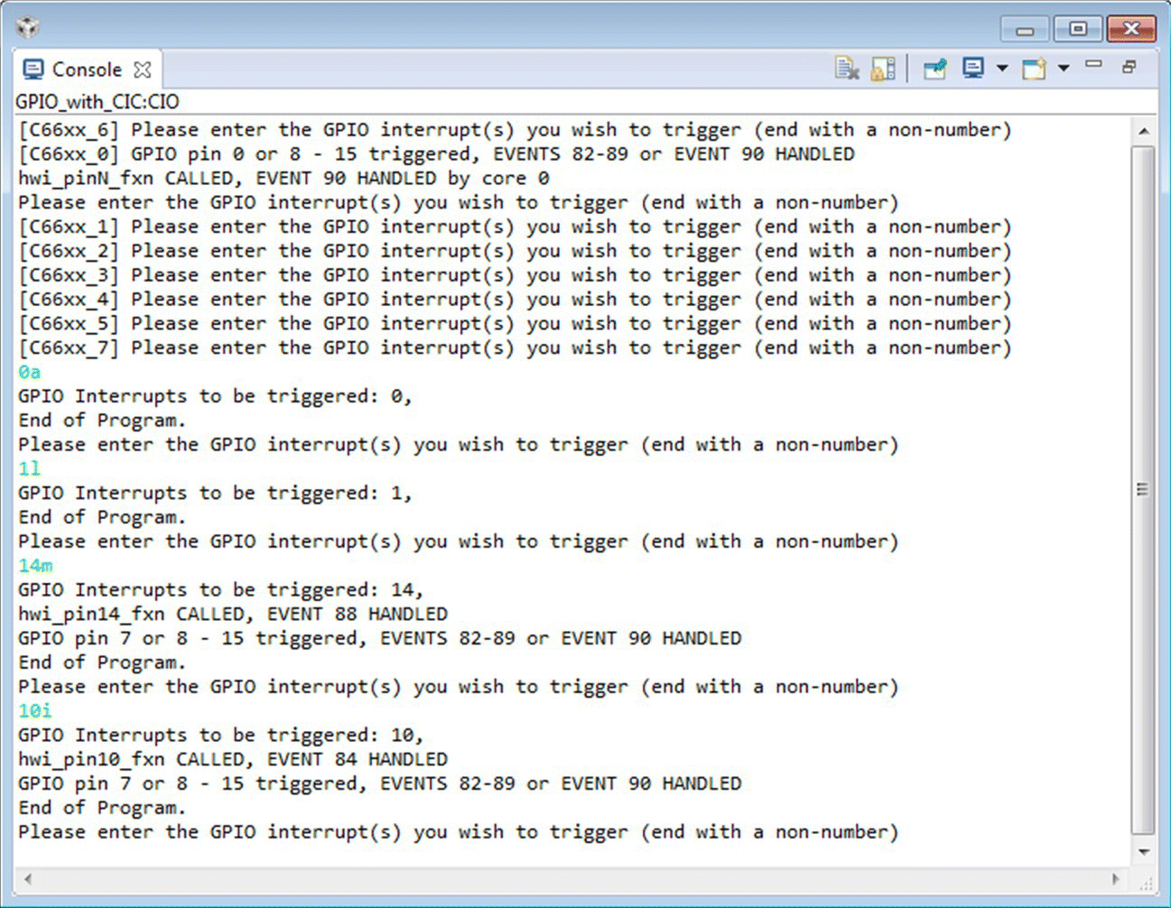
Figure 6.20 Console output showing the functions called.
6.4 Conclusion
This chapter shows how the interrupt controller events and the CIC work, and how to program them to respond to events. The examples given use the GPIO pins to provide the interrupts. To avoid sending real signals to the GPIOs, the interrupts have been set by software.
References
- 1 Texas Instruments, Multicore fixed and floating‐point digital signal processor: SPRS691E, November 2010, revised March 2014. [Online]. Available: http://www.ti.com/lit/ds/symlink/tms320c6678.pdf. [Accessed 2016].
- 2 Texas Instruments, Multicore DSP+ARM KeyStone II System‐on‐Chip (SoC): SPRS866E, November 2012, revised November 2013. [Online]. Available: http://www.ti.com/lit/ds/symlink/66ak2h12.pdf. [Accessed 11 December 2016].
- 3 Texas Instruments, KeyStone Architecture literature number: SPRUGW4A March 2012, March 2012. [Online]. Available: http://www.ti.com/lit/ug/sprugw4a/sprugw4a.pdf. [Accessed 11 December 2016].