
Message in a Bottle – Valve technology
What is ‘valve sound’?
Currently worldwide business in valves is an estimated several million dollars a year, most of which is in audio. But why have valves made a comeback? Many believe that digital music production and recording has a certain ‘sterility’ and the incorporation of valve circuitry in the recording chain assists in reducing this undesirable characteristic. Certainly, peculiarities of valve equipment and circuitry may influence the tone of the reproduced sound but it is necessary to observe the distinction, made in Chapter 2, concerning the differences between musical and recording/reproduction electronic systems. Put bluntly, and despite widespread popular belief to the contrary, it is extremely unlikely that valves magically reveal details in the music obscured by mysterious and hitherto undiscovered distortion mechanisms inherent in solid-state electronics. However, what may be said with certainty, falling as it does squarely within the remit of electrotechnical science, is that valves do exhibit a number of characteristics which may perhaps (under certain auspicious circumstances) perform better than poorly designed semiconductor equipment or in a manner which beautifies or glamorises the reproduced sound.
Harmonic distortion
The first, and most obvious, peculiarity of valve circuitry is its inherent non-linearity. In applications such as amplifiers for electric instruments this almost certainly counts as a benefit; adding richness and brightness to the perceived tone. A simple triode amplifier has a curved transfer characteristic, like that illustrated in Figure 4.1.
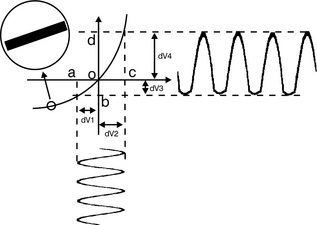
A transfer characteristic is the term given to a graph which details the relationship of voltage input to voltage output. Typically the X axis represents the input and the Y axis represents the output. So, referring to Figure 4.1 a particular voltage a at the input results in another voltage b at the output of the electronic device or circuit. Similarly, the input voltage c results in the output voltage d. Crucially, observe that in the case of the triode stage, the ratio dV1/dV2, is not the same as the ratio dV3/dV4. This is the formal definition of amplitude related distortion in all electronic systems and the figure illustrates the effect the non-linearity has on a sine-wave input waveform.
The triode’s transfer characteristic leads to the production of a set of even-numbered harmonics of rapidly diminishing strength; a fair degree of second harmonic, a small amount of fourth, a tiny amount of eighth and so on. Remember from Fourier’s findings, it is the presence of these new harmonics which account for the change in the waveform as shown in Figure 2.2. Referring to Figure 2.7 in Chapter 2, even-numbered harmonics are all consonant. The effect of the triode is therefore ‘benign’ musically.
The pentode on the other hand has a transfer characteristic in which the predominantly linear characteristic terminates abruptly in a non-linear region. This difference does not account for the preference for triodes in high quality amplification (where they are chosen for their lower noise characteristics) but may account for guitarists’ preference for triodes in pre-amplifier stages of guitar amplifiers where the triode’s rather slower transition into overload enables a player to exploit a wider range of sonic and expressive possibilities in the timbral changes elicited from delicate to forceful plectrum technique.
While harmonic distortion may have certain special benefits in musical applications, it is unlikely that non-linearity accounts for the preference for valves in recording and reproduction (monitoring or hi-fi) applications. Non-linear distortion of complex waveforms results in the production of a plethora of inharmonic distortion components known as intermodulation distortion which, without exception, sounds unpleasant, adding ‘muddle’ to the overall sound.
Intermodulation distortion
Intermodulation distortion comes about due to the presence of non-linearities in an electronic system as well.1 Take for instance the triode transfer characteristic illustrated in Figure 4.1. This characteristic is curved which, to the mathematically minded of you, will immediately imply a power law. In simple terms, a power law is a relationship which does not relate one set of values (the input voltage) to another (the output voltage) by a constant, which would yield a straight-line relationship – and incidentally a distortionless amplifier, but by a function which is made up of both constant and multiplication factor which is related to itself. Put a different way, not this:
where Eo is output voltage and Ei is input voltage
Now the crucial concept here is multiplication. The power term p in the above expression illustrates that Ei is multiplied by a version of itself and, we know from Chapter 2, that when two sine-waves are multiplied together it results in sum and difference frequencies. The two frequencies are termed to intermodulate with one another. If we imagine connecting an input signal consisting of two sine-waves to an amplifier with such a characteristic, the result will betray the generation of extra tones at the sum frequency (sin A + sin B) and at the difference frequency (sin A – sin B). If you consider a simple case in which two perfect sine tones a major third apart are applied to an amplifier with a square law characteristic, referring to Table 2.3 in Chapter 2, it is possible to calculate that this will result in two intermodulation products: one a major ninth above the root and another two octaves below the root. This results in the chord in Figure 4.2. Now imagine this effect on every note within a musical sound and the interaction with every overtone with every tone and overtone within that sound and it is relatively obvious that distortion is an unlikely suspect in the hunt for the sonic blessings introduced by valve equipment.
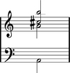
Figure 4.2
Headroom
One benefit which valve equipment typically does offer in high-quality applications is enormous headroom. This may explain their resurgence in microphone pre-amplifier designs which must allow for possibly very high acoustic energies – for instance when close-miking a loud singer or saxophonist – despite the technical problems involved in so doing (see Figure 4.3 in which a quite beautiful modern microphone due to Sony incorporates valves for the signal path and semiconductor technology in the form of Peltier heat-pump technology to keep the unit cool and secure a low-noise performance). Technically valve microphone amplifiers have a great deal in common with the phono pre-amplifier illustrated in Figure 4.10 later in the chapter. (Indeed the justification for that valve design lay in its ability to handle the large peak signals.) But even in this instance the ‘benefits’ which valves bestow are a case of ‘every cloud having a silver lining’ because valves are only able to handle signals with very high peaks because they display significant non-linearity. Figure 4.1 illustrates this too, in the magnified portion of the curved transfer characteristic of a triode amplifier. The magnified section approximates to a straight line, the characteristic required for accurate and distortion-free operation. It illustrates that, in order to obtain a linear performance from a valve, it is necessary to operate it over a very small portion of its overall transfer characteristic, thereby providing (almost by default) an immense overload margin.

Interaction with loudspeakers
A characteristic of all valve power amplifiers (high quality and instrumental types) is the lower degree of negative feedback employed. Especially when compared with solid-state designs. Instrumental amplifiers, in particular, often opt for very little overall feedback or none at all. Because the signal in a valve amplifier issues from the high impedance anode (or plate) circuit, even the action of the power output-transformer2 cannot prevent valve amplifiers from having a relatively high output impedance. This produces, via an interaction with the mechanism of the loudspeaker, a number of pleasant sonic characteristics that certainly profit the instrumental musician and may elicit a euphonious and pleasant (if far from accurate) response in a high quality situation.
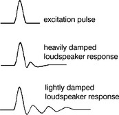
It was noted in the last chapter that moving coil microphones and loudspeakers worked according to the same principles applied reciprocally. So that inside a microphone, a coil of wire produces a small electric current when caused to move within a magnetic field by the force of sound waves upon it. Whereas in a loudspeaker sound waves are generated by the excitation of a diaphragm connected to a coil of wire in a magnetic field when an audio signal passes through the coil. It should therefore come as no surprise to discover that a loudspeaker, excited into motion, generates a voltage across the driver coil. It is one of the functions of a perfect power amplifier that it absorb this voltage (known as a back-EMF). If the amplifier does this duty, it causes the current due to back-EMF to recirculate within the coil and this damps any subsequent movements the coil may try to make. A valve amplifier, on the other hand, especially one with a small degree of negative feedback, has a relatively high output impedance and therefore fails to damp the natural movement of a loudspeaker following a brief excitation pulse. This effect is illustrated in Figure 4.4. Because the natural movement of the loudspeaker is invariably at its resonant frequency – and this is always pretty low – the perceived effect of insufficient damping is of more bass, albeit of a rather ‘tuneless’ kind! In small rooms, which cannot support bass frequencies, and with small loudspeakers this effect can lead to an artificially inflated bass response which may suit some individuals.
Reduction in loudspeaker distortion
Another consequence of the high output impedance of a valve amplifier, and one that may be the nearest phenomenon yet to a mysterious semiconductor distortion mechanism, is the reduction in mid-range loudspeaker amplitude distortion. This is due to uncoupling the dependence of cone velocity on the changes in the magnetic circuit and lumped electrical impedance. In the relationship of cone velocity to amplifier output voltage, these terms (which are themselves determined by the position of the cone) are present. They are not in the relationship which relates amplifier output current to cone velocity. The relatively high output impedance of valve amplifiers thereby has some advantages in securing a reduction in harmonic and intermodulation distortion.
Valve theory
I suppose electronic musicians and sound engineers might claim Thomas Alva Edison as their profane ‘patron saint’. But that wouldn’t be justified because Edison, who was probably the greatest inventor in history, changed the lives of ordinary people in so many ways that to claim him for our own would be to miss his other achievements. Among them electric light, the modern telephone, the typewriter, the motion picture as well as the father of modern industrial research! Nevertheless Edison did overlook patenting the electronic diode and thereby failed to reap the benefits of the first electronic, rather than electrical, invention. This fact is all the more amazing in that in the 1880s, he experimented with a two-terminal vacuum tube formed by putting an extra plate in the top of a light bulb; the filament acting as a cathode and the plate as an anode. (In America, the anode is still referred to as the plate.) Edison made the far-reaching observation that, in such an arrangement, conventional-current travelled in one direction only; towards the cathode. However, and perhaps because no mechanism had yet been advanced for why such an effect should occur (the electron was not discovered until 1899), Edison failed to see what application such an effect might have.
Invention of the diode
It is said that Edison never forgave himself for overlooking what, in 1904, J.A. Flemming had the vision to see; that the phenomenon which he had observed had commercial application in the detection of wireless waves. Braced with the discovery, by J.J. Thompson in 1899, of the electron, Flemming saw the potentialities (drawing on a hydraulic or pneumatic analogy) of an ‘electronic valve’ which allowed current to be passed in one direction while prohibiting its flow in the other. He realised that this ‘valve’ had applications in early wireless, where experimenters had been striving to discover something which would react to the minute alternating potentials produced in a receiver of wireless waves. Flemming’s valve, by passing current in one direction only, produced a DC output from a radio frequency AC input, thereby acting as an ‘indicator’ of radio waves, what we today would call a detector.
Invention of the triode
In 1907, Dr Lee de Forest took out a patent in America for a valve like Flemming’s, but with a third electrode, consisting of a mesh of wires interposed between the anode and the cathode. De Forest noticed that the potential of this grid exercised a remarkably strong control over the anode current and, moreover, saw that such a phenomenon increased enormously the potentialities of the valve because it could act as a detector and, most crucially, as an amplifier, and ultimately as a generator of oscillations – or an oscillator. So how exactly does the triode valve work?
Thermionic emission and the theory of electronic valves
The modern thermionic triode valve is a three-electrode amplifying device similar – in function at least – to the transistor (see Figure 4.5).
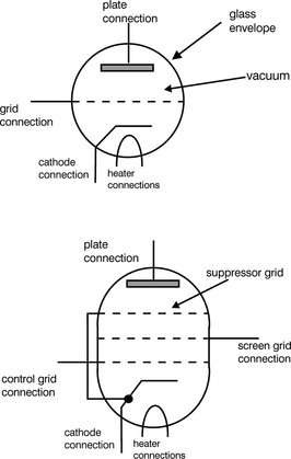
Externally the valve consists of a glass envelope in which the air has been evacuated. Each electrode is formed of a metal – each a good conductor of electricity. In an electrical conductor all the free electrons move about at random. When the valve is energised, one of the electrodes – the cathode – is heated (by means of a dedicated heater element which must have its own supply of electricity) to a point that this random motion of the electrons is sufficiently violent for some of them to leave the surface of the metal altogether. This phenomenon is known as thermionic emission. If there is no external field acting on these escaped electrons they fall back into the cathode. If another electrode within the valve is connected to a positive potential, the electrons on leaving the cathode will not fall back but will accelerate off towards the other electrode. This other electrode is called the anode. The passage of electrons from cathode to anode establishes a current which passes between these two electrodes. (Of course, convention has it that the current flows the other way, from anode to cathode.) The function of the third electrode, the grid (which is manufactured literally – just as it was in de Forest’s prototype – as a wire grid, very close to the cathode), is to control the magnitude of the stream of electrons from cathode to anode. This is achieved by varying a control voltage on the grid, so that when its potential is appreciably more negative than the cathode, the electrons – leaving by thermionic emission – are repelled and are thwarted in their usual passage towards the anode and no current flows through the valve. And when, instead, the grid is made nearly the same potential as the cathode, the electrons pass unhindered through the grid and reach the anode, as if no grid electrode was interposed at all. At values in between the current varies proportionately. Because the grid is always held negative in relation to the cathode no current flows in this control circuit (unlike the transistor but more like the FET) so a very feeble control voltage can be made to control a much larger current – the essence of any amplifying stage.
Characteristic curves
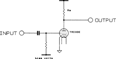
If we plot the anode current through a triode valve at various anode voltages and grid voltages we obtain a family of curves like those illustrated in Figure 4.6. These are termed characteristic curves. Note that each curve relates to the relationship of anode current to anode volts for a particular grid voltage; in this case for a particular triode valve code numbered 12AU7. Notice also that each curve is relatively straight except near the axis where it bends. Now look at the line drawn with an opposing slope to the valve curves. This is called a load-line and it represents the current/voltage relationship of a resistor Ra (the load) so arranged in circuit with the valve as shown in Figure 4.7. Observe that when the anode voltage is zero, all the current flows through Ra, and – if the anode voltage is equivalent to the rail volts – no current flows through Ra: hence the opposing slope. Because the supply rails for valve circuitry are very much higher than those associated with transistor circuitry, the rail supply is often referred to as an HT (high tension) supply.
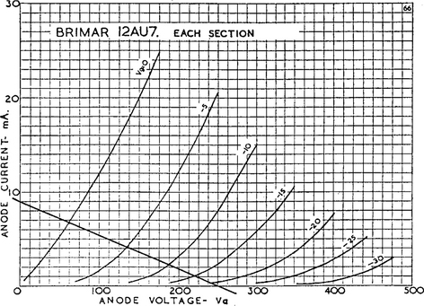
In fact, Figure 4.7 is a simple valve amplifier and we can now calculate its performance. By reading off the calculated anode voltages for grid voltages of −10 V (290 V at anode) and 0 V (60 V at anode) we can calculate that the stage gain will be:
(190 – 60)/10 = 13 times or 22 dB
This is typical of a single-stage triode amplifier and will no doubt seem pitifully small for those brought up on transistor circuitry. One important point to note when inspecting the curves of Figure 4.6 – try to imagine changing the slope of the load-line. You will see that it has very little effect on the stage gain; once again an unusual phenomenon if you are used to solid-state circuits. This is because the triode valve has a low anode impedance and the mechanism is more clearly understood by considering the equivalent circuit of a triode amplifier which is illustrated in Figure 4.8 and is, effectively, Figure 4.7 redrawn. (Remember that in signal terms, the load is returned to the cathode end of the valve via the very low PSU impedance.) As you can see, the anode impedance (or resistance ra) is in parallel with the load resistor and so swamps the higher value load resistor. The stage gain is defined by gm (mutual conductance which is a constant and is dependent upon the design of the particular valve) times the load (Ra) in parallel with the internal anode resistance (ra). Note that the internal current generator has the dimension (–gm.eg) where eg is the grid potential.
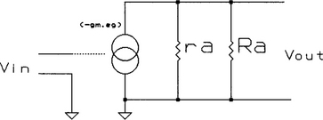
The input impedance at the grid is effectively infinite at DC but is gradually dominated at very high frequencies by the physical capacitance between the anode and the grid. Not simply because the capacitance exists but because (as in solid-state circuitry) this capacitance (sometimes referred to as Miller capacitance) is multiplied by the stage gain. Why? Because the anode voltage is in opposite phase to the input signal (note the minus sign in the stage gain formula) so the capacitance is effectively ‘bootstrapped’ by the action of the valve itself.
Development of the pentode and beam tetrode
It was this troublesome Miller capacitance (especially in radio work, where high frequencies are employed) that led to the invention of the tetrode valve, in which was interposed another grid at a fixed positive potential between the grid and the anode. This extra (screen) grid being held at a potential at, or near to, the value of the supply rails thereby neutralising the Miller capacitance by screening the effect of the anode upon the control grid. Unfortunately, the simple tetrode, while successful in this respect (the second grid reduced the effect of the Miller capacitance to about one-hundredth of the value in a triode!) has the very great disadvantage that the electrons, when they reach the anode, dislodge extra electrons; an effect called secondary emission. In a triode these extra electrons are ‘mopped up’ by the anode so nobody is any the worse for it. But in a simple tetrode, especially when the anode volts fall below the screen-grid volts, it is the screen grid which attracts these secondary electrons and they are thus wasted. In practical tetrodes, steps must be taken to prevent this effect and this is achieved by forming the grids, and indeed the entire valve, so that the electrons flow in beams through both structures, the resulting valve being known as a beam-tetrode. All modern tetrodes are beam-tetrodes. The alternative solution is to install yet another grid between the screen grid and the anode called the suppressor grid, which is kept at the same potential as the cathode and which is often connected internally. This brings the total number of internal electrodes to five and the valve is therefore known as a pentode. The zero (or very low) positive potential of the suppressor grid has the effect of turning the secondary electrons back towards the anode so that they are not lost.
The addition of the extra grid, in the case of the tetrode (or grids, in the case of the pentode), although primarily to extend the frequency range of a valve way beyond the audio range, has a remarkable intensifying effect on the performance of a valve. It is this enhancement and not their superior RF performance which ensures their use in audio applications.
What is the nature of this enhancement? Well, the equivalent circuit shown in Figure 4.8 is equally valid for a pentode but the value of ra, instead of the 5k to 10k in a small triode, is now several megohms. The stage gain is thereby radically improved. Typically a small pentode valve will have a stage gain of 100 times (40 dB), ten times better than a triode stage. Audio output valves are often either pentode or beam-tetrode types.
Valve coefficients
The maximum voltage amplification which a valve is capable of, given ideal conditions, is called the amplification factor; generally designated with the Greek letter μ. This is not truly constant under all conditions (except for a theoretically ideal valve) and varies slightly with grid bias and anode voltage.
Technically μ is defined as follows: expressed as a ratio, the incremental change in plate voltage to the incremental change in control-grid voltage in the opposite direction – under the conditions that the anode current remains unchanged (i.e. with a current source for an anode load) and all other electrode voltages are maintained constant. So:
The two other principal valve coefficients, mutual conductance and anode resistance, we have met already. However, although we treated them earlier as constants, both coefficients are dependent to some extent on applied electrode voltages. Mutual conductance (gm) is defined thus:
That is, the change in anode current, for a given change in grid voltage, all other voltages remaining the same. Anode resistance (ra) is defined as:
There is an exact relationship between these three principal valve coefficients, provided they have all been measured at the same operating point:
Sometimes you will read, especially in older literature, references to reciprocals of these coefficients. For completeness these are defined below:
Practical valve circuits
The graphical technique explained in the last section is worthwhile in that it gives an intuitive feel for the design of valve circuits. It is, however, rather cumbersome and is not usually required for the majority of simple design tasks. Moreover it leaves several questions unanswered, such as the optimum bias conditions etc. For this, and virtually everything else the practical designer needs to know, all that is usually required is the manufacturer’s data. Let’s take as an example the 12AU7 valve (ECC82) which we met in the previous section. Using graphical techniques, we were able to ascertain that the stage gain of this particular triode valve circuit would be about 13 times, or 22 dB. We’ve already noted that the stage gain of a triode valve amplifier depends only very little on the value of anode resistor. This phenomenon, which we might term the ‘device-dependent’ nature of valve design, is certainly not consistent with most readers’ experience of transistor stages and may take some getting used to for modern engineers. This consistency in performance makes it possible to tabulate recommended operating conditions for a valve in a manner that would be quite impossible for individual transistors. Usually, the manufacturers state a number of different recommended operating scenarios. Data for the 12AU7 (ECC82) valve consist of the following:
Operation as a resistance coupled amplifier

The circuit illustrated in Figure 4.9 is derived from the tabulated conditions. Note the addition of several extra components. First, the inclusion of a resistor in the cathode circuit. Second, the addition of the 1 meg grid bias resistor and input coupling capacitor Cin. Valves are virtually always biased as shown, with a positive potential being derived at the cathode (by means of a series resistor through which the anode current flows) and the grid returned to ground via a very high value resistor. This latter resistor is absolutely necessary, for although a valve takes only a minute bias current via its grid circuit, it does take some and this resistor is included to provide such a current path. The advantage of this biasing scheme, known as cathode biasing, is inherent stability. If the current through the valve starts to rise, the potential at the cathode increases with respect to the grid, and so the grid bias moves more negative, thereby reducing the anode current. The only disadvantage of this scheme in a practical amplifier is the generation if a signal voltage in phase with the anode current (and thus out of phase with the grid signal voltage) due to the varying grid current in the cathode bias resistor. If the resistor is left unbypassed, it generates a negative feedback signal which raises the output impedance of the stage and lowers stage gain. Hence the third inclusion; the large value capacitor placed across the cathode resistor to bypass all audio signals to ground at the cathode circuit node.
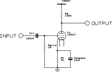
The value of Cin is chosen so that the low-frequency break point is below the audio band. Curiously enough, this network and the impedance of the anode supply are related: one of the common problems encountered with valve amplification is low-frequency oscillation. Almost certainly a surprise to engineers weaned on transistor and op-amp circuitry, this results from the predominance of AC coupled stages in valve equipment. Just as high-frequency breakpoints can cause very high-frequency (supersonic) instability in transistor equipment, wherein phase lag due to several networks causes the phase shift through the amplifier to equal 180° when the gain is still greater than 1; phase lead – due to the high-pass filtering effects of several AC coupled stages – can cause instability at very low (subsonic) frequencies in valve circuits. The audible effects of this type of instability are alarming, producing a low-frequency burble or pulse. In fact a sound which is admirably described by its vernacular term – motor-boating! Low-frequency oscillation typically results from feedback signal propagation via the power supply which (as a result of the elevated voltages in valve equipment) may not be as low an impedance as is typical in solid-state equipment. In order to prevent this, valve equipment designers typically decouple each stage separately. Now, let’s look at some practical valve amplifiers so as to apply our knowledge of valve circuitry.
A valve preamplifier
Figure 4.10 shows a design for a vinyl disc pre-amplifier that I designed and which ran for some years in my own hi-fi system (Brice 1985). It is a slightly unusual design in that it incorporates no overall negative feedback, passive RIAA equalisation and employs a cascode input stage.
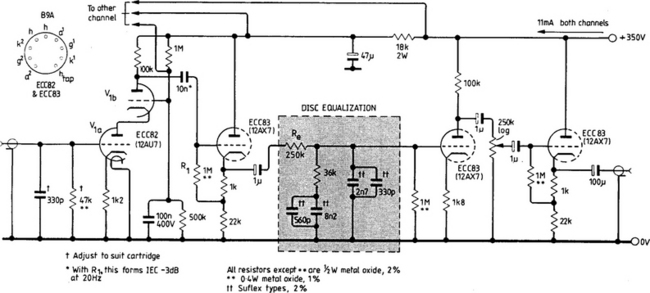
In transistor equipment, the problem with passive equalisation is the risk of overloading the first (necessarily high-gain) stage due to high-level treble signals. With valves this does not present a problem because of the enormous headroom when using a power supply of several hundred volts. The usual choice for a high-gain valve stage is a pentode but these valves generate more shot noise than triodes because of the action of the cathode current as it splits between the anode and screen. Instead I used a cascode circuit. Like so many other valve circuits this has its origins in radio. Its characteristics are such that the total stage noise is substantially that of triode V1a. But the gain is roughly the product of the anode load of V1b and the working mutual conductance of V1a. In other words it works like a pentode but with lower noise!
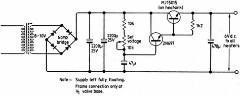
The RIAA equalisation is shown in a dotted box. This is to dissociate myself from this section of the circuit. If you have your own ideas about RIAA equalisation then you can substitute your own solution for mine! On a general note, I disagree with those who say there is no place for valves in low-level circuitry. Well designed valve circuitry can give superlative results. Hum can sometimes be a problem. In this design I left nothing to chance and powered the valve heaters from a DC regulated power supply (Figure 4.11). The HT was also shunt stabilised using cold-cathode glow-discharge tubes. The power supplies were built on a separate chassis. The more common ECC83 valve would be suitable as the first stage cascode valve except that the ECC82 is more robust in construction and therefore less microphonic. I have found, from bitter experience, that there is no alternative but to select low-noise valves individually for the first stage valve.
Power amplifier
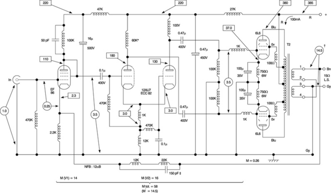
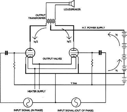
Figure 4.12 is a circuit diagram of a practical 20 watt Class-A beam-tetrode amplifier. This amplifier utilises a balanced (or push-pull) output stage employing two 6L6 beam tetrode valves. This is the most common form of audio amplifier configuration. Why? The answer is balance. As with so many other practical engineering solutions the lure of symmetry and equilibrium triumph in the human mind. In Figures 4.13 and 4.14 a single-ended and balanced (push-pull) output stage are drawn for comparison. The balanced version has a number of important advantages over its single-ended cousin.

Magnetisation of the output transformer
All but a very few special valve amplifiers employ an output transformer. This component can be thought of as an electrical gearbox coupling the high impedance valve outputs to the low impedance loudspeaker. Transformers work using the principle of electromagnetism which you may remember investigating in school physics where you may have proved it was possible to create an electromagnet by winding wire around an iron (or steel) nail and passing current through the wire. Had it been possible in that school experiment to control the current through the magnet and measure the power of the magnet and how it related to current (perhaps by the number of paper-clips it could pick up) you would have found a linear relationship up to a certain point; the number of paper-clips would be directly proportional to current, up to a certain value of current. After that value of current had been reached, however, the magnet would not pick up any more paper-clips no matter how much more the current was increased. It would simply serve to warm up the magnet. This effect is known as magnetic saturation (and we will meet it again in relation to magnetic tape). It is due to all the magnetic domains within the nail eventually being used up. After that point the nail simply cannot become more magnetised. Exactly the same limitation exists with output transformers. The process (as within all transformers of converting electricity into magnetism and back again) is distortion free, so long as the transformer core does not become saturated. When that begins to happen, the process becomes non-linear and audible distortion will start to be produced.
If you compare Figures 4.13 and 4.14, you will notice, in the case of the single-ended output stage, that a continuous standing or quiescent current (Iq), flows from the power supply, through the transformer and valve and back to the power supply. Because audio signals are assumed (for design purposes at least) to be symmetrical, this standing current must equal half the maximum that the output valve is designed to carry. A typical amplifier with 10 watts output would require a standing anode current of about 70 mA. This much current would produce a magnetic core flux density of perhaps 5000 to 6000 gauss.
Now consider Figure 4.14. Here the quiescent current flows from the power supply into the centre of the output transformer. From here, it splits – half in one direction into one output valve and half in the other direction into the other output valve. The current, once shared between the valves, recombines in the common cathode circuit and flows back to the power supply. The great advantage of this configuration is that, because the current flows in at the middle of the transformer winding and away in opposite directions, the magnetic effects within the core of the transformer cancel out and there is thus no quiescent magnetisation of the core in a balanced stage.
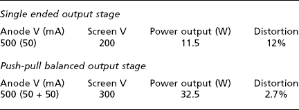
Reduction in distortion products
It is a widely (and incorrectly) held belief that valves are inherently more linear than transistors. This is absolutely not the case. The transistor is a remarkably linear current amplifier. On the other hand, the valve is a relatively non-linear voltage amplifier! For example, a 6L6 output valve used in a single-ended configuration like that shown schematically in Figure 4.13 will produce something in the region of 12% total harmonic distortion at rated output. But the balanced circuit has an inherent ability to reduce distortion products by virtue of its reciprocity in a very elegant way. Essentially each valve produces an audio signal which is in opposite phase at each anode. (For this to happen they must be fed with a source of phase-opposing signals; the role of the phase-splitter stage which will be considered below.) But their distortion products will be in-phase, since these are dependent upon the valves themselves. So these distortion products, like the transformer magnetisation, will cancel in the output transformer! This is empirically borne out: Table 4.1 annotates my own measurements on an 807 beam-tetrode amplifier used in single and balanced configuration. The numbers speak for themselves.
Returning to the complete amplifier pictured in Figure 4.12. Note that the first stage illustrates a practical pentode amplifier; the supply to the screen grid of V1 via R4 (2M2). This must be decoupled as shown. The suppressor grid is connected internally. This is followed by the phase-splitter stage. In the amplifier illustrated, the phase splitter is known as a cathode-coupled type and is relatively familiar to most modern engineers as a differential-amplifier (long-tailed pair) stage. The signal arriving at the grid of the left hand valve is equally amplified by the two valves and appears at the two anodes in phase opposition. These signals are then arranged to feed the grids of the output valves, via coupling capacitors.
Mark the slightly different anode loads on each half of the phase splitter which are so arranged to achieve a perfect balance between circuit halves.
If Ohm’s law was really a law, there would be an awful lot of electronic components in gaol! Because there’s a whole range of important electronic components which do not obey the ‘law’. These are neither insulators, resistors or conductors. Instead they’re somewhere between all three and are hence termed semiconductors.
Semiconductors display important non-linear relationships between applied voltage and the current through them. Look at graph Figure F4.1: this is the graph of the current through a semiconductor diode at varying voltages. When a negative voltage is applied, no current flows at all: and when a positive voltage is applied, nothing much happens before the voltage reaches 0.7 V, after which the current rises very swiftly indeed.

The graph was obtained by plotting the relationship of I / V in a silicon semiconductor diode. The most important effect of the diode is its peculiarity that it allows current to flow one way only. It’s therefore useful in obtaining DC current from AC current – a process which is required in most electronic equipment in order to turn the mains supply into a DC supply for the electronics.
The significance of the positive 0.7 volts ‘twilight-zone’ in the silicon diode is due to deep quantum physics. Effectively electrons passing through the diode have to achieve a sufficient energy level to get the diode to start to conduct and for this they require a certain voltage or electro-magnetic force. This 0.7 volts is known as the diode’s offset voltage.
Transistors spring from a common technological requirement that a small controlling input may be used to manipulate a much larger source of power; just as pushing the car’s accelerator pedal (which requires very little effort) can cause you to hurtle down an autoroute at 200 k.p.h.! In the nineteen-twenties electronic valves were developed for this purpose, now these have been superseded (except in some audio equipment – see Chapter 4) by transistors which may be thought of as semiconductor valves!
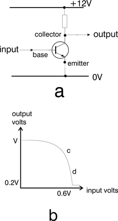
Figure F4.2 illustrates a simple transistor amplifier. The input voltage being applied at the base of the transistor and the output developed across the resistor Rload. The graph illustrates the input voltage and the output voltage at the relevant ports. Note the three terminals of the transistor which are also labelled; base, emitter and collector respectively, the input being at the base and the output at the collector. This is the most common arrangement for a transistor amplifier.
From the graph it’s pretty apparent that without qualification this doesn’t represent a very useful amplifier! It’s only over the region annotated c–d, that the transistor may be used as a linear device. For this to happen the input signal must be biased into the region close to 0.7 V (the offset voltage), and be prevented from swinging beyond the limits of this sector. Unfortunately this isn’t as simple as it sounds due to the incredibly high gain of the amplifier in this region which would involve controlling the voltage of the base within thousandths of a volt (millivolts or mV). Worse still transistors are very susceptible to changes in temperature (offset voltage is actually related directly to heat). All of which would make for a very fragile amplifier without the adoption of several important circuit techniques illustrated in Figure F4.3; which represents a practical transistor amplifier stage. Note the important addition of Rb1 and Rb2 which are so arranged to provide a constant bias voltage at the base terminal. However, you’ll note that the bias voltage chosen is not close to 0.7 volts but is instead several volts. The emitter is 0.7 V less than the voltage on the base but the remainder of the bias voltage exists across resistor Re. Notice that the signal is input to the stage via capacitor Cin. Notice also the capacitor which is placed across Re. This is a large value capacitor and effectively ensures that at audio frequencies the impedance of the emitter circuit is close to zero. However at DC, the emitter circuit is dominated by Re. This ensures that the AC gain of the amplifier stage (at all audio frequencies) is very much higher than the gain at DC. This is a very common technique in transistor equipment from simple transistor amplifiers to 1000 watt power amplifiers.

In the circuit illustrated, the collector current is set to 2.3 mA. We know this because 2.3 volts exists across Re. We can also calculate the voltage at the collector because most (all but about 1%) of the current which flows in the emitter circuit, flows in the collector circuit. In other words, the current doesn’t come from the base circuit. This is a very important point because remember the whole idea behind an amplifier is to control a much larger force by means of a small controlling force; if current flowed from the base circuit it would sap energy from the controlling circuit.
So, if 2.3 mA flows in the collector circuit through Rc, the voltage at the collector (using Ohm’s law) will be about 0.0023 × 2200 = 5.06 volts less than the power supply,
We can work out the gain at DC by imagining changing the bias voltage to 4 V (i.e. one volt more). The voltage between the base and the emitter will remain about the same (0.7 V) so in this case the emitter current will be 3.3 V/1k = 3.3 mA and the volt-drop across Rload will be 3.3 mA × 2.2 k = 7.3 V.
So a change of one volt at the base will cause 7.3 – 5 = 2.3 V change at the collector, in other words a gain of 2.3 times. Notice that this value is close to the value of Rload/Re, in fact this may be used as an approximation for all practical calculations.
The stage gain at AC of the transistor stage in Figure F4.3 is given by,
Where gm is a termed mutual conductance and is an expression which defines the degree of change in collector current for a given change in base voltage. This sounds simple except that in a transistor gm is related to collector current by the expression,
In other words, gm is not constant in a transistor but is dependent upon its operating condition. (Compare this with valves in Chapter 3.) Nevertheless, the simplification is usually made that the gm is calculated at the bias condition and this is used to predict the gain of the stage – and this works very well indeed due to the high gain of a transistor.
So, in Figure F4.2, the stage is ‘sitting in’ 2.3 mA of current (this is often termed quiescent current) so,
which implies that the collector current will change by 92 mA for every 1 V change in base voltage. This will cause a 92 mA × 2200 = 202 V swing at the collector output. Which is the same thing as saying the stage has a gain of about 200 times or 46 dB.
Of course the collector can never swing 202 V, instead it can probably swing between very close to the rail and to within about 0.2 V of its emitter volts (2.3 V), a swing of about 10 V. In this application, input voltage would have to be limited to about,
The amplifier we looked at above was designed using a NPN transistor, which has a conventional current path from collector to emitter; this is indicated by the arrow which shows the current leaving by the emitter! But there’s actually another type of transistor called a PNP type which works exactly the same way (from an external point of view – internally the physics are quite different) in which the current arrives by way of the emitter and exits by the collector. Not surprisingly, this is distinguished by an arrow which points in the opposite direction. Modern convention has it that a PNP transistor is also drawn the other way up to its NPN cousin; because it makes circuit diagrams easier to read if current always flows from the top of the page to the bottom.
The different types of transistors are very useful in building amplifier structures which would otherwise require AC coupling; as was current in valve equipment. Figure F4.4 illustrates a three stage amplifier using a PNP transistor in the second position. The circuit is said to be DC coupled and, not only does the PNP transistor allow the designer to dispense with biasing arrangements for the second and third transistor, but ensures that there is gain (and critically no phase shift) at low frequencies. This enables the amplifier to be used in all sorts of roles which would be unsuitable for the AC coupled, valve amplifier.
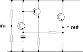
In fact the little amplifier in Figure F4.4 is so good that it can be used for a wide variety of varying operations. It is therefore termed an operational amplifier or op-amp for short. Fact Sheet #7 explains some of the roles for an op-amp.
1In fact harmonic distortion is really only a special type of intermodulation distortion.
2The anode circuit of a valve is, in many ways, similar to the collector circuit of a transistor (i.e. very high impedance). You can think of a valve output transformer as an electrical gearbox coupling the high impedance valve outputs to the low impedance loudspeakers. See later in chapter.