
Materials form the basic underlying building block of nearly every advanced technology, and nanotechnology is no exception. Most technologies have various levels of differentiation, which can be broken down roughly into (1) materials, (2) design and fabrication, and (3) integration. In the case of some conceptual nanotechnologies, the path to achieve the last two levels is not at all clear. However, the science and technology of nanomaterials are both vibrant fields, with breathtaking advances on a daily basis. In many ways contemporary nanoscience is essentially the study of nanomaterials.
What differentiates nanomaterials from classical materials science, chemistry, and the like is the degree of control. Whereas many scientific disciplines have for more than a century dealt with phenomena and understanding on the atomic scale, the emerging field of nanomaterials strives to achieve control on that level beyond stochastic processes. One might view this field as a variant of engineering; instead of studying what is, we try to create what never was—and now on an unprecedented level.
One of the original areas of nanoscience—the production of nanometer-scale particles of various materials—is nearly as old as human civilization. Not until the past few decades have researchers begun to appreciate the unique properties of nanoparticles. With the understanding of structure and synthesis, researchers worldwide have gained nearly atomistic control over size and properties, creating such intriguing structures as “core-shell” quantum dots. Nanoparticles are finding applications in a number of diagnostic and biomedical uses and will become widespread when toxicity and functionalization issues are solved.
The unarguable poster child of nanoscience is the carbon nanotube (CNT), which are graphene sheets rolled into a perfect cylinder with mind-bending aspect ratios, often being only a nanometer in diameter but many micrometers in length. More interestingly, their electronic structure is dramatically dependent on dimension and twist—an exciting advantage if these parameters can be controlled, but generally viewed as a limitation until these problems can be solved. Nonetheless, fascinating electrical, thermal, and structural properties of single-walled nanotubes (SWNTs) have been measured. The scaling of this understanding to large-scale synthesis and the use of these properties on a macroscopic scale remain challenges.
More recently, inorganic semiconducting nanowires have begun to attract attention as an alternative to nanotubes because their electronic properties are easier to control. First explored in the early 1990s, these single-crystal nanowhiskers, with dimensions of only tens of nanometers, have seen a resurgence in the past few years because of the development of a wide variety of synthesis methods. In addition, the range of materials that can be fabricated into nanowires is impressive, giving a large design space for property control. Although the exploration of these systems is still in its infancy, this field represents a rapidly expanding frontier of functional nanomaterials.
Finally, the interface between nanomaterials and numerous applications, such as biomedical, requires nonstandard materials. Whereas soft and polymeric materials are not nanomaterials, these materials produce critical fabrication and interface implementations, and an understanding of their properties is essential to modern nanomaterials applications. An extension of this field is to integrate polymeric and single-molecule structures into other nanostructures and complex hybrid materials. These represent the most challenging nanostructures investigated to date.
The field of nanomaterials has a long way to go to reach an understanding and control on the truly atomic scale. A combination of innovative synthesis approaches and new characterization techniques, and an understanding of fluctuations and control at this new length scale, is needed, and it will lead to revolutionary advances in nanomaterials and eventually in nanoscience.
Sheryl Ehrman
Sometimes called the building blocks of nanotechnology, nanoparticles (particles with diameters less than 100nm) constitute a commercially important sector of the nanotechnology market. Unlike many speculative applications of nanotechnology, nanoparticles have been with us for a while. Nanoscale gold clusters have been used to color ancient glass as far back as Roman civilization.[1] More recently, in the twentieth century, carbon black—a material composed of nanoparticles of high-grade carbon “soot”—was incorporated into tires, resulting in greatly improved durability. By the year 2000, carbon black for tires was a 6-million-tons-per-year global market.[2] Nanoparticles are useful when their properties at the nanoscale (mechanical, optical, magnetic, and so on) are different from those at the bulk in some beneficial way and also when their size enables interactions with biological systems.
An example nanoparticle is shown in Figure 13-1.
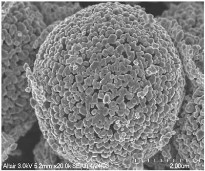
Figure 13-1. TiO2 particles (micron scale formed from nanoscale particles, used for clarity). (Courtesy of Altair Nanotechnologies, Inc.)
Remember white, pasty sunscreen? It is now transparent because the key ingredient, zinc oxide, which absorbs ultraviolet light, is transparent if it is made of nanoparticles but white when made of larger, micron-sized particles. The same holds for titanium dioxide—which is a white paint pigment and an additive to improve opacity in colored paints—if the particles are hundreds of nanometers in diameter or greater. Now, these transparent nanoparticles, which still absorb in the UV range, are finding their way into modern, transparent, and highly effective sunscreens.[3]
Nanoparticles of titania are also a key ingredient in dye-sensitized solar cells. The efficiency of these cells is boosted by incorporating nanoparticles that increase the total surface area for harvesting light by a factor of a thousand as compared with a single crystal of titania.[4] Compared with silicon-based photovoltaic materials, dye-sensitized solar cells are much less expensive to produce, and in 2001 a manufacturing plant opened in Australia.[5]
Another significant market for nanoparticles is in the semiconductor industry, in a process known as chemical mechanical planarization (CMP). In the manufacturing of computer chips, the component materials must be coated onto wafers, and at several points in the process, the coatings must be rendered nearly atomically smooth across the entire wafer. For 300-mm wafers, this is no small challenge! In CMP, slurries of nanoparticles are used. In this process, a combination of chemical removal and mechanical abrasion acts to accomplish this atomic-level polishing task. Silica, alumina, and ceria nanoparticles, the most common materials, are very effective. As a result, the global market for CMP has grown rapidly, from $250 million in 1996 to more than $1 billion in 2000, with the market for CMP consumables alone (slurries and polishing pads) expected to hit $800 million by 2005.[6] With ever-increasing miniaturization in device features, resulting in a need for increasing precision in manufacturing, the CMP market will surely continue to grow.
In addition to these existing large-scale applications for nanoparticles, many more products have been recently commercialized or are in development. Professors Paul Alivisatos of the University of California, Berkeley, and Moungi Bawendi of MIT developed processes for making semiconducting nanoparticles out of materials including cadmium selenide (CdS) and cadmium telluride (CdTe). These particles, coated with zinc sulfide, absorb light in the UV range, and then because of size-dependent quantum confinement effects, they emit light in the visible range, at a wavelength dependent on the particle size. Their stability and brightness are much better than those of conventional fluorescent chemical dyes, and when they are functionalized with proteins, oligonucleotides, or smaller molecules of interest, they can be used for fluorescent labeling applications in biotechnology.[7] Silicon nanocrystals less than 4nm in diameter also emit light in the visible range, with the wavelength depending on particle size. These nanoparticles are of interest for solid-state lighting applications and promise much higher efficiency as well as longer lifetimes compared with current incandescent and fluorescent lighting technology.[8]
As well as these optical properties of nanoparticles, chemical properties—in particular, catalytic activity—can be greatly improved at the nanoscale. One important example is gold. In bulk form, gold is relatively inert. However, when deposited at very low concentrations (0.2 to 0.9 atomic %) in a nonmetallic form onto nanoparticles of cerium dioxide, it becomes very active for the water–gas shift reaction.[9] In this reaction, carbon monoxide and water are converted to carbon dioxide and hydrogen. For fuel cells that are powered by hydrocarbon fuels, converted first to hydrogen and carbon-containing by-products, the water–gas shift reaction is key for maximizing the amount of hydrogen while minimizing the amount of carbon monoxide, a molecule that poisons the electrocatalysts in the fuel cell itself. Because of the small amount of precious metal used in this material, the economics are favorable compared with catalysts that contain precious metals at up to 10% atomic percent concentration.
Magnetic properties of nanoparticles can also be exploited—for example, the tendency of small magnetic nanoparticles to be superparamagnetic. Superparamagnetic nanoparticles, in the absence of a magnetic field, have random magnetic moments at temperatures above their Curie temperature, but in the presence of an external magnetic field, they align with the field, producing a high magnetic moment. One application of this phenomenon is in magnetic resonance imaging (MRI). MRI contrast is aided in the body by the presence of naturally occurring materials such as deoxyhemoglobin but can be greatly enhanced by introduction of superparamagnetic iron oxide nanoparticles (SPIONs). These particles have cores consisting of magnetite (Fe3O4), maghemite (gamma Fe2O3), or some combination of both, and are coated to enhance colloidal stability and biocompatibility. The type of contrast enhancement enhanced by SPION is useful in the imaging of features that contain large amounts of fluid, such as internal injuries or cancerous lesions. These nanoparticles are commercially available from several sources.[10] The surface of the SPION can be further functionalized to engineer interactions between the contrast agents and specific tissue and cell types, and this is an active area of research.[11]
Production methods for nanoparticles can be loosely classified into three general categories: wet synthesis, dry synthesis, and milling. In both wet and dry synthesis, nanoparticles are generally produced in a bottom-up way from atomic precursors, whereas in the milling approach, nanoparticles are produced from the top down by mechanically breaking down larger particles. Wet approaches include sol-gel and precipitation methods, whereas dry approaches encompass combustion, furnace, and plasma synthesis of nanoparticles.
In all cases, there are concerns about the narrowness of the size distribution of the nanoparticles, and concern about the degree of agglomeration. All processes for making nanoparticles lead to some spread in the particle size. The size distribution can be modified somewhat by adjusting the process parameters, or the size distribution can be tailored by removing the tails of the distribution through additional separation steps. This typically leads to lower process yield. With respect to agglomeration, nanoparticles have a high ratio of surface area to volume, and it is much more energetically favorable for them to reduce their surface area by coalescing together. Thus, materials that melt at high temperatures if they are in bulk form may fuse together at much lower temperatures if they are nanoparticles.
Some applications, such as the fluorescing quantum dots mentioned earlier, have very tight requirements for particle size and aggregation. Other applications, such as CMP slurries, may not have such narrow constraints. There is no one perfect process. Milling is very energy-intensive, and it may not work at all for some materials, such as pure metals, that are malleable. Precipitation methods may require the addition of capping ligands to the nanoparticle suspension, to stop particle growth and to prevent the particles from agglomerating together. These ligands bind to the surface of the particles, and if they do not impart the desired functionality to the particles, they must be displaced in a separate processing step.
In high-temperature synthesis of nanoparticles, agglomeration can be avoided for some materials by simultaneously quenching and diluting, but this presents a challenge when the process is scaled up. If the nanoparticles suspended in the gas are more dilute, more energy is required to recover them. For some materials that are viscous glasses at high temperature, such as silica, diluting and quenching may not help. Some processes, such as electro-spray or plasma-based syntheses, produce particles that are highly charged, and this aids in reducing agglomeration.
Before a process can be considered commercially viable, there are additional economic concerns. Many processes for nanoparticles have been developed at the laboratory scale, but they are not yet commercialized because of constraints, including scalability considerations and precursor costs. Aerosol pyrolysis—the process used to make nanoparticles of silica, alumina, and titania by companies such as Cabot, Degussa, and DuPont—has long been in existence. Plasma-based processes, because of their potential for high-throughput reduced agglomeration, have been more recently scaled up in industry.[12] Many other processes could perhaps be scaled up, but there is a catch-22 involved: Without a sufficient commercial market for the nanoparticles, there are insufficient resources available for process development. Without sufficient quantities of nanoparticles available, it is difficult to conduct product development research.
In the past several years, there has been increasing public concern about the occupational and environmental risks associated with nanoparticles.[13] The correlation between particle phase air pollution and adverse health effects has been noted for some time.[14] There is now concern that nanoparticles may also threaten human health and ecosystems. It is important to consider that materials that may not pose health risks in bulk may become toxic in nanoparticle form because of their small size. Safety precautions that are appropriate for materials in bulk form may prove insufficient for nanoparticles. As a result, research into potential health risks associated with these new materials, supported by U.S. government agencies such as the Environmental Protection Agency and the National Science Foundation, is actively under way.
Since their discovery in 1991 by Sumio Iijima, carbon nanotubes have fascinated scientists with their extraordinary properties.[1] Carbon nanotubes are often described as a graphene sheet rolled up into the shape of cylinder. To be precise, they are graphene cylinders about 1–2nm in diameter and capped with end-containing pentagonal rings. One would imagine that a new chemical such as this would be discovered by a chemist, slaving away in front of a series of Bunsen burners and highly reactive chemicals, with a sudden epiphany being revealed in a flurry of smoke or precipitation from a bubbling flask. However, carbon nanotubes were discovered by an electron microscopist while examining deposits on the surface of a cathode; he was performing experiments involving the production of fullerenes, or buckyballs.
This discovery presents one of the key tenets of nanotechnology. Novel tools allow researchers to observe materials and properties at the nanoscale that often have existed for hundreds or thousands of years and to exploit the properties of such materials.
After Iijima’s fantastic discovery, various methods were exploited to produce carbon nanotubes in sufficient quantities to be further studied. Some of the methods included arc discharge, laser ablation, and chemical vapor deposition (CVD).[2] The general principle of nanotube growth involves producing reactive carbon atoms at a very high temperature; these atoms then accumulate in regular patterns on the surface of metal particles that stabilize the formation of the fullerenes, resulting in a long chain of assembled carbon atoms.
The arc-discharge methodology produced large quantities of multiwalled nanotubes (MWNTs), typically greater than 5nm in diameter, which have multiple carbon shells in a structure resembling that of a Russian doll. In recent years, single-walled nanotubes (SWNTs) using this method also have been grown and have become available in large quantities. The laser ablation method of carbon nanotube growth produced SWNTs of excellent quality but requires high-powered lasers while producing small quantities of material. The CVD method was pioneered by Nobel Laureate Richard Smalley and colleagues at Rice University, whose experience with fullerenes is nothing short of legendary. This growth technique is aided by a wealth of well-known inorganic chemicals specifically involving the formation of highly efficient catalysts of transition metals to produce primarily single-walled nanotubes.
Figure 13-2 shows a simple carbon nanotube.

Figure 13-2. A simple example of a carbon nanotube. (Courtesy of Dr. Peter Burke, University of California, Irvine.)
Although carbon nanotubes have a suitably interesting structure, there are a multitude of important properties that impart the potential for novel applications of significant commercial value. Multiwalled and single-walled nanotubes have similar properties, and for illustration, focusing on single-walled nanotubes provides a reasonable primer of the primary features.
Some of these properties include remarkable strength, high elasticity, and large thermal conductivity and current density. Several reports have determined that SWNTs have a strength of between 50 and 100 times that of steel.[3] The elasticity of SWNT is 1–1.2 terrapascal (TPa), a measure of the ability of a material to return to its original form after being deformed. Imagine a molecule that, on the atomic scale, is as strong as steel but flexible like a rubber band!
Despite these structural properties, SWNTs have a thermal conductivity almost as great as twice that of diamond, which is known to be one of the best conductors of heat. Perhaps one of the most impressive properties of SWNTs involves their electrical conductivity, which is reported to be 109 Amps per square centimeter, which is about 100 times that reported in copper, the conductor of choice for nearly every electrical device in common use today.
SWNTs have two types of structural forms, which impart an additional set of electrical characteristics. Depending upon the alignment of the carbon atoms in the cylindrical form, SWNTs can be either achiral (having atomic uniformity along its axis) or chiral (having a twisted alignment from the uniform case). Achiral and chiral forms can act as metals or semiconductors and yet retain the same basic nanotube structural motif.
In addition to these well-known properties, SWNTs have other features that make them attractive beyond their scientific novelty. SWNTs have a density approximately half that of aluminum, making them an extremely light material. SWNTs are stable at temperatures up to 2700°C under vacuum. This is truly impressive considering the melting point of Ruthenium, Iridium, and Niobium metals are about the same temperature.[4] Although nanotubes have structural uniformity, the carbon atoms within them have the same precise features as a typical graphene sheet. These atoms can be derivitized to alter the structure of the SWNTs, allowing their properties to be tailored. This allows nanotubes to be subject to literally hundreds of years of rich organic chemistry.
Carbon nanotubes not only can be functionalized to change their structure but also can interact beneficially with organic chemicals that have biological usefulness. Fullerene materials have been explored for use as antioxidants, drug-delivery agents, and amino acid replacements; the latter could lead to new drug candidates. Reports have been published of their benefits in enhancing virus-specific antibody responses or as a scaffold for growing retinal epithelial cells to be transplanted into the retina to treat macular degeneration.[5]
Carbon nanotube synthesis in recent years has been driven by yields and cost. To move nanotubes from scientific curiosity to practicality, they must be available in sufficient quantities at a reasonable cost with high uniformity and reproducibility. In the case of MWNTs, the arc-discharge method provides a good alternative, yielding large quantities of material at a good cost. In the case of SWNTs, while generating large quantities of material, the purity is often unacceptable for a subset of applications because of excessive carbonaceous contamination. Instead, the CVD method and a recent alternative, plasma-enhanced chemical vapor deposition (PECVD), have burst onto the scene as the methods of choice for producing large quantities of SWNTs with micron lengths, purity, and reliability within specifications for certain applications. Figure 13-3 shows an example of PECVD nanotubes.

PECVD has been reported to lower the temperature of nanotube growth significantly by using a plasma to generate the reactive carbon atoms instead of very high temperatures, as in standard CVD growth. In the case of nanoelectronics—perhaps one of the early applications for which SWNTs will be adopted—extremely high purity nanotubes are required, and only a few providers have managed to generate such materials at a reasonable cost.
The key issue with respect to commercial use of nanotubes for most applications comes in placing wafers on silicon or silicon on insulators, which are typical substrates for making circuits or devices. To the extent that alignment or specific orientation is required, applicability has been limited. Two general methodologies exist for proceeding toward manufacturability of devices: specific growth using prepatterned catalysts (Figure 13-4), or patterning of nonoriented fabrics using application of solutions. In the former case catalysts are placed in specific regions of a substrate onto which nanotubes grow in either a vertical or a horizontal direction.
Vertically oriented growth has been demonstrated by several groups and is especially valuable for field emitting devices. Many potential CNT device approaches using CVD growth of SWNTs suffer from manufacturability and scalability issues, primarily because typical CVD temperatures are >800°C for SWNTs. At such high temperatures, other steps in a fabrication process can be adversely affected, causing the yields of working devices to be lower. Indeed this a serious limitation if the underlying substrate or control electronics cannot withstand such temperatures. Some reports have presented data on lower-temperature methods of growing SWNTs using techniques such as PECVD. These techniques are still in their infancy but could represent a reasonable pathway for certain types of devices or applications.
Horizontal fabrics have been applied to substrates whose thickness can be controlled by solution concentration and application procedure. Such methods have conquered the issues of purification of nanotube solutions, distribution of networks of nanotubes of uniform density over large substrates, and patterning of traces of conductive nanotubes into shapes that can be further integrated into complicated process flows.
SWNTs can be obtained in bulk from various suppliers, which have exploited advanced CVD techniques to grow SWNTs in large scale of excellent quality. These nanotubes can then be purified to remove metallic contaminants (for example, Group IA and IIA elements) used in the growth process and carbonaceous species that serve as a potential source of contamination. The processed SWNTs are solubilized and can then be applied to device substrates for further processing.
A variety of potential applications exist for carbon nanotubes. MWNTs have been reported for use primarily as a composite for batteries and as field emitters for television monitors.[6] As the price for these materials continues to drop, other potential applications, especially as additives in composites, are likely.
The molecular nature of carbon nanotube fabrics allows various CNT physical properties, including electromagnetic, mechanical, chemical, and optical behaviors, to be exploited to create integrated electronic devices (including nonvolatile memory devices); chemical, biological, and radiation sensors; passive low-resistance, low-capacitance conformal interconnects; and electromagnetic field emission devices, scaffolds for cell growth, antioxidants, and near infrared imaging tags for biological samples and cells, to name a few. Table 13-1 summarizes a number of proposed applications that could use SWNT fabrics as an enabling component.[7]
Table 13-1. Sample applications of single-walled carbon nanotube fabrics.
Semiconductors | Life Sciences | Instrumentation |
|---|---|---|
Nonvolatile and volatile memory | Membranes | Mechanical relays and switches |
Programmable logic devices | Chemical absorption | Thermal sensors and actuators |
Global and local interconnects | Valves | Acceleration sensors |
Inductors | Nanomixers | Bolometers |
Radio frequency (RF) components | Heat exchangers | Gyroscopes |
Micromirrors | Nanochannels | Field emission tips displays |
Chip-to-chip interconnects | Reaction chambers | Acoustic/Pressure sensors |
Transistors | Nanofluidics devices | Radiation detectors |
One existing application for which SWNTs are particularly useful is in the arena of electronics, specifically to create nonvolatile memory.[8] In the case of nonvolatile memory applications, significant progress has been made in using fabrics, or assemblages of SWNTs, as electrical traces within integrated circuits.[9] These fabrics retain their molecular-level properties while eliminating the need for nanoscale physical control. These monolayers are created by room-temperature spin-coating of a solution of SWNTs in a semiconductor-grade solvent. After evaporation of the solvent, the resulting monolayer fabric is lithographically patterned and etched in an oxygen plasma. The process of spin-coating SWNT solutions can be used to produce monolayer fabric of very steep aspect ratios, which allows coverage of fabrics over sharp edges or tall structures. Such diversity in the coating of nanotube fabrics on three-dimensional structures has the potential to support traditional horizontal integration schemes in electronics as well as a novel set of devices oriented in a vertical fashion that could lead to significantly more dense electronics.
The combination of patterned nanotube fabrics and the use of fabricated sacrificial layers around the fabric allows the formation of an open cavity, in which a suspended patch of fabric can be mechanically drawn into electrical contact with an electrode. These devices, called molecular microswitches (MMSs), can be used as storage elements for memory or logic applications.
The SWNT fabric approach uses a 1–2-nm thick patterned SWNT fabric and can be interconnected monolithically with additional standard semiconductor (for example, CMOS) circuitry above or below, providing buffering and drive circuitry to address and control the MMS devices. When this technique is used, the limit to the scalability of the hybrid nanotube/ CMOS system depends only on the available photolithographic node. Hence, the CMOS fabrication, and not the inclusion of nanotubes, remains the limiting factor in scaling. Indeed, the ultimate physical limit to the integration density of this approach scales down to two individual metallic nanotubes and their electromechanical interaction.
| 1. | S. Iijima, Nature 354, (1991): 56. |
| 2. | C. Journet et al., Nature 388 (1997): 756; A. Thess et al., Science 273 (1996): 483; and A. M. Cassell, J. A. Raymakers, J. Kong, and H. Dai, J. Phys. Chem. B 103 (1999): 6484. |
| 3. | T. W. Ebbesen et al., Nature 382 (1996): 54; M. M. J. Treacy, T. W. Ebbesen, and J. M. Gibson, Nature 381 (1996): 678; and J. W. Mintmire, B. I. Dunlap, and C. T. White, Phys Rev Lett 68 (1992): 631. |
| 4. | http://www.lenntech.com/Periodic-chart-elements/melting-point.htm. |
| 5. | D. Pantarotto et al., Chem Biol. 10 (2003): 961. |
| 6. | Y. Chen et al., Appl. Phys. Lett. 78 (2001): 2128; and D. Qian et al., Appl. Phys. Lett. 76 (2000): 2868. |
| 7. | R. H. Baughman, A. A. Zakhidov, and W. A. de Heer, Science 297 (2002): 787. |
| 8. | T. Rueckes et al., Science 298 (2000): 94. |
| 9. | D. K. Brock et al., Proc. 2005 IEEE Aero. Conf. (2005). |
Zhong Lin Wang
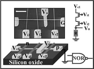
Semiconductor nanowires (NWs) are wires only a few nanometers in size that do not occur naturally. They represent an important broad class of nanometer-scale wire structures, which can be rationally and predictably synthesized in single-crystal form with all their key parameters controlled during growth: chemical composition, diameter, length, doping, and so on. Semiconductor NWs thus represent one of best-defined and best-controlled classes of nanoscale building blocks, which correspondingly have enabled a wide range of devices and integration strategies (Figure 13-5). For example, semiconductor NWs have been assembled into nanometer-scale field effect transistors (FETs), p-n diodes, light-emitting diodes (LEDs), bipolar junction transistors, complementary inverters, complex logic gates, and even computational circuits that have been used to carry out basic digital calculations. It is possible to combine distinct NW building blocks in ways not possible in conventional electronics. Leveraging the knowledge base of chemical modifications of inorganic surfaces can produce semiconductor NW devices that achieve new functions and produce novel device concepts.
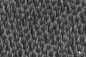
Figure 13-5. Aligned semiconducting ZnO nanowire arrays. These wires are grown uniformly from a solid substrate, and their location and density can be defined by the deposited catalyst of gold.
Semiconducting oxide nanobelts (NBs) are another unique group of quasi-one-dimensional nanomaterials with well-defined side surfaces, which have been systematically studied for a wide range of materials having distinct chemical compositions and crystallographic structures. Beltlike, nanobelts (also called nanoribbons) have been synthesized for semiconducting oxides of zinc (Figure 13-6), tin, indium, cadmium, and gallium by simply evaporating the desired commercial metal oxide powders at high temperatures. These oxide nanobelts are pure, structurally uniform, single-crystalline, and largely free of imperfections; they have a rectangularlike cross section with controllable dimension. Field effect transistors and ultrasensitive nanosize gas sensors, nanoresonators, and nanocantilevers have also been fabricated based on individual nanobelts. Thermal transport along the nanobelt has also been measured. Nanobelts, nanosprings, and nanorings that exhibit piezoelectric properties have been synthesized that could eventually be used to make nanoscale traducers, actuators, and sensors.

Figure 13-6. Nanobelt of ZnO synthesized by a vapor-solid process. The nanobelt has a well-defined side surface, and it usually has a rectangular cross section.
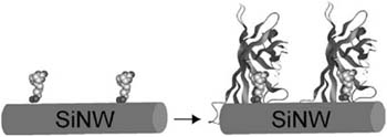
Because many biological molecules, such as proteins and DNA, are charged under physiological conditions, it is also possible to detect the binding of these macromolecules to the surface of nanowires. Protein detection by SiNW nanosensors has been demonstrated for the well-characterized ligand-receptor binding of biotin-streptavidin (Figure 13-7) using biotin-modified NW surfaces.
In direct band gap semiconductors like InP, the p-n junction also forms the basis for critical optoelectronic devices, including LEDs and lasers (see Figure 13-8). To assess whether our crossed NW devices might behave similarly, the photoluminescence (PL) and electroluminescence (EL) from crossed NW p-n junctions can provide a means for controlling the color of the LEDs in a well-defined way. The ability to tune color with size in these nanoLEDs might be especially useful in future nanophotonic applications.

The controlled high-yield assembly of crossed NW p-n diodes and crossed-nanowire field effect transmitters with attractive device characteristics, such as high gain, enable the bottom-up approach to be used for assembly of more complex and functional electronic circuits such as logic gates. Logic gates are critical blocks of the hardware in current computing systems that produce a logic-1 and logic-0 output when the input logic requirements are satisfied.
Diodes and transistors represent two basic device elements in logic gates. Transistors are more typically used in current computing systems because they can exhibit voltage gain. Diodes do not usually exhibit voltage gain, although they may also be desirable in some cases. For example, the architecture and constraints on the assembly of nanoelectronics might be simplified using diodes because they are two-terminal rather than three-terminal transistors. In addition, by combining the diodes and transistors in logic circuits, it is possible to achieve high voltage gain while simultaneously maintaining a simplified device architecture. The flexibility of these NW device elements for both diode- and FET-based logic has been demonstrated in the creation of AND, OR, NOR gates that have been used to implement simple basic computation (Figure 13-9).
For applications in nanotechnology, ZnO has three key advantages. First, it is a semiconductor that has a direct wide-band gap and significant excitation-binding energy. It is an important functional oxide, exhibiting near-UV emission and transparent conductivity at room temperature and higher. It is also piezoelectric because of its noncentral symmetry. This is a key phenomenon in building electromechanical coupled sensors and transducers at nanoscale. The piezoelectric coefficient of a polar nanobelt is about three times that of bulk material, and this makes it a candidate for nanoscale electromechanical coupling devices. Finally, ZnO may be biosafe and biocompatible, so it can be used for biomedical applications without coating. With these three unique characteristics, ZnO could be one of the most important nanomaterials in future research and applications. The diversity of nanostructures presented here for ZnO should open many fields of research in nanotechnology.
The synthesis of various nanostructures is based on a solid-state thermal sublimation process, in which a pile of source materials, typically the powder form of oxides, is placed at the center of a tube furnace. The source materials are sublimated by raising the temperature of the furnace; a redeposit ion of the vapor phase at a lower temperature zone produces novel nanostructures. By controlling the growth kinetics, the local growth temperature, and the chemical composition of the source materials, researchers have synthesized a wide range of polar-surface dominated nanostructures of ZnO under well-controlled conditions at high yield (Figure 13-10).
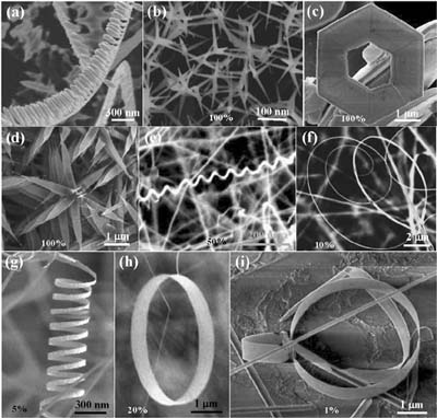
Figure 13-10. A collection of polar-surface induced/dominated nanostructures of ZnO, synthesized under controlled conditions by thermal evaporation of solid powders unless specified otherwise: (a) nanocombs induced by asymmetric growth on the Zn-(0001) surface; (b) tetraleg structure due to catalytically active Zn-(0001) surfaces; (c) hexagonal disks or rings synthesized by solution-based chemical synthesis; (d) nanopropellers created by fast growth; (e) deformation-free nanohelixes as a result of block-by-block self-assembly; (f) spiral of a nanobelt with increased thickness along the length; (g) nanosprings; (h) single-crystal seamless nanoring formed by loop-by-loop coiling of a polar nanobelt; (i) a nanoarchitecture composed of a nanorod, nanobow, and nanoring. The percentage in each figure indicates the purity of the as-synthesized sample for the specific nanostructure in a specific local temperature region.
Zinc oxide (ZnO) is a material that has key applications in catalysts, sensors, lasering, piezoelectric transducers, transparent conductors, and surface acoustic wave devices. This chapter focuses on the formation of various nanostructures of ZnO, showing their structures, growth mechanisms, and potential applications in optoelectronics, sensors, transducers, and biomedical science. For the nonpolar surfaces of ZnO, various forms of nanostructures have been synthesized for ZnO (Figure 13-11). These structures were realized by controlling growth kinetics.

Figure 13-11. A collection of nonpolar-surface dominated nanostructures of ZnO, synthesized under controlled conditions by thermal evaporation of solid powders by controlling source materials, growth temperature, temperature gradient, and substrate. (a) Nanobelt; (b) aligned nanowire arrays; (c) nanotubes; (d) array of propellers; (e) mesoporous nanowires; (f) cages and shell structures; and (g) hierarchical shell and propeller structure. The percentage in each figure indicates the purity of the as-synthesized sample for the specific nanostructure in a specific local temperature region.
Many soft or fluid consumer products—such as foods, paint, detergents, personal care products, and cosmetics—contain nanometer- to micrometer-scale structures. These structures are formed by the spontaneous self-assembly of natural or synthetic surfactants or block copolymers. In many cases, to create the desired structure and performance, complex mixtures of different surfactants and polymers are required.
Figure 13-12 shows an example of a simple, nonionic surfactant. Figure 13-13 illustrates some of the soft nanoscale structures that form spontaneously in surfactant or block copolymer solution. The particular structure that is formed depends on the relative sizes of the head and tail and their chemical character. For example, surfactants that have ionic (charged) head groups often form spherical micelles, whereas non-ionic (uncharged) surfactants are more likely to form rodlike structures, and surfactants that have more than one tail are more likely to form vesicles or lamella (almost flat sheets). The soft nanoscale structure can also be influenced by the order of addition of the different ingredients.

Figure 13-12. A simple example of a surfactant, in this case a non-ionic ethoxylate surfactant, shown as the chemical structure (top), as a space-filling molecular model (bottom left), and as a cartoon representation (bottom right).

Figure 13-13. Cartoon representations of different surfactants forming a spherical micelle (top), a rodlike micelle (middle), and a vesicle (bottom) in water. A slice through each of the nanostructures is shown; in the complete structures, the hydrophilic head groups surround the hydrophobic tails, shielding them from unfavorable interactions with water.
These soft nanostructures do work on demand. When you add dish liquid to hot water in a dishpan full of dirty pots and pans, the nanoscale structure of the surfactant micelles change as they migrate to the oily surfaces, encapsulate the grease, and carry it into solution. When you paint a wall with a good-quality emulsion-based paint, the brush moves easily as you spread the paint on the wall, but as soon as you finish brushing an area, the structure changes and the viscosity of the paint increases to reduce the occurrence of drips. Soft nanotechnology is also at work when you mix up a cake or even enjoy the taste and texture of chocolate, ice cream, or yogurt.
Designing these complex materials is difficult, and characterizing them is challenging. Until recently, most soft nanostructured products were created by experienced formulators, using empirical rules that were passed down through generations of product developers. Although ideas of self-assembly were invoked to explain behavior, it was almost impossible to predict what structure would be created from a particular mixture of ingredients. And because it was extremely difficult to characterize products that were known to be successful, it was hard to know what structure was desirable for a particular application.
Today, new methods of characterization are providing insight into soft nanostructured materials—for example, dynamic light scattering, NMR diffusion experiments, X-ray and neutron scattering, and electron microscopy. New robotics techniques are allowing developers to explore many more formulas than was possible when each candidate formula had to be created by hand. New theories and computer simulation methods are enabling researchers to construct realistic models of soft nanostructured materials. Taken together, these developments have the potential to revolutionize consumer product development.
Other members of the nanotechnology community are also becoming interested in self-assembly and nanostructured fluids, which indeed have the potential to provide robust and inexpensive strategies for creating nanoscale materials. For example, IBM recently highlighted the potential for block-copolymer self-assembly to create nanometer-size structures for electronics applications. Several groups are exploring strategies for creating hard nanoparticles using soft self-assembled structures as templates, and self-assembled block copolymer-stabilized emulsions and vesicles are being proposed as drug- (and nutriceutical-) delivery devices. Moreover, various soft nanotech strategies are being applied to stabilize colloidal systems (nanoparticle solutions and gels).