
MPPT Efficiency: Noise Sources and Methods for Reducing Their Effects
3.1 Low-Frequency Disturbances in Single-Phase Applications
AC applications of PV systems require a power processing element able to convert the DC power generated by the PV unit into AC power, at 110 or 230 V rms voltage rating by adapting the PV voltage to that needed by the stage performing DC/AC conversion. The adoption of single-stage power processing units is the best choice, especially from the point of view of reliability and efficiency. Some commercial solutions, especially in the power range of interest for residential power plants (e.g., from Fronius and SMA), are based on the topology depicted in Figure 3.1, which consists of only a pulse-width modulation (PWM) inverter controlled in such a way that the maximum power from the PV source is extracted and an almost pure sinusoidal current is injected into the grid or into an AC stand-alone system with energy backup.
Because of the inherent step-down characteristic of the inverting bridge, the adoption of a single-stage inverter requires that the PV voltage be higher than the peak AC voltage value, so that this solution is not suitable for low-power PV applications like microinverters.
Double-stage or multiple-stage solutions are based on a DC/DC converter that controls the PV source and performs the MPPT function, cascaded by a DC/AC conversion stage. Such architecture is shown in Figure 3.2, where the bulk capacitance, placed between the two conversion stages, plays an important role.
The bulk capacitance, indeed, handles the imbalance between the PV power made available at the DC bus by the DC/DC stage and the AC power absorbed by the grid through the DC/AC stage. The difference between the DC power and the AC power is a sinusoidal component at twice the AC grid frequency, namely, either 100 or 120 Hz, as shown in Figures 3.2 and 3.3. The amplitude of the voltage oscillation across the bulk capacitor due to the AC power component can be easily calculated by assuming that the bulk capacitor current has the following expression:
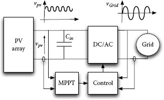
FIGURE 3.1
Single-stage, single-phase PV inverter.
(3.1) |
where ωgrid is the grid frequency. The AC component of the bulk voltage is then given by
ˆvb(t)=IbCb⋅∫Tgridcos(2⋅ωgrid⋅t)dt=Ib2⋅ωgrid⋅Cb⋅sin(2⋅ωgrid⋅t) |
(3.2) |
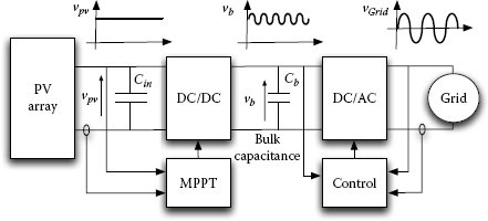
FIGURE 3.2
Double-stage, single-phase PV inverter.
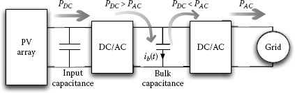
FIGURE 3.3
Role of the bulk capacitance.
and the peak-to-peak value of the voltage oscillation at a frequency 2 · ωgrid is
(3.3) |
where the PV power has been assumed to be PPV = Vb·Ib. Equation (3.3) reveals that the voltage oscillation amplitude is not constant along the day, because it depends on the instantaneous PV power, namely on the irradiation level.
The oscillation affecting the voltage of the bulk capacitor has detrimental effects on both the DC and the AC part of the power processing system, so that a large electrolytic capacitor is mostly used at the DC link. In fact, as (3.3) highlights, the larger the bulk capacitance, the smaller the voltage oscillation. Unfortunately, bulk electrolytic capacitors are a weak point of the conversion chain, because of the effects that the operation temperature has on their lifetime. A significant effort is done by PV inverter manufacturers in order to keep the working temperature of the bulk capacitor as close as possible to that at which the capacitor manufacturer has tested the component for some thousands of hours, so that the mean time between failures (MTBF) is increased.
A reduced value of the bulk capacitance might allow use of film capacitors instead of electrolytic ones, but the resulting increased low-frequency oscillation given by (3.2) would have an impact on the quality of the current at the inverter output, so that suitable control techniques must be adopted in order to reduce such an effect.
The oscillation back propagates through the DC/DC converter up to the PV terminals, thus degrading the quality of the MPPT operation performed by the DC/DC converter itself. A simplified expression of the nonlinear current vs. voltage characteristic allows us to obtain a relationship between the amplitude (3.3) and the MPPT efficiency [1]. Neglecting the series and parallel resistances in the PV array model provides the following PV MPP current and relevant derivatives:
(3.4) |
(3.5) |
(3.6) |
These expressions allow us to approximate the PV current vs. voltage curve across the MPP by means of the second-order Taylor series:
(3.7) |
that is,
(3.8) |
where
(3.9) |
(3.10) |
(3.11) |
The oscillation of the bulk voltage causes an oscillation of the PV voltage across the MPP: If M(D) = Vb/VPV is the voltage conversion ratio of the DC/DC converter, then ΔVPV = ΔVb/M(D). The PV voltage is thus given by
(3.12) |
so that the instantaneous power and average power over one period of the grid voltage can be calculated:
pPV(t)=vPV(t)⋅iPV(t) =γ⋅(VMPP+ˆv(t))+β⋅(VMPP+ˆv(t))2+α⋅(VMPP+ˆv(t))3 P=1Tgrid∫Tgridp(t)dt =γ⋅VMPP+β⋅V2MPP+α⋅V3MPP+3⋅α⋅VMPP+β2⋅ΔV2PV =PMPP+3⋅α⋅VMPP+β2⋅ΔV2PV |
(3.13) |
Equation (3.13) can be used to obtain an expression of the MPPT efficiency as a function of the bulk voltage oscillation amplitude:
(3.14) |
The voltage oscillation amplitude that ensures a desired MPPT efficiency [1] is then given by
(3.15) |
Equation (3.14) reveals that the MPPT efficiency is as high as the oscillation amplitude is small. It must be highlighted that α and β are negative; thus the term 3 ·α·VMPP + β appearing in (3.13), (3.14), and (3.15) is negative.
Equation (3.15) provides the constraint to be fulfilled by the oscillation amplitude on the bulk voltage if a desired minimum MPPT efficiency is required. The value of ΔVb given by (3.15) can be put into (3.3) in order to obtain the value of Cb. Equation (3.15) also puts into evidence that a step-up DC/DC converter, characterized by M(D) > 1, allows use of a smaller bulk capacitance for a given MPPT efficiency: The higher M(D), the higher ηMPPT.
The previous discussion highlights the weak point of the single-stage PV inverter topologies. In particular, they include only one storage element, that is, a large electrolytic capacitor, at the PV source terminals, so that a reduction of that capacitance aimed at using more reliable components would cause an increase of the PV voltage oscillation amplitude, with a consequent reduction of the MPPT efficiency. On the contrary, the presence of M(D) in (3.14) and (3.15) highlights that the additional DC/DC converter is very helpful in reducing the effects of the oscillations coming from the DC link, not only at the frequency of the bulk voltage oscillation but also in a wider range of frequencies.
The strategy of using the DC/DC converter as an active filter was presented in [2] and is described in the next section. Some other approaches have also been presented in literature [3]. In some cases they are referred to applications involving fuel cells (FCs). FCs are electrochemical systems that are able to convert a chemical energy vector, e.g., hydrogen or methanol, into electrical power by means of the action of a catalyst and of the contribution of oxygen at the cathode. Similar to PV systems, FCs are low-voltage devices that, in the power range of a few kilowatts, are able to deliver hundreds of amperes in DC. While any disturbance affecting the PV current has only a detrimental effect in terms of MPPT efficiency, current ripple significantly affects the fuel consumption and life span of FCs [4]. In other words, while in PV systems the ripple can be tolerated at the price of a reduced MPPT efficiency, in FC systems the current ripple must be kept below 10% of the average value in order to preserve the stack functionality. As a further difference between the PV and FC systems in this aspect, the effect of the ripple frequency must be pointed out. In PV systems, any oscillation at whichever frequency is detrimental for the MPPT efficiency. In FC applications, instead, the high-frequency ripple, mainly due to the switching operation of the converter, is easily filtered by a small capacitance put in parallel to the stack terminals. Instead, the low-frequency component at 100/120 Hz cannot be passively filtered in an effective way and has a strong impact on the stack aging because of the stresses it causes on the FC membrane.
In [5] a DC/DC converter controlled by means of a double-feedback loop allows us to compensate the 100/120 Hz harmonic component. The latter is caused by a full bridge inverter, connected in cascade with the DC/DC one, thus forming a classical double-stage power processing system that allows injection of the power produced by a fuel cell into the grid. The approach proposed in [5] requires a careful design of the controller, because the interaction between the dynamics of the two loops deeply affects the attenuation capabilities. Low-frequency disturbances can be injected by the outer control loop if its bandwidth is close to the grid frequency.
In [6] a power zero ripple filter (ZRF) has been proposed. The authors point out that the high FC current flowing in the ZRF dramatically increases the conduction losses, so that they suggest a practical implementation involving four ZRFs, with a significant increase of topology and control strategy complexity. In [7] a novel topology called pulse-link DC/AC converter is proposed. An inductor and a capacitor connected in series are inserted between the DC/DC and the DC/AC stages, which increase the complexity and the number of components used in the power processing system. A similar approach is proposed in [8], where the active filter is inserted in the DC/DC converter by using a center tap isolation transformer. Another interesting approach, based on a feed-forward control structure, is proposed in [9]. This technique requires a perfect phase lock of the sinusoidal oscillation at twice the grid frequency, so that the use of an additional phase-locked loop (PLL) circuit is mandatory. Furthermore, as in any feed-forward approach, the proposed technique suffers uncertainties related to unmodeled phenomena and disturbances. Another limitation of the approach proposed in [9] is represented by the fact that the attenuation is obtained only at twice the grid frequency. In practice, the disturbance produced by the AC connection at 100 or 120 Hz is prevailing, but also additional harmonics are generated by the system nonlinearity.
A feed-forward technique is also used in [10]. The method is explained in more detail in [11], where a digital implementation is also proposed. Supposing that the DC/DC converter always operates in a given mode, e.g., continuous conduction mode, the availability of the formula expressing the voltage conversion ratio allows calculation of the correction to be instantaneously given to the duty cycle value in order to compensate the oscillation of the DC/DC converter output voltage and to keep the input voltage constant. Such a correction is at twice the grid frequency, and is superimposed to the stationary duty cycle values driven by the MPPT control loop. The main limitation of this simple and intuitive technique is in the fact that the voltage conversion ratio has to be known in explicit form, which does not change during the system operation. Unfortunately, at low irradiation levels, e.g., at sunrise and sunset, any DC/DC converter based on a classical boost, buck, or buck-boost topology and using diode rectifiers may get close, and even enter, discontinuous conduction mode. In this case the method gives a wrong compensation of the disturbance, unless the discontinuous current operating mode is detected and the right formula is used to predict the correct compensating duty cycle amplitude.
An effective technique for reducing the effects of the noise on the MPPT efficiency consists in employing closed-loop switching converters instead of open-loop ones. Such an approach is described in the next section by referring to the P&O technique.
3.1.1 The Perturb and Observe Approach Applied to Closed-Loop Switching Converters
In Section 2.4.2 the guidelines for settling the parameters Tp and Δx were given. Therein, the assumption that Δx is the only stimulus applied to the system has been adopted in order to explain the basic concept. Unfortunately, it is not fully realistic, except for a PV battery charger where the battery is approximated with a constant voltage generator.
In this section the advantages of using the P&O algorithm on a feedback-compensated switching converter, and based on the scheme of Figure 2.6, will be shown. This approach is particularly suitable for controlling PV systems in the presence of noise at the converter output, which is detrimental for the P&O performances. The benefits of the feedback compensation in the P&O operation will be analyzed, and an example of how to apply the P&O design equation to the closed-loop converters will be proposed.
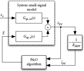
FIGURE 3.4
Effect of output voltage noise on the PV voltage.
The effect of the noise on the PV voltage is described by using the output-to-input Gvp,vo(s) transfer function, as shown in Figure 3.4. In this scheme the converter transfer functions depend on the architecture selected for performing the MPPT.
Both the P&O perturbation (x̂) and the output voltage noise (v̂o) affect the PV voltage. An estimation of the maximum ΔVPV variation is
(3.16) |
where the first term has already been introduced in (2.33) and represents the P&O effect, Gvp,vo(ω) is the magnitude of the output-to-input transfer function evaluated at the noise frequency ω, and ΔVo is the amplitude of the output voltage noise (Vo). Equation (3.16) involves the absolute values because the signs of both voltage variations are not correlated and cannot be predicted in advance. The use of the absolute quantities ensures that we take into account the worst case for the ΔVPV variation. As a consequence, by substituting eq. (3.16) in (2.32) we get
(3.17) |
where the symbols have the same meaning described in Section 2.4.2.
As explained in Section 2.4.2, in order to avoid that the P&O is confused by the effect of additional noise v̂o, the PV power variation produced by a perturbation Δx must be greater than the sum of all the other PV power variations. In this case the P&O step amplitude must fulfill the following inequality:
(3.18) |
In a more compact form,
(3.19) |
where Δx˙G is the step amplitude needed for compensating the irradiance variation and ΔxΔV0 is the step amplitude needed for compensating the output noise. According to the assumption done on (3.16), Equation (3.19) considers the worst case in the evaluation of Δx. It is worth noting that even under a constant irradiance level (Δx˙G=0), the amplitude of the duty cycle perturbation must be large enough in order to overcome the negative effects of the oscillations at the converter output.
Under steady-state atmospheric conditions, it is mandatory to keep Δx as low as possible in order to bound the amplitude of the oscillations of the PV array operating point around the MPP to guarantee a high MPPT efficiency.
A technique for reducing ΔxΔV0 is based on the adoption of a compensation network, with a suitable frequency bandwidth B, able to remove from the PV array voltage all the oscillations due to noises appearing at a frequency lower than B.
The PV voltage vPV is sensed and compared with the output signal of the MPPT controller. As shown in Figure 2.6b, the latter is used to perturb the voltage reference of a closed-loop DC/DC converter. In Figure 3.5 the corresponding small-signal model is shown: It includes the small-signal model of the power stage (Figure 3.4) and of the PV voltage compensation loops.
The objective is to design the transfer function Gc(s) leading to a stable closed-loop system, with an adequate phase margin, with the additional constraint that the closed-loop transfer function Wvp,vo(s) between the converter output voltage and the PV array voltage is sufficiently small at the frequency of the noise to be suppressed. From Figure 3.5, the expression of Wvp,vo(s) is obtained:
(3.20) |
where Tc(s) = Gvp,d (s)·GPWM·Hv·Gc(s) is the loop gain of the system under study. Hv is the gain of the PV voltage sensor and Gpwm is the gain of the PWM modulator, as shown in Figure 3.5.
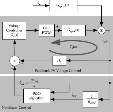
FIGURE 3.5
Small-signal model with a PV voltage compensation network.
The closed-loop transfer function Wvp,vref(s), between ˆvPV(s) and ˆvref(s), is
(3.21) |
with the approximation in (3.21) holding only in the frequencies range where Tc(s) >> 1. Such a condition must be fulfilled within bandwidth B to comply with the wish of suppressing noise whose frequency spectrum falls within B.
Regarding the MPPT algorithm, the closed-loop transfer functions (3.20) and (3.21) have, respectively, the same roles of Gvp,vo(s) and Gvp,x(s) for the open-loop system shown in Figure 3.4. This analogy allows us to fix the right values of the P&O parameters straightforwardly by using the results of the previous discussion. The perturbation period Tp is chosen by analyzing the behavior of ˆp(t)=−ˆv2PV/RMPP and by using (3.21) in order to calculate the response ˆvPV(t) to a small step perturbation ˆvref(t). The amplitude Δvref is instead given by
(3.22) |
namely:
(3.23) |
The effect of ΔVo can be minimized by reducing the value of |Wvp,vo(ω)| as much as possible. Further details concerning the benefits of the voltage-compensated converter for PV applications are given in [2].
3.1.2 Example of P&O Design for a Closed-Loop Boost Converter
Figures 3.6 and 2.12 show the same circuit, but the former one includes a 100 Hz voltage oscillation at the converter output and also the Gc(s) compensation network.
The small-signal model shown in Figure 2.13 allows us to determine the following transfer function Gvp,vo(s):
(3.24) |
with μ = 1 − D and all the other coefficients given in (2.39) and (2.40).
The linear compensation network is designed on the basis of the desired dynamic performances: Given the desired crossover frequency and the phase margin of the system loop gain, the values of the parameters in Gc(s) can be easily determined [12]. In order to get a crossover frequency lower than fsw/10 and a phase margin ϕm > 35°, a PID compensator is used:
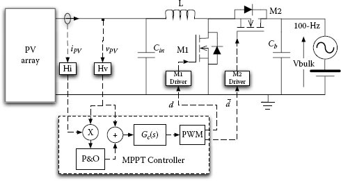
FIGURE 3.6
PV battery charger with a boost converter.
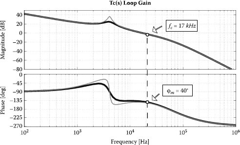
FIGURE 3.7
Bode plots of the converter loop gain Tc(s). Grey curve Tc(s) at G = 100 W/m2, black curve Tc(s) at G = 1000 W/m2.
(3.25) |
The data listed in Table 2.1 lead to the following values of the parameters in Gc(s): k = −6 · 106, ωz1 = 2·104 rad / s, ωz2 = 2.5 · 104 rad / s, ωp1 = 3.105 rad / s, and ωp2 = 4.5 · 105rad / s. With this value the open-loop transfer function guarantees a crossover frequency of fc ≃17 kHz and a phase margin of ϕm ≃ 40°
The transfer function Gvp,d(s) depends on the irradiance level G through the value of the parameter RMPP appearing in the denominator of (2.38). In particular, the value of ζ and the dynamic characteristics (fc, ϕm) of Tc(s) must be designed in the worst case. Figure 3.7 shows the converter loop gain Tc (s) = Gc (s)·GPWM·Gvp,d (s) at a low irradiance level, G = 100 W/m2, and at a high one, G = 1000 W/m2. It is assumed that Hv = 1.
The Bode diagrams show that the compensated system preserves almost the same dynamic performance in any operating condition.
The optimal values of the MPPT controller parameters Tp and Δx = Δvref are designed as follows. Tp is fixed by taking into account the relation (2.22) and by evaluating the step response of the compensated closed-loop transfer function Wvp,vref(s), which is shown in Figure 3.8 together with the corresponding open-loop transfer function Gvp,d(s). Both functions have been evaluated in the worst case in terms of irradiance (G = 100 W/m2). The feedback loop introduces a significant benefit on the speed and damping of the closed-loop system, so that Tp = 0.5 ms can be adopted. This value is five times smaller than that used for Tp if the same boost converter operates in open loop.
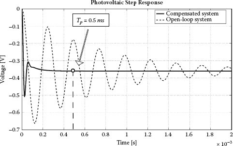
FIGURE 3.8
Step responses of the PV system for low irradiance G = 100 W/m2. Black curve: closed-loop Wvp,x(s) step response; dashed curve: open-loop Gvp,x(s) step response.
The step perturbation Δvref is obtained by means of (3.23). Δvref,˙G is due to the irradiance variation and is evaluated by using the same PV parameters considered in the previous example, namely, RMPP |G=100 ≃ 11Ω, H|G = 100 = 0.0836 A / V2, and Kph = 8mA·m2 / W. The step amplitude required to compensate an irradiance variation ˙G=100 W/m2/s is Δvref,˙G=0.0646V.
Regarding the term Δvref,ΔV0 on the right side of (3.22), a value ΔVo = 3 V has been assumed for the noise at 100 Hz, while the DC component of the bulk voltage has been fixed at 12 V.
The value of |Wvp,vo(ω)| at the noise frequency can be deduced from the Bode diagram shown in Figure 3.9. At f = 100 Hz the system introduces an attenuation of 50 dB, corresponding to |Wvp,vo| = 0.0032, so that the second contribution to the step amplitude needed for compensating the noise is Δvref, ΔVo =|Wvp,vo|·ΔVo = 0.0095V.
Finally, from (3.22), a value of Δvref > 0.0741V must be chosen; in the simulation Δvref = 100 mV is used.
The comparison between Δvref,˙G, and Δvref, ΔVo reveals that in the feedback-compensated system the second contribution is almost negligible.
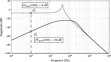
FIGURE 3.9
Bode diagrams (magnitude) of output-to input transfer functions. Dashed line: Gvp,vo(s); continuous line: Wvp,vo(s). Both diagrams have been evaluated at a low irradiance level, G = 100W/m2.
The Bode diagram of Gvp,vo(s) reported in Figure 3.9 highlights the modification of Δ d due to the 100 Hz noise in the scheme analyzed in Section 2.4.3. At 100 Hz the attenuation is 8 dB, corresponding to |Gvp,vo| = 0.4.
Settling the minimum value for Tp = 2.5 ms and applying (2.36) provide the new Δd. The value Δd˙G=0.012 comes from the analysis carried out in Section 2.4.3, while the noise term is ΔdΔV0 = 0.1. The latter value reveals that the configuration proposed in Section 2.4.3 cannot be used in the presence of the 100 Hz noise because it would require a step perturbation that is too high and not feasible by a practical point of view.
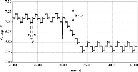
FIGURE 3.10
Steady-state operating conditions of the PV system. Black curve: PV voltage; grey curve: reference voltage Vref imposed by the P&O algorithm with the relative parameters Tp and ΔVref.
The circuit in Figure 3.6 has been simulated at different irradiance levels: G = 1000 W/m2 for t < 25 ms, and G = 100 W/m2 for t > 30 ms. Figure 3.10 shows the behavior of the PV voltage as a function of the voltage reference given by the P&O controller. As explained in Section 2.4.3, the MPPT algorithm, in both stationary irradiance conditions, imposes a three-level oscillation that is confined around the MPP. The transient after the irradiance variation is due to the fact that the MPPT algorithm adjusts the operating point by driving it on a different PV characteristic.
In order to appreciate the benefit of the compensation network, the behavior of the proposed closed-loop system has been compared with the open-loop system designed in Section 2.4.3. In both systems a 100 Hz voltage oscillation of amplitude ΔVo = 3 V has been superimposed on the converter output voltage. Figure 3.11 shows the effect of such an oscillation on the PV voltage. While the closed-loop system does not exhibit a significant PV voltage variation due to the 100 Hz oscillation, the open-loop system is affected by two drawbacks. The first is the poor rejection capability of the converter, which transfers almost totally the output oscillation to the PV terminals. The second is the wrong behavior of the P&O algorithm: The duty cycle is updated with a sequence that does not look like a three-step stairs, as shown in Figure 3.11b. Finally, Figure 3.12 shows that the power generated by the PV source in the close-loop system is very close to the maximum.
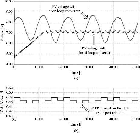
FIGURE 3.11
Steady-state operating conditions with an irradiance level of G = 1000 W/m2. (a) PV voltage in the closed-loop and open-loop systems. (b) Output of the P&O algorithm acting on the duty cycle of the open-loop system.
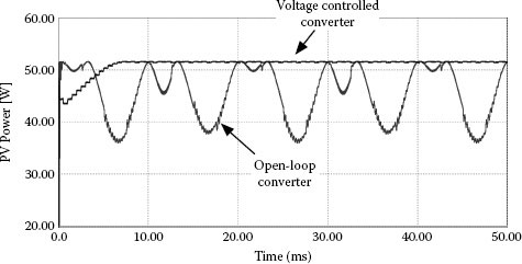
FIGURE 3.12
Instantaneous PV power for a fixed irradiance value of G = 1000 W/m2.
Moreover, the noise rejection capability of the closed-loop system is effective not limited to 100 Hz only, as it extends to the whole range of frequencies below the crossover frequency. As shown in Figure 3.9, Wvp,vo(s) is always much lower than 0 dB. The open-loop system, instead, shows a Gvp,vo(s) that, in some cases, might be even higher than 0 dB, thus producing an amplification of the noise coming from the converter output, with a detrimental effect on the PV power production and on the MPPT operating conditions.
3.2 Instability of the Current-Based MPPT Algorithms
The largest part of the MPPT algorithms presented in literature and used in commercial products is based on the voltage-mode feedback control, or at least on a combination of control loops in which the final objective is to regulate the PV voltage. Indeed, the logarithmic dependency of the PV voltage on the irradiation level makes the MPPT algorithm based on the regulation of the PV voltage less sensible to the irradiance variation [13]. On the other side, the linear dependency of the PV current on the irradiance level would be very useful for a fast current-based MPPT, but the occurrence of irradiance drops might lead to the failure of configurations based on the direct regulation of the PV current. Figure 3.13 shows the basic scheme of a PV current regulator: In terms of MPPT control, it is the dual configuration of Figure 2.6b.
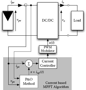
FIGURE 3.13
Control scheme of the current-based MPPT.
The difference in robustness between the voltage-mode-based and current-mode-based MPPT with respect to an irradiance drop is explained in Figures 3.14 and 3.15.
The former shows the I-V and P-V curves at three different irradiance levels. The voltage-based MPPT controller settles the best operating condition (the point marked with the star in Figure 3.14) at a given irradiance level by means of the condition vref = VMPP G(2). In the presence of an irradiance variation (ΔG = ±100 W/m2), at a constant value of the reference voltage, the new steady-state PV operating point is given by the intersection of the vertical line of equation vref = VMPP G(2) with the new I-V and P-V curves. Figure 3.14 shows that regardless of the sign of the irradiance variation, the new operating point is not so far from the new MPP. This means that during the transient, if the MPPT algorithm is not able to change vref promptly, the MPPT efficiency changes, but the system remains under control.
Figure 3.15 shows the same I-V and P-V curves, but with inverted axes: The PV voltage and the PV power are plotted vs. the PV current at three different irradiance levels. The optimal operating condition, marked with the star in Figure 3.14, is fixed at the same irradiance level of the previous case by the current-controlled MPPT technique by imposing iref = IMPP G(2). Where IMPP(G2) corresponds to the current delivered by the PV field when it operates in MPP at the irradiance level G2. At this value of the reference current, in the presence of an irradiance variation, the PV operating point moves vertically. Figure 3.15 shows that an increase of irradiance moves the operating condition far from the new MPP, without compromising the system stability. In fact, the PV field works in the region where the voltage increases slightly and the current is fixed at iref. The wrong behavior occurs in the presence of an irradiance drop: In this case the current-based control can cause a system instability because the PV curves, characterized by the irradiance G3, are on the left side of the vertical line corresponding to the control law iref = IMPP G(2); thus the only possible operating point is at zero voltage. The only way to avoid this voltage drop is to employ an extremely prompt MPPT controller that must be able to change the iref value very quickly.
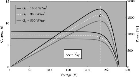
FIGURE 3.14
P-V and I-V curves at different irradiance levels: voltage-based MPPT.
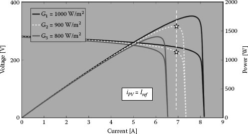
FIGURE 3.15
P-I and V-I curves at different irradiance levels: current-based MPPT.
The maximum irradiance variation that does not trigger this phenomenon in current-based MPPT is estimated as follows. If the optimal operating condition is iref = IMPP G(1) at the irradiance level G1, the minimum allowable irradiance G2 < G1 is given by the condition iref = IMPP G(1) = Isc(G2), where Isc(G2) is the PV short-circuit current at G2.
The relationship between the short-circuit current (ISC) and the irradiance level of a PV cell is given by Isc(G) = Kph·G, and the ratio between the PV current in the MPP and the short-circuit current is almost constant for the different irradiance value. In [13, 2] it is shown that
(3.26) |
where the value of α usually belongs to the interval [0.85 ÷ 0.95]. Imposing
(3.27) |
(3.28) |
and rewriting (3.28) in terms of relative irradiance variation lead to
(3.29) |
By considering the typical value of α, the equation (3.29) reveals that a 5% ÷ 15% drop of the irradiance level can compromise the system stability of an MPPT algorithm performing a direct regulation of the reference current iref. This is the reason why very few examples of current-based MPPT approaches can be found in literature.
Some attempts have been done in order to improve the performance of the current-based approach by suitably modifying the basic structure of the control loop, so that the iref signal is promptly changed in the presence of a rapid irradiance variation. In [15] an inner current loop is coupled with an MPPT-oriented voltage loop to the aim of controlling a grid-connected inverter. In [16, 17] a hysteretic capacitor voltage control is used for the MPPT function in an energy harvesting system, with the main aim of reducing the power consumption of the control circuitry. A robust MPPT current-based architecture adopting the sliding mode control is described in much deeper detail in Section 3.3.
In the previous paragraphs it has been shown that in grid-connected PV systems, like the one depicted in Figure 3.16, the inverter operation generates an oscillation of the voltage of the bulk capacitor Cb at a frequency equal to twice the grid frequency, which propagates through the MPPT DC/DC converter and affects the photovoltaic voltage, thus degrading the MPPT efficiency.
In literature, solutions avoiding large DC-link capacitance Cb have been proposed. They are mostly based on complex architectures that penalize the efficiency and reliability [18]. The linear voltage-mode-based controllers used in [2] and in Section 3.1.1 specifically to reject the disturbances coming from the grid in some cases suffer a possibly not easy design of the compensation network to comply with worst-case conditions and limited robustness whenever both continuous conduction mode (CCM) and discontinuous conduction mode (DCM) operating conditions occur, e.g., during irradiance transitions from high to low levels.
This paragraph shows how the low-frequency ripple mitigation can be achieved by means of the sliding mode control (SMC). Such a nonlinear control technique can be very effective in ensuring extreme robustness and fast response, not only in applications involving switching converters [19,20,21], but also in more complex power electronic systems [22, 23]. SMC is based on the implementation of a control equation, which forces the system variables to stay on a selected surface, called sliding surface.
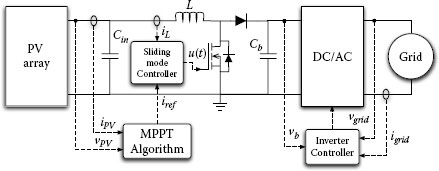
FIGURE 3.16
MPPT P&O with direct perturbation of the reference current.
Many publications available in the literature discuss the SMC. Those ones focused on photovoltaic applications are few and mainly devoted to the control of the DC/AC stage for regulating the current injected into the grid [24, 25].
In this section, the SMC will be used with the specific objective to regulate the PV source in order to remove the 100 Hz disturbance coming from the converter output.
Without loss of generality, the proposed analysis will be carried out by considering the scheme of Figure 3.16. It has been assumed that the first stage of a grid-connected photovoltaic system is a step-up converter used in order to increase the PV voltage to a suitable value that allows the operability of the DC/AC stage. The choice of boost-derived topologies is very common because they provide the additional benefit to sink a continuous current at its input, thus allowing us to minimize the input capacitance.
For the proposed topology, the regulation of the PV field can be easily performed if the SMC is used to control the average input current of the boost converter by imposing the following sliding equation:
(3.30) |
where the reference current iref can be provided by a classical perturbative MPPT controller. Figure 3.17 shows a possible implementation of the SMC with two comparators and a flip-flop. Such a simple scheme can be directly used to generate the signals driving the MOSFET gates:
(3.31) |
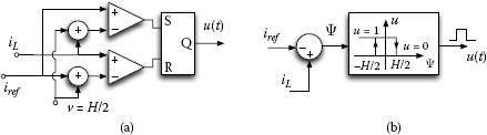
FIGURE 3.17
Sliding mode controller. (a) Practical implementation. (b) Logic scheme.
In steady-state conditions, H(t) fixes the peak-to-peak amplitude of the inductor current ripple and represents the SMC hysteresis band, while iref fixes its average value so that such a control will be identified as sliding mode current control (SMCC).
The analysis of the boost converter leads to the following differential equations:
(3.32) |
where u = 1 means MOSFET turned ON and u = 0 means MOSFET turned OFF.
The necessary and sufficient conditions for local surface reachability are [19,20,21]
(3.33) |
From Equation (3.30), in steady-state condition (iref = constant) the time derivative of the sliding equation is
(3.34) |
Merging Equation (3.33) with (3.34) and using the first row of (3.32) provides
(3.35) |
As in the boost converter, it is vb > vPV > 0; both the previous inequalities are fulfilled. The local stability can be verified by using the following conditions [19]:
(3.36) |
where ueq represents an equivalent continuous control input that maintains the system evolution on the sliding surface.
Substituting the control input u with ueq in Equations (3.30) and (3.32) allows us to write the condition (3.36) in the following way:
(3.37) |
that is,
(3.38) |
where − (vb − vPV)/L corresponds to the inductor current slope when the MOSFET is OFF and vPV/L corresponds to the inductor current slope when the MOSFET is ON. Therefore if the current reference slope is constrained to the inductor current slope, then correct operation of the SMCC is ensured.
In order to analyze the intrinsic capability of the SMCC to reject the noises coming from the output of the converter, the low-frequency equations of the switching converters will be used. These equations are the same used for analyzing the switching converters operating with the PWM modulation; such an approach is still valid because for each signal its average value has been evaluated on a switching period, so that the effect of the low-frequency variation can be analyzed. It is also worth noting that even if the analysis is carried out by focusing the attention on the 100 Hz oscillation of the output voltage, the results can be extended to any disturbances occurring at frequencies lower than 1/10 of the switching frequency, which is the range of validity of the average model [12].
In the following, we will label with fsw(t) the switching frequency (which is time varying in SMCC), with vb0 the average output voltage of the boost converter, and with Δvb(t) the instantaneous deviation of the average output voltage of the boost from vb0 due to the energy storage/release process performed by the bulk capacitor.
The relation among the above quantities is
(3.39) |
In the sequel, we will label with D0 the following quantity:
(3.40) |
The SMC action imposed by Equation (3.31) introduces a natural correction on the duty cycle D(t), which depends on the instantaneous conversion ratio of the converter only. Thus in order to avoid the propagation of the Δvb(t) oscillation on vPV, the duty cycle changes according to the following equation:
(3.41) |
In a PWM control system without any feedback loop, the duty cycle is fixed, and consequently in Equation (3.41), the PV voltage cannot remain constant in the presence of a variation on vb.
The duty cycle fraction ΔD(t) needed to compensate the bulk capacitor voltage oscillation is obtained as follows:
(3.42) |
(3.43) |
(3.44) |
If the waveform Δvb(t) is equal to
(3.45) |
where the amplitude Δvb is given by Equation (3.3), then from (3.44) and (3.45) it is possible to get
(3.46) |
If the inductor current ripple is constant and equal to H0, the switching frequency is given by
(3.47) |
In the sequel we will label with fsw0 the nominal value of fsw:
(3.48) |
The switching frequency oscillation Δfsw(t) can be found by considering that
(3.49) |
(3.50) |
The previous equation shows that the relative oscillation ΔD(t)/D0 of the duty cycle corresponds to the relative oscillation Δfsw(t)/fsw0 of the switching frequency. From Equation (3.46), it is also evident that the duty cycle oscillation does not depend on converter parameters, while the switching frequency oscillations due to the bulk oscillation are related to the inductance and the hysteresis band, as shown in Equation (3.50).
Figure 3.18 shows the waveforms of D(t) and fsw(t) evaluated by means of Equation (3.46) and by using the values reported in Table 3.1.
The main drawback of SMCC is represented by the variability of the switching frequency, which is due to the variation introduced by the DC-link voltage oscillations, which can be estimated with (3.50) and limited with an appropriate selection of the converter parameters, as to the occurrence of DCM operation. In fact, when the current reference is lower than H/2 the lower boundary saturates to zero, increasing in this way the switching frequency to nonsustainable limits. To solve this problem, it is possible to adopt the burst mode (BM) operation [26, 27] when iref < H/2. In this way, it is possible to get the desired average input current by decreasing the switching frequency rather than increasing it.
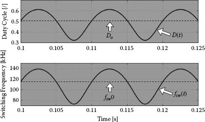
FIGURE 3.18
Low-frequency variation of duty cycle and switching frequency required to compensate the voltage oscillation of vb.
List of Parameters Used in the Simulation
Parameter |
Value |
vPV |
225 V |
vb0 |
460 V |
fgrid |
50 Hz |
fsw0 |
120 kHz |
H0(HysteresisBand) |
2 A |
Ppv ≃ PMPP |
≃1800 W |
Δvb (DC-link voltage oscillation) |
≃127 V |
L |
500 μH |
Cin |
50 μF |
Cb |
30 μF |
Of course, the drawbacks associated to DCM can be overcome by using a synchronous version of the boost converter. In such a case, the boost converter never enters DCM. Another advantage of the synchronous version is represented by its higher efficiency; on the other hand, it is characterized by a higher cost, and also by the need of more complex high-side gate drivers [12].
3.3.1 Noise Rejection by Sliding Mode: Numerical Example
The SMCC has been tested by implementing in the PSIM® circuit-based simulator the scheme of Figure 3.16 [28]. The results have been obtained by considering an irradiance value of G = 1000 W/m2 and ambient temperature of 25°C. The parameters of the DC/DC converter are shown in Table 3.1.
Figure 3.19 reveals the capability of the SMCC to reject the oscillations of vb; although the SMCC is implemented by means of a very simple circuit (Figure 3.17a), the large oscillation appearing on the bulk voltage is almost totally removed from the PV voltage, which is characterized by a DC value only.
Figure 3.20 put in evidence that the duty cycle oscillation (Figure 3.20a) and the switching frequency oscillation (Figure 3.20b) match the analytically predicted behavior of Figure 3.18, thus confirming that the bulk voltage oscillation is translated in a switching frequency oscillation and in an equivalent duty cycle variation, which ensure an almost constant PV voltage.
Unfortunately the pure SMCC suffers stability problems in the presence of fast and large variation in the irradiance conditions. Figures 3.21 and 3.22 show the simulation of the system in Figure 3.16, in which the P&O MPPT algorithm has been used to perturb the reference current iref. The P&O parameters have been settled to the following values: Tp = 15 ms and Δiref = 0.1 A.
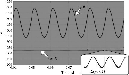
FIGURE 3.19
Waveforms of a PV voltage and bulk voltage.
Two different amplitudes of the irradiance drop have been considered: ΔG = 50 W/m2 and ΔG = 100 W/m2. In the first case, shown in Figure 3.21, at t = 0.3 s the irradiance changes from 1000 to 950 W/m2, and the system experiences a transient after which it is able to reach a new steady-state condition. In the second case, at t = 0.3 s, the irradiance changes from 1000 W/m2 to 900 W/m2, and the system crashes because, after the step irradiance variation, the reference current provided by the MPPT controller is higher than the short-circuit current associated to the new irradiance condition, as shown in Figure 3.22. In this case the higher-threshold iref + H/2 is never reached, creating a sort of stall in the SMCC control. This means that the “hitting condition,” which represents one of the basic constraints in order to achieve SMC, has not been fulfilled [20].
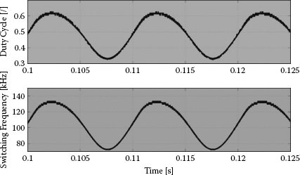
FIGURE 3.20
Duty cycle and switching frequency waveforms in the PSM simulation.
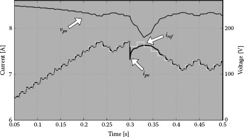
FIGURE 3.21
PV voltage and PV current in the presence of a small irradiance drop.
The wrong behavior in the presence of negative step variations of the irradiance not only affects the SMCC but also occurs in other direct current control strategies without the voltage loop, and it is due to the linear dependency of the PV current with respect to the irradiance. Thus no stability condition is ensured when the PV field works in the region where its behavior is similar to that of a current generator, as explained in Section 3.2.
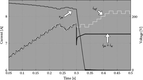
FIGURE 3.22
PV voltage and PV current in the presence of a large irradiance drop.
3.3.2 MPPT Current Control by Sliding Mode
A sliding mode current-based P&O MPPT strategy is described in this section, able to track very promptly the variations in the irradiance value and, additionally, to guarantee the rejection of the low-frequency voltage oscillations affecting the PV array due to the inverter operation in grid-connected systems. The main peculiar aspect of the approach discussed in this section lies in the fact that it is a current-based technique, joining the benefits of a sliding mode inner current loop with the well-known advantages of an outer voltage-based control loop. The inner loop is based on the sensing of the current flowing into the capacitor, which is usually put in parallel with the PV generator. Although the main role of the input capacitor Cin consists in bypassing the switching ripple of the inductor current, in the SMC application herein discussed the PV current control can be obtained by regulating the instantaneous value of the capacitor current. Further details concerning this architecture have been shown in [29,30,31].
3.3.2.1 Basic Configuration of Sliding Mode with Voltage Controller
Figure 3.23 shows a possible control strategy operating on the inductor current of the DC/DC converter in order to regulate the PV current value. The current reference iLref of the inductor current controller is given by
(3.51) |
where iPV is the actual PV current and ivr is the output of the voltage controller. The feed-forward action on iPV considered in (3.51) helps in promptly detecting the irradiation variations and avoid the crashing problems described in the previous paragraph. In steady-state conditions, it is iPV = iLref and ivr = 0.
According to the classical sliding mode DC/DC converter current control theory, the signal u(t) driving the MOSFET is a function of the sliding equation Ψ = iLref(t) − iL(t) = 0, so that the inductor current iL is regulated according to the current reference signal iLref.
At the circuit node connecting the PV array, the boost converter input inductor L and capacitor Cin (see Figure 3.23), it is
(3.52) |
From (3.52) and (3.51), the current reference iLref can be expressed as
(3.53) |
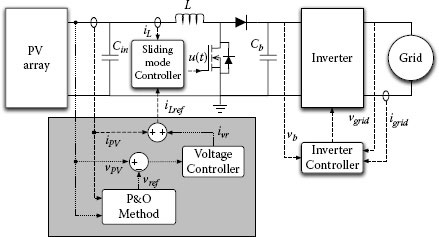
FIGURE 3.23
Sliding mode architecture for compensating the fast PV current variation.
Using the previous expression in the sliding control equation, Ψ = iLref(t) − iL(t) = 0, leads to the following simplification:
(3.54) |
(3.55) |
The simplified control objective (3.55) reveals that the control structure of Figure 3.23 can be simplified as in Figure 3.24, with the inner control loop, which is now aimed at regulating the input capacitance current iCin. This simplification is important because the practical implementation of the scheme shown in Figure 3.23 would require current sensors with too wide bandwidth for iPV and iL, both affecting the value of the MOSFET control signal u(t). Instead, in the scheme of Figure 3.24, u(t) only depends on the instantaneous value of iCin. Consequently, only one wide-bandwidth current sensor is required because the other one, dedicated to iPV, can be narrow bandwidth. Additionally, sensing the capacitor current is easier than for the inductor current due to the fact that the former has a zero DC component. Another advantage of the system shown in Figure 3.24 consists in its easier analysis with respect to that depicted in Figure 3.23.
The definition of the sliding surface Ψ as in (3.55) suggests that in sliding mode operation, the capacitor current iCin changes in order to reject the perturbations on the bulk capacitor voltage vb and to track the perturbations in the irradiance level. Thus the fact that Ψ does not depend on those variables ensures the MPPT operation and the rejection of the low-frequency disturbances coming from the output of the DC/DC converter.
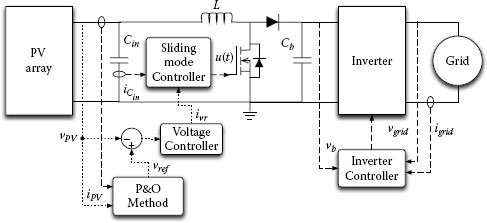
FIGURE 3.24
System scheme based on input capacitor current control.
Two conditions must be fulfilled in order to ensure the sliding mode operation [21]:
(3.56) |
(3.57) |
From the first condition (3.56), also accounting for the characteristic equation of the input capacitor,
(3.58) |
the following condition is obtained:
(3.59) |
From the second sliding mode condition (3.57), also considering that iCin = iPV − iL
(3.60) |
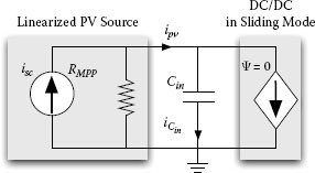
FIGURE 3.25
Small-signal model of the open-loop system.
The analysis of Equation (3.60) can be done by using the linearized model shown in Figure 3.25, wherein the switching converter is represented by a controlled current source whose value is imposed by the SM equation, and the PV generator is given as a Norton model including the photo-induced current source and the differential resistance RMPP, which is calculated in the generator’s operating point. By looking at Figure 3.25, the result is
(3.61) |
As a result, the sliding mode condition given in (3.60) can be thus rewritten as
(3.62) |
In addition, the boost converter model provides the following relationship:
(3.63) |
where vb is the DC/DC converter output voltage and the value u = 1 is used in the MOSFET ON state and the value u = 0 in the OFF state, corresponding to the following driving conditions:
(3.64) |
(3.65) |
In order to obtain the constraints that must be fulfilled to ensure the SM operation, the equivalent control technique [19] can be referred to. The constraints on the inputs and state variables are defined by ensuring that the average control signal ueq fulfills the inequality 0 < ueq < 1. From Equations (3.59)–(3.63) the following equivalent control equation is obtained:
(3.66) |
From (3.55) and (3.60) it can be deduced that the sliding mode equilibrium point is defined by {iPV = iL, ivr = 0}. In (3.66), at the equilibrium point, it is dvPVdt=0; thus the constraints in terms of maximum slope values divrdt and discdt are given by
(3.67) |
According to the superposition principle (divrdt=0) and the linear relation among the short-circuit current and the irradiance isc = Kph, Equation (3.67) gives the constraints for the maximum irradiance variation rate ensuring the sliding mode operation:
(3.68) |
It is worth noting that the lower bound in (3.68) is negative because of the adoption of a boost converter. This means that the larger the converter voltage boosting factor, the faster the negative irradiance variation can be tracked without losing the sliding mode behavior. This might be the case of a step-up DC/DC converter used in PV module-dedicated microinverter applications, in which the low PV module voltage must be boosted up very much, so that the quantity vPV−vbL is deeply negative. Inequality (3.68) reveals that the maximum irradiance variation that can be tracked without losing the sliding mode control depends also on the inductance value; thus L should be properly selected in order to follow the expected irradiance profile and variations, according to the specific applications. For instance, stationary PV power plants will be subjected to slow irradiance variations, while in PV applications dedicated to sustainable mobility fast irradiance variations need to be tracked.
Moreover, putting discdt=0 in (3.67) allows us to take into account the effect of variations on ivr; in particular, the following constraint on divrdt is obtained:
(3.69) |
which again shows that the maximum ivr slope value that can be tracked without missing the sliding mode control depends on the inductor current derivatives in the OFF and ON MOSFET states. In this case, the voltage controller can be designed to fulfill this dynamic constraint.
3.3.2.2 Voltage Controller Design
In sliding mode operation, Equations (3.55) and (3.59) give the time domain relation between the PV voltage and the reference current; thus it allows us to design the voltage compensator. The corresponding transfer function Gv/i(s) between the input capacitor voltage, which is the PV voltage, and the current reference ivr, is
(3.70) |
This expression allows us to point out one of the main features of the proposed control technique. Indeed, it is worth noting that the transfer function (3.70) is not dependent on any PV generator’s parameter, so that the control approach can have the same performances regardless of the environmental conditions and of the PV array type/size connected at the DC/DC converter’s input terminals. This feature is not achievable through classical feedback control. Indeed, as shown in the example of Section 3.1.2 and remarked in [2], the closed-loop system must be designed by considering the worst-case conditions. Furthermore, in the range of validity of the sliding mode conditions, Equation (3.70) is valid without the assumption of the small-signal approximation. Of course the equivalent series resistance (ESR) of the input capacitor changes Equation (3.70) by introducing an additional zero in the loop gain transfer function. In order to avoid that such a zero affects the controller design, capacitors with low ESR, e.g., ceramic capacitor, are recommended for practical implementation. Anyway, the presence of the ESR does not affect the features commented on above.
A PI compensator can be used in the voltage controller loop of Figure 3.24. Given the PI transfer function Gv(s) in (3.71) and the voltage error ev(s) definition (3.72) that compensates the negative sign appearing in (3.70), the closed-loop transfer function Tvp(s) of the system can be expressed by (3.73)
(3.71) |
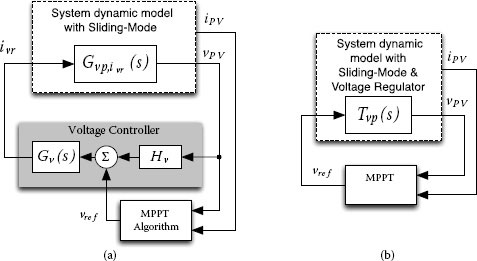
FIGURE 3.26
Dynamic model of the PV system based on input capacitor current SM control. (a) Double-loop representation. (b) Equivalent single-loop representation.
(3.72) |
(3.73) |
Figure 3.26 shows the dynamic models of the system under study. The transfer function Tvp(s) (3.73) allows analysis of the behavior of the whole PV system in the presence of a step perturbation on the PV voltage reference. Thus as shown in the previous chapter, it can be designed by accounting for a desired MPPT speed.
3.3.3 Sliding Mode MPPT Controller: Numerical Example
The SMC on the input capacitor current has been tested by means of PSIM simulation, based on the scheme of Figure 3.24. The parameters of the DC/DC converter are the same as in the previous example and are reported in Table 3.1. The parameters of the PI voltage controller, Gv(s), can be selected by designing the settling time t∈ of the transfer function Tvp(s) in (3.73) according to Equation (2.22). Given the relationships between the settling time t∈ of the closed-loop voltage, the damping (ζ), and the natural frequency (ωn) of the whole PV system, we get
(3.74) |
The comparison of Equation (3.74) with Equation (3.73) gives the following relationships for the parameters of the transfer function Gv(s):
(3.75) |
(3.76) |
From Table 3.1, the nominal switching period is Tsw ≃ 1/fsw0 = 8.3 μs. Choosing tɛ / Tsw = 20, which means imposing a system settling time 20 times greater than the nominal switching period, provides tɛ = 166μs. The second design consideration is related to the damping of the system, which can be settled at ζ = 0.7.
According to the definition of the equivalent time constant, which is τ=1ζωn, the settling time of the closed-loop system can be approximated by tɛ = 4τ when it is assumed that the settling error step response is smaller than 2%. Finally, if the gain of the voltage sensor is Hv = 0.1, then the PI controller transfer function ensuring the desired tɛ and ζ becomes the following:
(3.77) |
In order to verify the stable behavior of the SM on the input capacitor current, the circuit of Figure 3.24 has been tested in the same irradiance condition of the circuit in Figure 3.17 and with the same MPPT parameters, although in this case the P&O algorithm is acting on the voltage reference and not directly on the current reference.
In Figure 3.27 the PV voltage and PV current are shown; an irradiance change from 1000 W/m2 to 900 W/m2 occurs at the time instant t = 0.3 s. The sudden irradiance variations, having an instantaneous effect on the PV short-circuit current, have been correctly tracked, with the system permanently tracking the maximum power point even at the very high rate of irradiance variation that has been considered. Indeed, comparing the voltage behavior with the simulation proposed in Figure 3.22, now no sensible variation in the PV voltage is visible and the system does not crash. Moreover, it is worth noting that also in this case, a bulk voltage oscillation of 127 V has been considered in the scheme of Figure 3.24; the simulation results put into evidence that the large low-frequency oscillations affecting the bulk voltage are almost totally rejected at the PV terminals. Moreover, the upper and lower limits of the irradiance variations dGdt have been calculated by using Equation (3.68) for the numerical example considered in this section. In the considered case, if Kph = 0.008 A · m2/W, it must be
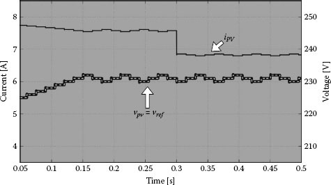
FIGURE 3.27
Simulation of the system of Figure 3.24 using the sliding mode and Gv controllers. MPPT parameters: Δvref = 1 V, Tp = 15 ms.
(3.78) |
In Figure 3.28 an irradiance change from 1000 to 500 W/m2 with a slope of −50Wm2μs has been applied at t = 0.3 s; clearly the system maintains an optimal stable behavior.
Figure 3.29 shows the magnification of the PV voltage in time interval (0.255 s, 0.325 s) in comparison with the bulk voltage. The simulation shows that the PV voltage waveform is free of the 100 Hz oscillations caused by the inverter operation, thus demonstrating that the sliding mode applied to the current of the input capacitor has been able to reject the back propagation of the large oscillations of amplitude Δvb affecting the converter output voltage.
Finally, it is worth noting that in the simulation of Figures 3.27 and 3.28 a nonoptimal Tp MPPT parameter has been used; this is because the intent was to verify the stability of the SMC and not to test the MPPT dynamic performances. Anyway, the tɛ specification also allows us to define the optimal MPPT perturbation period Tp of the P&O algorithms, that is, approximately 1.5 · tɛ. Such a value of Tp ensures that the PV power has reached its steady state when the MPPT controller measures it, thus avoiding the MPPT deception as explained in Section 2.4.1 and in [2, 32]. Thus the case shown in Figure 3.28 has been resimulated by using Tp = 250 μs.
Figure 3.30 puts into evidence the proper design of the P&O parameters leading to a three-point behavior of the PV voltage with an MPPT speed that is about one order of magnitude higher than the case shown in Figure 3.28.
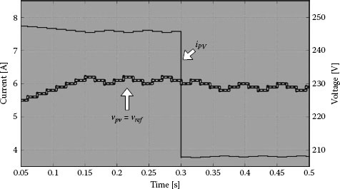
FIGURE 3.28
Simulation of the system of Figure 3.24 using the sliding mode control. MPPT parameters: Δvref = 1 V, Tp = 15 ms.
The same figure shows the waveform of the closed-loop voltage reference vref and the accurate tracking performed by both Gv(s) and the sliding mode controller.
The features listed above make the control strategy shown in Figure 3.24 suitable for all PV applications in which the adoption of electrolytic capacitors at the DC bus must be avoided or wherever an excellent MPPT performance is required.
Moreover, the fast MPPT capability makes the proposed architecture suitable for a large range of applications for which the sudden irradiation changes are very common, e.g., in sustainable mobility and for the PV integration on cars, trucks, buses, ships, and so on.
3.4 Analysis of the MPPT Performances in a Noisy Environment
It is well known that the result of a measurement is only an approximation or estimation of the value of the specific quantity subject to measurement, that is, the measurand, and thus the measure is complete only when it is accompanied by a quantitative statement of the uncertainty affecting it.
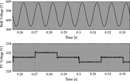
FIGURE 3.29
Bulk voltage and PV voltage.
The uncertainty is the entity that identifies the maximum deviation of a measure with respect to the true value, including stability, precision, resolution, and other factors involved in the measurement and elaboration process.
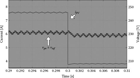
FIGURE 3.30
Simulation of the system of Figure 3.24 using the sliding mode control. MPPT parameters: Δvref = 1 V, Tp = 250 μs.
In whatever MPPT algorithms based on the measurement of the electrical or environmental parameters, the noises and the errors contribute to increase the uncertainty associated to the variable involved in the MPPT, and as a consequence, the decision process can be compromised.
Nonidealities of sensors and sensing amplifiers, analog-to-digital converter (ADC) resolution, and internal arithmetic quantization of the adopted microprocessor (representation of data) can result in measurement uncertainty and bias, which tricks the MPPT algorithm to settle away from the MPP, penalizing both the tracking capability and the steady-state settling point of the PV system. Moreover, the use of switching converters for controlling the operating point of the solar array increases the system noise due to the presence of high-frequency switching ripples.
It is evident that all the above sources of noise and uncertainty should be taken into account in the evaluation of the MPPT performances in order to identify possible solutions to mitigate their effect.
To date, there is not so much in scientific literature that specifically addresses the effect of noise on the MPPT algorithm; in [33] a comparison of convergence characteristics of different search strategies in the presence of noise is discussed in detail. In [34] the behavior of MPPT in a noisy environment has been analyzed by using a probabilistic model based on the statistical characteristics of the noise signal. Analysis presented therein highlights that noise in the voltage measurement shifts the settling point of the MPPT to the right-hand side of the characteristics curve, while noise in the current measurement reduces the MPPT tracking speed. Enhanced signal filtering and larger perturbations are found to be effective in building the system immunity to noise.
In this section, the behavior of the MPPT algorithms in a noisy environment will be analyzed by means of a similar approach. The method adopted exploits the concept of the uncertainty of a measure to characterize different types of errors. Indeed, being that uncertainty is a cumulative entity, it can be used for evaluating the global effect of errors introduced in the measurement and elaboration process and of noise sources on the MPPT performances.
If the noise sources, which are distributed in different places of the PV system, are expressed by means of an uncertainty value (u) with respect to the corresponding true value of the variable, the global uncertainty on a variable that is not directly measured can be estimated by applying the law of propagation of uncertainty [35].
Indeed, if a measurand y is not directly measured (e.g., the power in the MPPT algorithm), but rather is determined from N other quantities x1, x2, …, xN through a functional relation f,
(3.79) |
then the combined standard uncertainty of the measurement y, designated by uy, is given by
(3.80) |
where it has been assumed that all the input quantities xi are independent.
In Figure 3.31 a typical MPPT converter is shown where several sources of uncertainty have been highlighted in grey.
It is worth noting that only the most significant noise sources have been reported; they have been indicated with the following uncertainty components: the switching ripple noise (uSwitching), the measurement errors (uv, ui), the errors in numerical elaboration (uE), and the output voltage noise (uv0). Depending on the type of uncertainty (errors in the measurement, noise coming from the switching converter), different actions must be performed on the system in order to mitigate their effect.
The method can be easily generalized for estimating the effect of other types of uncertainty and for other MPPT algorithms.
3.4.1 Noise Attenuation by Using Low-Pass Filters
Processing the measured signals by means of a low-pass filter (LPF) is the first method for attenuating the effects of the noise. This method, however, should be applied carefully in order to avoid suppressing useful information, destabilizing the MPPT control loop, or sacrificing its promptness. Indeed, although the LPF can be designed to attenuate the amplitude of any noise coming from the switching converter, its intrinsic phase delay may degrade the tracking capability of the MPPT algorithm.
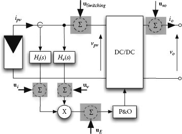
FIGURE 3.31
Uncertainty distribution in a P&O MPPT switching converter.
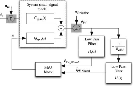
FIGURE 3.32
Effect of the LPF on the MPPT dynamics.
The scheme shown in Figure 3.32 is an extension of the scheme shown in Figure 3.4 in which the effect of the output voltage noise uvo and the switching noise uswitching have been highlighted. The LPF filters have also been included. This new scheme is useful for analyzing the MPPT dynamic behavior and for evaluating the right time interval Tp between two consecutive perturbations in a perturbative approach in more realistic operating conditions of the PV system. If we suppose that both LPFs processing the signals related to the PV voltage and the PV current have the same dynamic characteristics, then their effects on the P&O dynamics can be accounted for by considering the LPF on the PV voltage only. The equation (2.22), used to design the value of Tp in the ideal case, must be suitably corrected by accounting for the effect of the whole transfer function Gvp,x(s) · Hv(s), thus including the LPF transfer function Hv(s). It is worth noting that the Gvp,x(s) transfer function includes the whole dynamic effect between the perturbed variable x and the PV voltage.
The minimum Tp value depends on the system dynamic and also on the used LPF. A too low cutoff frequency of Hv(s) might be unacceptable if a fast MPPT is required. Moreover, if the LPF is digitally implemented, the sampling time and the elaboration time are additional time delays and must be taken into account in the evaluation of Tp.
The LPF is effective for removing high-frequency noise because if its dynamic is faster than the converter dynamics it does not affect the choice of Tp.
The uncertainty (uvPV) on the PV voltage, which accounts for all the possible noises affecting this variable, is related to uSwitching as follows:
(3.81) |
where Hv(ωs) is the gain of the PV voltage sensor evaluated at the switching frequency ωs.
A well-designed LPF is obtained if |Hv(ωs| ≃ 0. On the basis of the assumption given before, the PV current is also not affected by the switching noise.
The noise uvo is in the low-frequency range, so that the LPF does not attenuate it and its effect in the decision process of the MPPT algorithm must be taken into account. It can be accounted for as a further contribution to the uncertainty affecting the PV voltage uvPV; thus
(3.82) |
where |Gvp,vo(ω)| is the magnitude of the output-to-input transfer function evaluated at the frequency of the noise and Hv(ω) is the gain of the PV voltage sensor evaluated at the same frequency. This value will be accounted for in whichever expression involving the PV voltage variable. For example, in the estimation of the PV voltage variation between two consecutive P&O perturbations, it is
(3.83) |
From the propagation of uncertainty it results that
(3.84) |
where ΔVPV is the PV voltage variation in an error-free environment, while ΔVPV,uupv is the PV voltage variation corrected by an uncertainty due to the voltage noise uvo. The difference between (3.84) and (3.16) is that the peak-to-peak ΔVo output oscillation is now correctly represented by the double of the uncertainty uvo. The new formalization is more suitable for including this effect in the cumulative uncertainty of ΔPPV in which other noise sources can be accounted for.
The total uncertainty on the measured values of vPV and iPV is useful for estimating the optimal P&O step perturbation.
3.4.2 Error Compensation by Increasing the Step Perturbation
As explained in the previous section, not all of the uncertainty sources affecting the electrical variables on which the MPPT strategy is based can be removed or attenuated, so that they can affect the MPPT operation. In order to avoid any wrong decision in tracking the MPP, or to reduce at least the probability of their occurrence, the presence of uncertainty can be compensated by increasing the step amplitude of the P&O perturbation. This approach, in analogy with what is done in telecommunication systems, corresponds to an increase of the signal-to-noise ratio (SNR). Such a solution must be carefully used only if any other possible method has been used in order to improve the results, because, as already remarked, an increase of the step amplitude reduces the MPPT efficiency, so that the error compensation is paid with a loss of energy. In this section the relations among the various uncertainty sources and the MPPT parameters have been discussed in order to identify designing rules for selecting the values of the other parameters of the PV system that assure, whenever possible, the same P&O step amplitude of the system without uncertainties.
If we refer to Figure 3.31 and suppose that the errors of the measurement stage are included in the uncertainty values ui and uv of the measured PV current and PV voltage, then it will be
(3.85) |
where im and νm are the measurement of the current and voltage while ipν and νpν are the true values of the current and voltage of the PV field. The scaling factors of the current and voltage sensors, Hi and Hv, are also taken into account. It is worth noting that the scaling factors are the static gains of the LPF transfer functions Hi(s) and Hv(s).
Inverting the previous equations with respect to iPV, vPV and considering the error-free measurements provide
(3.86) |
The uncertainty propagation law (3.80) applied to the PPV expression yields
(3.87) |
Accounting for additional uncertainty uE due to the elaboration process, in terms of PV voltage and current, provides
(3.88) |
so that the PV power can be expressed as
(3.89) |
Equation (3.88) is used to find the best compromise among the maximum value of the uncertainties ui, uv affecting the measured signals, the voltage and current gains Hv, Hi, and the numerical resolution uE of the elaboration process that minimize the uncertainty uPPV on the PV power variation.
The P&O algorithm is based on the measurement of the power variations due to two consecutive perturbations, so that applying the uncertainty propagation law yields
(3.90) |
where ΔPPV,UΔP is the power variation in presence of uncertainty, Pk+1PV and PkPV are the power in two consecutive steps of the MPPT perturbations in presence of uncertainty, while ΔPPV is the power variation in the ideal noiseless conditions. As a consequence the uncertainty on ΔPPV will be uΔp = uPpv. In the P&O decision process ΔPPV,uΔP allows us to establish the sign of the next perturbation; thus in order to avoid wrong behavior due to the uncertainty, the sign of ΔPPV,uΔP must be the same as that of ΔPPV which is the real power variation of the PV field. This condition is fulfilled if
(3.91) |
On the other side, ΔPPV itself is a combination of the PV power variations due to the P&O step perturbation, irradiance variation, and other uncertainty sources (e.g., output voltage oscillation). By means of the same procedure used for obtaining (2.32), taking into account the uncertainty, it results that
(3.92) |
where ΔVPV,UVPV is the voltage variation in presence of uncertainty and it is related to the other parameters by means of (3.84).
Thus in order to estimate the right perturbation amplitude Δx, (2.23) must be modified as follows:
(3.93) |
where ΔPx and ΔPG have the same meaning of the parameters appearing in (2.23).
Finally, combining (2.32)–(2.35) with (3.84), (3.88), and (3.93), evaluated in the MPP, provides
Δx>1|G0|√VMPP⋅Kph⋅|˙G|⋅Tp+2⋅√v2PV(uiHi)2+i2PV(uvHv)2+2uE(H⋅VMPP+1RMPP) +2⋅|Gvp,vo(ω)||G0|⋅uvo |
(3.94) |
The lower uv0, ui, uv, and uE, the lower the power uncertainty, so that a right choice of the sensors, LPF parameters, CPU, and switching converter transfer functions allows minimization of the error in the estimation of the PV power and, consequently, reduction of the optimal value of Δx in the P&O algorithm.
In practice, (3.88) and the dynamic information taken from the Hv(s), Hi(s) transfer functions give the design criteria for designing the measurement system in a P&O-based MPPT controller in the best way. uE, instead, gives an idea of the CPU performances required for realizing a well-designed P&O MPPT.
3.4.3 ADC Quantization Error in the P&O Algorithm: Numerical Example
In order to show the way in which (3.94) is used, the contribution of the measurement errors uv, ui in the increase of the step amplitude of a digitally implemented P&O MPPT algorithm is described. Table 3.2 gives the parameters of the PV field and of the boost converter used for evaluating the P&O step perturbation.
For an ideal noise-free system (uvo = ui = uvuE = 0), the use of (3.94) gives
(3.95) |
The uncertainty components are added one at the time so that the contribution of each one of them to the increase of Δx is shown. In the measurement stage the uncertainty due to the quantization errors introduced by the ADCs is accounted for. According to [35], some additional error sources should be accounted for, but the modeling of such terms is out of the scope of this book. It is assumed that the uncertainty is directly related to the last significant bit (LSB) and to ADC voltage resolution, so that
Parameters of the PV Field and of the Boost Converter
PV Array |
Values at 300 W/m2 and T = 35°C |
MPP voltage VMPP |
356 V |
MPP current IMPP |
2.22 A |
MPP resistance RMPP |
161 Ω |
HMPP |
1.157∙10−4 A/V2 |
Coefficient of the photo-induced current Kph |
83 mA∙m2/W |
PV Measurable Parameters |
Maximum Values |
PV field current IPV,max |
10 A |
PV field voltage VPV,max |
600 V |
MPPT Design Parameters |
Nominal Values |
Irradiance variation |
100 W/m2/s |
P&O time interval TpG |
2 ms |
Boost output voltage Vo = Go |
600 V |
Output voltage oscillation Δ V0 = uvo |
0 V |
(3.96) |
where VFS is the full-scale input voltage and N is the number of bits of the ADCs. Moreover, in order to map the PV voltage and current in the VFS range, the Hv and Hi scaling factors must be chosen according to the following equations:
(3.97) |
If N = 10 bits and VFS = 5 V are adopted, which are typical values for the ADC parameters from Table 3.2, it results that
(3.98) |
Such values are put in (3.94), so that the new value for Δx must fulfill the following constraint:
(3.99) |
which is almost three times greater than the value in noiseless conditions given in (3.95).
Of course this is the condition in which the quantization errors, introduced in the measurement process, produce a wrong decision in the MPPT algorithm with a probability almost zero. If a lower level of confidence in the P&O decision is accepted, Δx can be reduced progressively.
Alternatively, in order to improve the MPPT performances as much as possible, the optimal Δx can be reduced by using different ADCs. Table 3.3 shows the results for three ADCs characterized by different numbers of bits but with the same VFS. Based on (3.88), it is also possible to evaluate separately the effect of uv and ui on the PV power estimation; this can be useful for identifying the channel that is more sensible to quantization error.
Table 3.3 shows clearly which is the minimum number of bits in the ADC that makes the quantization error negligible. It is worth noting that the uncertainty coming from the two measurement channels can be significantly different. Indeed, in Table 3.3, such a difference has been highlighted by showing the values of the power uncertainty due to the two channels separately. In particular, ΔPUi is the increase in the power variation due to uncertainty on the measurement of the PV current (ui), and ΔPUv is the increase in the power variation due to uncertainty on the measurement of the PV voltage (uv). The sensibility of the MPPT performances with respect to quantization error is such a critical aspect that some manufacturers produce ADC with high resolution specifically designed for power monitoring in PV application [36]. Alternatively, digital processing combined with multiple sampling of PV variables can be used for increasing fictitiously the equivalent number of the ADC bit [37]. In conclusion, it is possible to state that the action concerning the minimization of uncertainty must be focused on the noise sources that influence more heavily the decision process of the MPPT. Equation (3.94) shows clearly this dependency for the P&O algorithm.
ADC Resolution on the MPPT Performances
ADC 10 Bit |
ADC 16 Bit |
ADC 20 Bit |
|
ui, uv |
2.4 mV |
38 μV |
2.4 μV |
ΔPu |
≃3.5 W |
≃56 mW |
≃3.4 mW |
ΔPu |
≃1 W |
≃17 mW |
≃1 mW |
Δx |
0.0157 |
0.0062 |
0.0059 |
1. S. B. Kjær. Design and control of an inverter for photovoltaic applications. PhD thesis, Aalborg University, Denmark Institute of Energy Technology, January 2005.
2. N. Femia, G. Petrone, G. Spagnuolo, and M. Vitelli. A technique for improving P&O MPPT performances of double stage grid-connected photovoltaic systems. IEEE Transactions on Industrial Electronics, 56(11):4473–4482, 2009.
3. R.-J. Wai and C.-Y. Lin. Active low-frequency ripple control for clean-energy power-conditioning mechanism. IEEE Transactions on Industrial Electronics, 57:3780–3792, 2010.
4. R. S. Gemmen. Analysis for the effect of inverter ripple current on fuel cell operating condition. Journal of Fluids Engineering, 125(3):576–585, 2003.
5. C. Liu and J.-S. Lai. Low frequency current ripple reduction technique with active control in a fuel cell power system with inverter load. IEEE Transactions on Power Electronics, 22(4):1429–1436, 2007.
6. S. K. Mazumder, R.K. Burra, and K. Acharya. A ripple-mitigating and energy-efficient fuel cell power-conditioning system. IEEE Transactions on Power Electronics, 22(4):1437–1452, 2007.
7. K. Fukushima, I. Norigoe, M. Shoyama, T. Ninomiya, Y. Harada, and K. Tsukakoshi. Input current-ripple consideration for the pulse-link DC-AC converter for fuel cells by small series LC circuit. In Twenty-Fourth Annual IEEE Applied Power Electronics Conference and Exposition (APEC 2009), February 2009, pp. 447–451.
8. J.-I. Itoh and F. Hayashi. Ripple current reduction of a fuel cell for a single-phase isolated converter using a dc active filter with a center tap. In Twenty-Fourth Annual IEEE Applied Power Electronics Conference and Exposition (APEC 2009), February 2009, pp. 1813–1818.
9. J.-M. Kwon, E.-H. Kim, B.-H. Kwon, and K.-H. Nam. High-efficiency fuel cell power conditioning system with input current ripple reduction. IEEE Transactions on Industrial Electronics, 56(3):826–834, 2009.
10. E. Mamarelis, C.A. Ramos-Paja, G. Petrone, G. Spagnuolo, M. Vitelli, and R. Giral. FPGA-based controller for mitigation of the 100 Hz oscillation in grid connected PV systems. In 2010 IEEE International Conference on Industrial Technology (ICIT), March 2010, pp. 925–930.
11. T. Brekken, N. Bhiwapurkar, M. Rathi, N. Mohan, C. Henze, and L.R. Moumneh. Utility-connected power converter for maximizing power transfer from a photovoltaic source while drawing ripple-free current. In 2002 IEEE 33rd Annual Power Electronics Specialists Conference, 2002, vol. 3, pp. 1518–1522.
12. R. W. Erikson and D. Maksimovic. Fundamentals of power electronics. 2nd ed. Kluwer Academic Publishers, Norwell, MA, 2000.
13. L. Castanier and S. Silvestre. Modelling photovoltaic systems using pspice. vol. 1. John Wiley & Sons, West Sussex, UK, 2002.
14. V. Salas, E. Olìas, A. Barrado, and A. Làzaro. Review of the maximum power point tracking algorithms for stand-alone photovoltaic systems. Solar Energy Materials and Solar Cells, 90:1555–1576, 2006.
15. J. P. Gaubert, R. Kadri, and G. Champenois. An improved maximum power point tracking for photovoltaic grid-connected inverter based on voltage-oriented control. IEEE Transactions on Industrial Electronics, 58(1):66–75, 2011.
16. O. Lopez-Lapena, M.T. Penella, and M. Gasulla. A new MPPT method for low-power solar energy harvesting. IEEE Transactions on Industrial Electronics, 57(9):3129–3138, 2010.
17. O. Lopez-Lapena, M. Penella, and M. Gasulla. A close-loop maximum power point tracker for sub-watt photovoltaic panels. IEEE Transactions on Industrial Electronics, PP(99):1, 2011.
18. Y. Xue, L. Chang, S.B. Kjær, J. Bordonau, and T. Shimizu. Topologies of single-phase inverters for small distributed power generators: An overview. IEEE Transactions on Power Electronics, 19(5):1305–1314, 2004.
19. H. Sira-Ramirez. Sliding motions in bilinear switched networks. IEEE Transactions on Circuits and Systems, 34(8):919–933, 1987.
20. L. Rossetto, G. Spiazzi, P. Tenti, B. Fabiano, and C. Licitra. Fast-response high-quality rectifier with sliding mode control. IEEE Transactions on Power Electronics, 9(2):146–152, 1994.
21. S.-C. Tan, Y.M. Lai, and C.K. Tse. General design issues of sliding-mode controllers in dc dc converters. IEEE Transactions on Industrial Electronics, 55(3):1160–1174, 2008.
22 M. A. Sofla and G.B. Gharehpetian. Dynamic performance enhancement of microgrids by advanced sliding mode controller. International Journal of Electrical Power and Energy Systems, 33(1):1–7, 2011.
23. J. Fernandez-Vargas and G. Ledwich. Variable structure control for power systems stabilization. International Journal of Electrical Power and Energy Systems, 32(2):101–107, 2010.
24. R.-J. Wai, W.-H. Wang, and C.-Y. Lin. High-performance stand-alone photovoltaic generation system. IEEE Transactions on Industrial Electronics, 55(1):240–250, 2008.
25. R.-J. Wai and W.-H. Wang. Grid-connected photovoltaic generation system. IEEE Transactions on Circuits and Systems I: Regular Papers, 55(3):953–964, 2008.
26. Y.-K. Lo, S.-C. Yen, and C.-Y. Lin. A high-efficiency AC-to-DC adaptor with a low standby power consumption. IEEE Transactions on Industrial Electronics, 55(2):963–965, 2008.
27. Linear Company. Burst mode in Linear products. LTC3458. http://cds.linear.com/docs/datasheet/3442fa.pdf.
28. Powersim. Power electronics simulation software, 2008. http://www.power-sys.fr/psimpresent.php.
29. G. Spagnuolo, G. Petrone, M. Vitelli, J. Calvente, C. Ramos-Paja, R. Giral, E. Mamarelis, and E. Bianconi. A fast current-based MPPT technique employing sliding mode control. IEEE Transactions on Industrial Electronics, PP(99):1, 2012.
30. E. Bianconi, J. Calvente, R. Giral, G. Petrone, C.A. Ramos-Paja, G. Spagnuolo, and M. Vitelli. A fast current-based MPPT technique based on sliding mode control. In 2011 IEEE International Symposium on Industrial Electronics (ISIE), June 2011, pp. 59–64.
31. E. Bianconi, J. Calvente, R. Giral, G. Petrone, C.A. Ramos-Paja, G. Spagnuolo, and M. Vitelli. Improving the perturb and observe maximum power point tracking by using sliding mode control. In 2011 IEEE International Symposium on Industrial Electronics (ISIE), June 2011, pp. 310–315.
32. N. Femia, G. Petrone, G. Spagnuolo, and M. Vitelli. Optimization of perturb and observe maximum power point tracking method. IEEE Transactions on Power Electronics, 20(4):963–973, 2005.
33. D. Arnold and H.-G. Beyer. A comparison of evolution strategies with other direct search methods in the presence of noise. Computational Optimization and Applications, 24:135–159, 2003. 10.1023/A:1021810301763.
34. H. Al-Atrash, I. Batarseh, and K. Rustom. Effect of measurement noise and bias on hill-climbing MPPT algorithms. IEEE Transactions on Aerospace and Electronic Systems, 46(2):745–760, 2010.
35. JCGM/WG 1. Evaluation of measurement data—Guide to the expression of uncertainty in measurement. Working Group 1 of the Joint Committee for Guides in Metrology, September 2008.
36. Texas Instruments. High-resolution analog-to-digital converter—ads1282. http://www.ti.com/lit/ds/symlink/ads1282.pdf, 2012.
37. E. Balestrieri, P. Daponte, and S. Rapuano. A state of the art on ADC error compensation methods. IEEE Transactions on Instrumentation and Measurement, 54(4):1388–1394, 2005.