
In this chapter we take a closer look at four multicore designs from some of the computer industry's leading chip manufacturers:
The AMD Multicore Opteron
The Sun UltraSparc T1
The IBM Cell Broadband Engine (CBE)
The Intel Core 2 Duo
Each of these vendors approaches the Chip Multiprocessor (CMP) differently. Their approaches to multicore design are implemented effectively with each design having its advantages, strengths, and weaknesses in comparison to the other designs. We will use these designs for all of the examples in this book. The program examples in this book have been compiled and executed on one or more of these multicore processor designs. In this chapter, we introduce you to the basics of each design, and throughout the book we fill in the necessary detail as it pertains to multicore application development and design.
In many mass market software applications, the differences among hardware implementations are abstracted away because often one of the primary design goals is to make the software compatible with as many different hardware platforms as possible. So there is a conscious effort to avoid platform-specific features. In these scenarios, the software designer and developer appropriately rely on the operating system to hide any platform differences that the applications might encounter. The developers move happily and blissfully through the development process without the burden of having to worry about hardware-specific issues. This is a good thing! One of the primary jobs of the operating system is to hide and manage hardware details. And this approach works for an entire class of mass market or wide vertical market applications.
However, not every kind of software developer is so lucky. For example, those developing high-transaction database servers, web servers, application servers, hardware-intensive game engines, compilers, operating system kernels, device drivers, and high-performance scientific modeling and visualization software are practically forced to look for and exploit platform features that will make their applications acceptable to the end user. For this class of developer, familiarity with a specific processor or family of processors is a prerequisite for effective software development. Table 2-1 lists the types of applications that can require platform-specific optimization.
Table 2.1. Table 2-1
Software Type | Developer Type |
|---|---|
High transaction software servers
|
|
Kernels |
|
Game engines |
|
Device drivers |
|
Large-scale matrix and vector computations |
|
Compilers |
|
Database engines |
|
High-definition computer animation |
|
Scientific visualization modeling |
|
In Table 2-1, we have also listed some of the types of developers involved with these types of applications. System programmers, graphics programmers, application developers, and software engineers who are trying to optimize the performance of a piece of software need to be aware of the capabilities of the target platform. In the cases where cross-platform portability is the primary consideration, platform-specific optimizations should be approached with caution. In other cases, cross-platform compatibility is not a concern, and the best performance on the target platform is the goal. In these situations the more the developer knows about the target processor or family of processors the better.
In this book, we look at top-down and bottom-up approaches to multiprocessor application design and implementation. To take advantage of bottom-up approaches to multiprocessor programming requires a fundamental understanding of the CMP architecture, the operating system's support for multithreading and multiprocessing, and the C/C++ compiler for the target platform. In Chapter 4, we take a closer look at operating system and compiler support for multicore development. But first here in this chapter we explore the four effective multicore designs we mentioned at the start of the chapter. Table 2-2 shows a comparison of the Opteron, UltraSparc T1, CBE, and Core 2 Duo processors.
The dual core Opteron is the entry level into AMD's multicore processor line. The dual core Opteron is the most basic configuration, and it captures AMD's fundamental approach to multicore architectures. The Opteron is source and binary code compatible with Intel's family of processors, that is, applications written for the Intel processors can compile and execute on Opterons. Figure 2-1 shows a simple block diagram of a dual core Opteron.
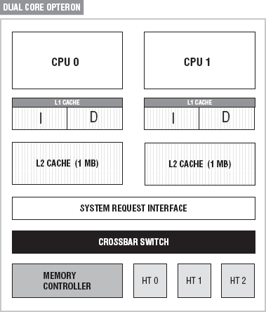
The dual core Opteron consists of two AMD 64 processors, two sets of level 1 (L1) cache, two sets of level 2 (L2) cache, a System Request Interface (SRI), a crossbar switch, a memory controller, and HyperTransport technology. One of the key architectural differences between the Opteron and other designs is AMD's Direct Connect Architecture (DCA) with HyperTransport technology. The Direct Connect Architecture determines how the CPUs communicate with memory and other I/O devices.
To understand the value of AMD's approach to subsystem communication, it's important to remember what part bus technology plays in the processor architecture. See the section "The Bus Connection" in Chapter 1 for more information on bus technology.
The Opteron processor moves away from this bus-based architecture. It uses a Direct Connect Architecture (DCA) in conjunction with HyperTransport (HT) technology to avoid some of the performance bottlenecks of the basic Front Side Bus (FSB), Back Side Bus (BSB), and Peripheral Component Interconnect (PCI) configurations.
The DCA is a point-to-point connection scheme. It does not use the FSB. Instead the processors, memory controller, and I/O are directly connected to the CPU. This dedicated link approach avoids the potential performance problems of the bus-based communication between the CPU and the memory controller. Also because the links are dedicated — that is, each core is directly connected to its own memory controller and has direct links to the I/O memory controller — contention issues are bypassed.
The HyperTransport Consortium defines HyperTransport as a high-speed, low-latency, point-to-point link designed to increase the communication speed between integrated circuits in computers, servers, embedded systems, and networking and telecommunications equipment. According to the HyperTransport Consortium, HT is designed to:
Provide significantly more bandwidth
Use low-latency responses and low pin counts
Maintain compatibility with legacy buses while being extensible to new network architecture buses
Appear transparent to operating systems and have little impact on peripheral drivers
The Opteron uses HT as a chip-to-chip interconnection between CPU and the I/O. The components connected with HT are connected in a peer-to-peer fashion and are, therefore, able to communicate with each other directly without the need of data buses. At peak throughput the HT provides 12.8 GB/s per link. The Opteron configuration comes configured with up four HT Links. I/O devices and buses such as PCI-E, AGP, PCI-X, and PCI connect to the system over HT Links. The PCIs are I/O buses, and the AGP is a direct graphics connection. The PCI, PCI-E, and AGP are used to connect the system to peripheral devices. Besides improving the connections between the processors and I/O, HT is also used to facilitate a direct connection between the processors on the Opteron. Multicore communication on the Opteron is enhanced by using HT.
The System Request Interface (SRI) contains the system address map and maps memory ranges to nodes. If the memory access is to local memory, then a map lookup in the SRI sends it to the memory controller for the appropriate processor. If the memory access is not local (off chip), then a routing table lookup sends it to a HT port. For more see [Hughes, Conway, 2007 IEEE]. Figure 2-2 shows a logic layout of the crossbar.
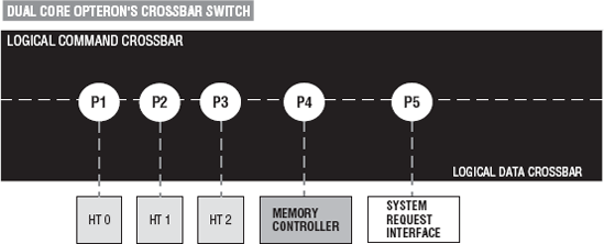
The crossbar has five ports: memory controller, SRI, and three HTs. The crossbar switch processing is logically separated into command header packet processing and data header packet processing. Logically, part of the crossbar is dedicated to command packet routing, and the other part is dedicated to data packet routing.
Opteron has a Non-Uniform Memory Access (NUMA) architecture. In this architecture, each processor has access to its own fast local memory through the processor's on-chip memory controller. NUMA architecture has a distributed but shared memory architecture. This is in contrast to the Uniform Memory Access (UMA) architecture. Figure 2-3 shows a simplified overview of a UMA architecture.
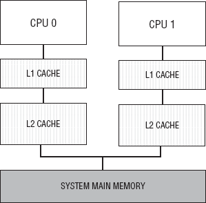
Notice in Figure 2-3 that the processors share a single memory. Each of the access times for each processor is symmetric with the other. The processor configuration in Figure 2-3 is often called a symmetric (shared-memory) multiprocessor (SMP). This arises from the fact that all processors have a uniform latency from memory even if the memory is organized into multiple banks [Hennessy, Patterson, 2007]. The single main memory and the uniform access time in the SMP makes it easier to implement than it NUMA counterpart. Also the notion of a shared address space is more straightforward in the UMA architecture because there is only one main system memory to consider.
In contrast, Figure 2-4 shows a simplified overview of a NUMA architecture.
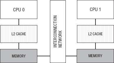
The NUMA is a distributed shared memory (DSM) architecture. Notice in Figure 2-4 that each processor has its own block memory, but each block of memory shares a single address space. That is, the same physical address on two processors refers to the same location in memory [Hennessy, Patterson, 2007]. In both cases, the UMA and the NUMA configurations, the processors share address space. However, in the NUMA architecture the address space is shared from a logical viewpoint, and in the UMA configuration the processors physically share the same block of memory. The SMP architecture is satisfactory for smaller configurations, but once the number of processors starts to increase, the single memory controller can become a bottleneck and, therefore, degrade overall system performance. The NUMA architecture, on the other hand, scales nicely because each processor has its own memory controller.
If you look at the configuration in Figure 2-4 as a simplified Opteron configuration, then the network interconnection is accomplished by the Opteron HyperTransport technology. Using the HyperTransport technology, the CPUs are directly connected to each other and the I/O is directly connected to the CPU. This ultimately gives you a performance gain over the SMP configuration.
The dual core Opteron supports two levels of cache. L1 cache can be logically divided between I-Cache (for instructions) and D-Cache (for data). Each core has its own L1 cache. Each core in the Opteron also has its own 1MB L2 cache between the processor and main system memory.
The UltraSparc T1 is an eight-core CMP and has support for chip-level multithreading (CMT). Each core is capable of running four threads. This is also sometimes referred to as hyperthreaded. The CMT of the UltraSparc T1 means that the T1 can handle up to 32 hardware threads. What does this mean for the software developer? Eight cores with four threads presents itself to an application as 32 logical processors. Listing 2-1 contains code that can be used to see how many processors are apparently available to the operating system (without special compilers and so on).
Example 2.1. Listing 2-1
// Listing 2-1
// uses sysconf() function to determine how many
// processors are available to the OS.

using namespace std;
#include <unistd.h>
#include <iostream>

int main(int argc,char *argv[])
{
   cout < < sysconf(_SC_NPROCESSORS_CONF) < < endl;
   return(0);
}
When appropriate, in this book listings are accompanied by a program profile stating the environment platform for the program. Anyone wishing to run code for a noncompliant OS needs to use the POSIX-compliant features for that OS.
This program uses sysconf() function to determine how many processors are available to the operating system.
None
When this program is executed on a T1, it prints 32. The sysconf() function provides a method for an application to get values for system limits or variables. In this case the _SC_NPROCESSORS_CONF argument asks for the number of processors configured. The_SC NPROCESSORS_MAX argument can be used to get the maximum number of processors supported. The UltraSparc T1 offers the most on-chip threads of the architectures that we discuss in the book. Each of the eight cores equates to a 64-bit execution pipeline capable of running four threads. Figure 2-5 contains a functional overview of an UltraSparc T1 multiprocessor.
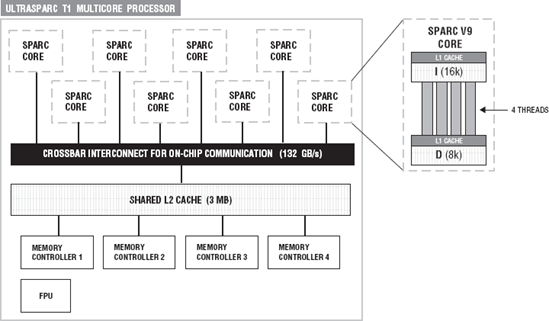
The T1 consists of eight Sparc V9 cores. The V9 cores are 64-bit technology. Each core has L1 cache. Notice in Figure 2-5 that there is a 16K L1 instruction cache and an 8K L1 data cache. The eight cores all share a single floating-point unit (FPU). Figure 2-5 shows the access path of the L2 cache and the eight cores. The four threads share L2 cache. Each core has a six-stage pipeline:
Fetch
Thread selection
Decode
Execute
Memory access
Write back
Notice in Figure 2-5 that the cores and the L2 cache are connected through the cross-switch or crossbar. The crossbar has 132 GB/s bandwidth for on chip communications. The crossbar has been optimized for L2 cache-to-core communication and for core-to-L2 cache communication. The FPU, the four banks of L2 cache, the I/O bridges, and the cores all communicate through the crossbar. Basically the crossbar acts as the mediator, allowing the components of the T1 to communicate to each other.
The UltraSparc T1 has four separate memory controllers. Each controller is connected to one bank of L2 cache. The L2 cache is divided on the T1 into four banks. The T1 can support up to 128GB of RAM.
We introduce the architecture of the UltraSparc T1 to contrast it with that of the AMD Opteron, IBM Cell Broadband architecture, and the Intel Core 2 Duo. While each of these architectures is multicore, the different implementations are dramatic. From the highest level, an application designed to take advantage of multicore will see them all as a collection of two or more processors. However, from an optimization point of view, there is much more to take into consideration. Two of the most commonly used compilers for the UltraSparc T1 are the Sun C/C++ compiler (part of Sun Studio) and the GNU gcc, the standard open source C/C++ compiler. While Sun's compilers obviously have the best support for their processors, GNU gcc has a great deal of support for T1, with options that take advantage of threads, loop unrolling, vector operations, branch prediction, and Sparc-specific platform options. Virtually all of the program examples in this book have been compiled and executed on a SunFire 2000 with an eight-core T1 processor. Look at the program profiles for the program listings, and you will see which compiler switches we explored for the T1.
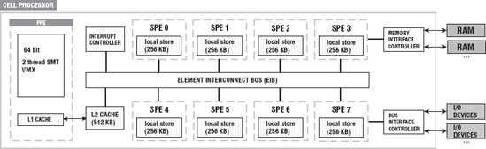
The CBE is a heterogeneous multicore chip. It is a heterogeneous architecture because it consists of two different types of processors: PowerPC Processing Element (PPE) and Synergistic Processor Element (SPE). The CBE has one PPE and eight SPEs, one high-speed memory controller, one high-bandwidth element interconnect bus, high-speed memory, and I/O interfaces all integrated on-chip. This makes it a kind of hybird nine-core processor. Figure 2-6 shows an overview of the CBE processor.
Most of the common CMPs have homogeneous processors, that is, ones with the same instruction set. The processors on the CBE have two different instruction sets. Although each of the processor elements has been optimized for certain types of operations, both types of elements can be used for general-purpose computing.
The first element in the Cell processor is a 64-bit PowerPC processor. This element complies fully with the 64-bit PowerPC architecture and can execute either 32-bit or 64-bit operating systems and applications.
The second type of processor element is the SPE. The SPEs have been optimized for running Single Instruction Multiple Data (SIMD) applications.
Although there are several commercial scientific uses of the CBE, its most common use is as the processor for Sony's Playstation 3.
We selected the CBE as one of our four effective multicore architecture designs because it is able to deliver so much performance in a Linux environment. The Playstation 3 is a flexible device and comes with ready-to-install Linux. Currently, there is a Fedora and a Yellow Dog distribution of Linux for the CBE. The low cost of the Playstation 3 (PS3) brings heterogeneous multicore application development into reach of virtually any software developer. The PPE element and the SPEs can be programmed using the standard GNU gcc compiler. There is a CBE SDK available for downloading from IBM that includes tools necessary to compile the SPE code. Basically, the SPE code is compiled separately and then linked with the PPE code to form a single execution unit. The PPE and SPEs act cooperatively, with both bringing specialties to the table. Typically, the SPEs use the PPE to run the operating system code and in most applications the main or top-level thread. The PPE (the general purpose processor) uses the SPEs as the application's high-performance workhorse. The SPEs have good support for SIMD operations, computer-intensive applications, and vector type operations. When you execute the code from Listing 2-1 on the CBE, the number printed to the console is 2. This is because the SPEs are directly accessible. The 2 represents the fact that the PPE is a CMT; it is a dual thread processor. So in the right configuration, you can have multiple logical processors (including the SPEs) available in a CBE configuration. The heterogeneous architecture also makes for some interesting design choices.
While standard POSIX threads (pthreads) and process management can be used with the PPE element, the SPE has to be programmed using the thread library that's available as part of the CBE SDK. The good news is the SPE thread calls are designed to be compatible with pthreads and require no learning curve for developers who are familiar with the pthread library.
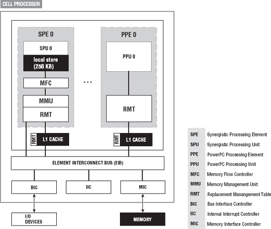
The PPE accesses memory differently than the SPEs. Although there is only a single memory flow controller, the CBE avoids the normal single bus bottleneck potentials because the SPEs each have their own local memory. Figure 2-7 shows the memory configurations for the PPE and the SPE.
The SPE configuration is where most of the savings come in. The SPE has a three-level memory access. It uses its local store, register files, and direct memory access (DMA) transfers to main memory. This three-tier memory architecture allows programmers to schedule simultaneous data and code transfers. The CBE processor can support up to 128 simultaneous transfers between the SPE local stores and main storage. Although the SPE is optimized for SIMD type operations, the PPE has support for parallel vector/SIMD operations as well.
Hidden from the Operating System
The CBE is a good example of a multicore that must be directly addressed to get the maximum performance from it. The standard Linux system calls can see the dual threads of the PPE but are not fully aware of the SPEs. The developer must explicitly develop and compile code that works with the SPEs, and then that code must be linked with the code from the PPE. At that point Linux knows how to handle the eight SPE processors. The heterogeneous architecture of the CBE also provides exciting design choices for the developer who is willing to dig a little deeper into the possibilities.
An SPE comprises a synergistic processor unit (SPU) designed to accelerate a wide range of workloads, providing an efficient data-parallel architecture, and the synergistic memory flow controller (MFC), providing coherent data transfers to and from system memory [Gschwind, Erb, Manning, and Nutter, 2007]. The SPU does not access main memory directly but rather must issue DMA commands to the MFC. The communication between the SPU and the PPU is through the interconnect bus (EIB). Since each SPE has its own memory management unit (MMU), this means that it can execute independently from the PPE. But that independence has limits. The SPUs are primarily optimized for data manipulation and calculation.
Intel's Core 2 Duo is only one of Intel's series of multicore processors. Some have dual cores and others have quad cores. Some multicore processors are enhanced with hyperthreading, giving each core two logical processors. The first of Intel's multicore processors was the Intel Pentium Extreme Edition introduced in 2005. It had dual cores and supported hyperthreading, giving the system eight logical cores. The Core Duo multicore processor was introduced in 2006 and offered not only multiple cores but also multiple cores with a lower power consumption. Core 2 Duo, also introduced in 2006, has dual cores; it has no hyperthreading but supports a 64 bit architecture.
Figure 2-8 shows a block diagram of Intel's Core 2 Duo's motherboard. The Core 2 Duo processor has two 64-bit cores and 2 64K level 1 caches, one for each core. Level 2 cache is shared between cores. Level 2 cache can be up to 4MB. Either core can utilize up to 100 percent of the available L2 cache. This means that when the other core is underutilized and is, therefore, not requiring much L2 cache, the more active core can increase its usage of L2.
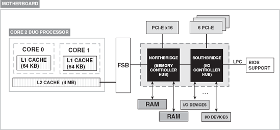
Besides the CPUs, the next most important component of the motherboard is the chipset. The chipset, shown in Figure 2-8, is a group of integrated circuits designed to work together that connects the CPUs to the rest of the components on the motherboard. It is an integrated part of the motherboard and, therefore, cannot be removed or upgraded. It is manufactured to work with a specific class or series of CPUs in order to optimize its performance and the performance of the system in general. The chipset moves data back and forth from CPU to the various components of the motherboard, including memory, graphics card, and I/O devices, as diagrammed in Figure 2-8. All communication to the CPU is routed through the chipset.
The chipset comprises two chips: Northbridge and Southbridge. These names were adopted because of the locations of the chips on the motherboard and the purposes they serve. The Northbridge is located in the northern region, north of many the components on the motherboard, and the Southbridge is located in the southern region, south of some components on the motherboard. Both serve as bridges or connections between devices; they bridge components to make sure that data goes where it is supposed to go.
The Northbridge, also called the memory controller hub, communicates directly with the CPU via the Front Side Bus. It connects the CPUs with high-speed devices such as main memory. It also connects the CPUs with Peripheral Component Interconnect Express (PCI-E) slots and the Southbridge via an internal bus. Data is routed through the Northbridge first before it reaches the Southbridge.
The Southbridge, also called the I/O controller, is a slower than the Northbridge. Because it is not directly connected to the CPUs, it is responsible for the slower capabilities of the motherboard like the I/O devices such as audio, disk interfaces, and so on. The Southbridge is connected to BIOS support via the Serial Peripheral Interface (SPI), six PCI-E slots, and other I/O devices not shown on the diagram. SPI enables the exchange of data (1 bit at a time) between the Southbridge and the BIOS support using a master-slave configuration. It also operates with a full duplex, meaning that data can be transferred in both directions.
PCI-E or PCI Express is a computer expansion card interface. The slot serves as a serial connection for sound, video, and network cards on the motherboard. Serial connections can be slow, sending data 1 bit at a time. The PCI-E is a high-speed serial connection, which works more like a network than a bus. It uses a switch that controls many point-to-point full-duplex (simultaneous communication in both directions) serial connections called lanes. There can be 4, 8, of 16 lanes per slot. Each lane has two pairs of wires from the switch to the device — one pair sends data, and the other pair receives data. This determines the transfer rate of the data. These lanes fan out from the switch directly to the devices where the data is to go. The PCI-E is a replacement of the PCI and provides more bandwidth. Devices do not share bandwidth. The Accelerated Graphics Port (AGP) is replaced with a PCI-E x16 (16 lanes) slot that accommodates more data transferred per second (8 GB/s).
The Core 2 Duo has increased performance of its processor by supporting Streaming SIMD Extensions (SSE) and special registers to perform vectorizable instructions. SSE3 provides a set of 13 instructions that are used to perform SIMD operations on packed integers and floating-point data elements. This speeds up applications that utilize SIMD operations such as highly intensive graphics, encryption, and mathematical applications. The processor has 16 registers used to execute SIMD instructions: 8 MMX and 8 XMM registers. The MMX registers support SIMD operations on 64-bit packed byte, word, and doubleword integers. The XMM data registers and the MXCSR registers support execution of SIMD operations on 128-bit packed single-precision and double-precision floating-point values and 128-bit packed byte, word, doubleword, and quadword integers. Table 2-3 gives a brief description of the three registers, XMM, MMX, MXCSR, involved in executing SIMD operations.
Table 2.3. Table 2-3
Register Set | Description |
|---|---|
MMX | Set of eight registers used to perform operations on 64-bit packed integer data types |
XMM | Set of eight registers used to perform operations on 128-bit packed single- and double-precision floating-point numbers |
MXCSR | Register used with XMM registers for state management instructions |
There are many compiler switches that can be used to activate various capabilities of the multicore processors. For the Intel CC++ compiler, there are compiler switches that activate vectorization options to utilize the SIMD instructions, auto parallelization options, loop unrolling, and code generation optimized for a particular processor.
Although one of the primary jobs of the operating system is to encapsulate the details of the hardware and provide a hardware-independent interface, certain types of developers need to be aware of hardware specifics. These include library developers, compiler designers, system programmers, kernel programmers, server developers, game designers and developers, and others who have maximum system performance as a primary design goal. Four effective yet different designs for multicore architectures are the
Opteron
UltraSparc T1
Cell Broadband Engine
Core 2 Duo
As we have shown, each of these designs has unique features that you as a developer can leverage when you consider programming from a multicore perspective. The C/C++ compiler is the first-level interface to these designs. Homogeneous CMP designs have identical cores. Heterogeneous designs have cores with different instruction sets and architectures. The CBE is a good example of a heterogeneous CMP.
This chapter has now introduced the four architectures that we shall reference throughout this book. All of the code examples have been compiled and tested in one or more of these architectures. Most of the examples have been compiled and tested in all these environments. The program profiles for the program listings contain specific compiler switches and linking options when required. Although each of these architectures is different, we demonstrate methods for dealing with them all in a standard fashion. We want you to be able to take advantage of hardware specifics in the most general way if it's possible. For many software applications, the differences between hardware implementations are hidden because one of the primary design goals is to make the software compatible with as many different hardware platforms as possible. So there is an effort to avoid platform-specific features, as that is one of the primary jobs of the operating system. But with some applications you need to know the specifics of the hardware implementation so that you can optimize the code. Optimization for these applications becomes more important than compatibility. These applications include high-transaction database servers, web servers, application servers, hardware-intensive game engines, compilers, operating system kernels, device drivers, and high-performance scientific modeling and visualization software. Developers of these applications are practically forced to look for and exploit platform features that make their applications acceptable to the end user. So if you are this class of developer, familiarity with a specific processor or family of processors is a prerequisite for effective software development.
In Chapter 3 we turn to the challenges of multicore programming.