
Chapter 2. Getting to Know the Hardware
hard·ware n. The part of a computer system that can be kicked.
As an embedded software engineer, you’ll have the opportunity (and challenge) to work with many different pieces of hardware in your career. In this chapter, we will begin by taking a look at the basics in understanding a schematic. We will also teach you a simple procedure that we use to familiarize ourselves with any new board. In the process, we’ll guide you through the creation of a C-language header file that describes the board’s most important features and a piece of software that initializes the hardware to a known state.
Understanding the Big Picture
Before writing software for an embedded system, you must first be familiar with the hardware on which it will run. At first, you just need to understand the general operation of the system, such as what the board’s main function is and what the inputs and outputs are. Initially, you do not need to understand every little detail of the hardware—how every component or peripheral operates and what registers need to be programmed for particular functions.
Whenever you receive a new board, you should take some time to read the main documents provided with it. If the board is an off-the-shelf product, it might arrive with a “User’s Guide” or “Programmer’s Manual” that has been written for software developers. (The Arcom development kit, for example, includes this information as well as datasheets for all major components on the board.) However, if the board was custom designed for your project, the documentation might be more cryptic or may have been written mainly for the reference of the hardware designers. Either way, this is the single best place to start.
While you are reading the documentation, set the board itself aside. This will help you to focus on the big picture. There will be plenty of time to examine the actual board more closely when you have finished reading. Before picking up the board, you should be able to answer two basic questions about it:
What is the overall purpose of the board?
How does data flow through it?
For example, imagine that you are a software developer on a design team building a print server. You have just received an early prototype board from the hardware designers. The purpose of the board is to share a printer among several computers. The hardware reads data from a network connection and sends that data to a printer for output. The print server must mediate between the computers and decide which computer from the network gets to send data to the printer. Status information also flows in the opposite direction to the computers on the network.
Though the purpose of most systems is self-explanatory, the flow of the data might not be. We often find that a block diagram is helpful in achieving rapid comprehension. If you are lucky, the documentation provided with your hardware will contain a block diagram. However, you might also find it useful to create your own block diagram. That way, you can leave out hardware components that are unrelated to the basic flow of data through the system.
In the case of the Arcom board, the hardware was designed for demonstration purposes rather than with one specific application in mind. However, we’ll imagine that it has a purpose. The user of the device connects the computers to the Ethernet port and a printer to the parallel port. Any computer on the network can then send documents to the printer, though only one of them can do so at a given time.
The diagram in Figure 2-1 illustrates the flow of data through the print server. (Only those hardware devices involved in this application of the Arcom board are shown.) By looking at the block diagram, you should be able to quickly visualize the flow of the data through the system. Data to be printed is accepted from the Ethernet controller, held in RAM until the printer is ready for more data, and delivered to the printer via the parallel port. Status information is fed back to the various computers requesting output on the printer. The software that makes all of this happen is stored in ROM. Note that the PC/104 bus includes buffered signals of the address and data buses in addition to other signals.
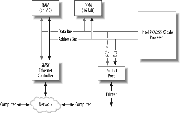
In order to get a better idea of how the block diagram relates to the actual hardware on the Arcom board for our print server device, examine Figure 2-2, which shows the diagram overlaid on top of the Arcom board. This figure gives you a better idea of the ICs involved in the print server device and how the data is routed through the actual hardware.

We recommend creating a project notebook or binder. Once you’ve created a block diagram, place it as the first page in your project notebook. You need it handy so you can refer to it throughout the project. As you continue working with this piece of hardware, write down everything you learn about it in your notebook. If you get a useful handout at a meeting, put it into your notebook. Put tabs in there so you can quickly jump to important information that you refer to all the time. You might also want to keep notes about the software design and implementation. It is very useful to refer back to your notes to refresh your memory about why a particular decision was made for the software. A project notebook is valuable not only while you are developing the software, but also once the project is complete. You will appreciate the extra effort you put into keeping a notebook in case you need to make changes to your software, or work with similar hardware, months or years later.
If you still have any big-picture questions after reading the hardware documents, ask a hardware engineer for some help. If you don’t already know the hardware’s designer, take a few minutes to introduce yourself. If you have some time, take him out to lunch, or buy him a beer after work. (You don’t even have to talk about the project the whole time!) We have found that many software engineers have difficulty communicating with hardware engineers, and vice versa. In embedded systems development, it is especially important that the hardware and software teams be able to communicate with one another. This chapter will give you a solid foundation so that you can speak the language of the hardware engineer.
Before moving on, let’s take a brief detour to better understand the basics of hardware and schematics.
Hardware Basics
The next step in understanding the hardware is to take a look at the schematic. A schematic is a drawing comprised of standardized symbols to represent all of a circuit’s components and connections. The schematic gives the details of the hardware, showing the individual components represented in the block diagram, how the components are interconnected, and, most importantly, where to put the oscilloscope probe to see what’s going on with a particular circuit. On most projects, it is not necessary for you to understand how every electrical circuit on the board operates, but you do need to understand the basic operation of the hardware.
Along with the user’s guides or manuals for the board, it is also helpful to collect the datasheets for all major components on your board. The datasheet is a complete specification of a particular hardware component, including electrical, timing, and interface parameters.
Often the hardware engineer has already collected the datasheets; if so, your work is partly complete. You might want to take a look at the other information available for a particular component, because there are often separate hardware and software documents, especially for more complex devices. For example, a processor often includes a Programmer’s Guide in addition to the other literature. These documents can give you valuable information for using various features of the processor; they occasionally even provide code snippets.
There are also application notes that address particular issues associated with a specific component. It is a good idea to look for any errata documents for all devices. The device’s errata will give you a heads-up on any issues regarding the way a device operates, and, more importantly, workarounds for these issues.
It’s a good idea to periodically check for updates of the board components’ information. This will save you the frustration of chasing a problem that was fixed in the latest datasheet. All of this information is an asset when you are trying to understand a new piece of hardware. You can generally find these documents on the manufacturer’s web site.
Schematic Fundamentals
Before we take a look at a schematic, let’s go over some of the basics of schematics. Figure 2-3 shows some of the basic schematic symbols you will come across, although there might be some variations in symbols from schematic to schematic. The first column gives the name of the particular component; the second column shows the reference designator prefix or component name; and the third column shows the symbols for the related component.
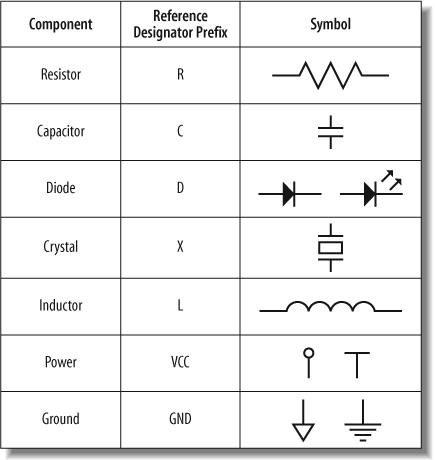
You may notice that two symbols are shown for the diode component. The symbol on the right is for a light emitting diode (LED), which we will take a look at shortly.
The symbols for ground and power can also vary from schematic to schematic; two symbols for power and ground are included in Figure 2-3. In addition to VCC, the reference designator commonly used for power is VDD. Since many circuits use multiple voltage levels, you may also come across power symbols that are labeled with the actual voltage, such as +5 or +3.3, instead of VCC or VDD. The power and ground symbols are typically placed vertically, as shown, whereas the other symbols in Figure 2-3 might show up in any orientation.
A reference designator is a combination of letters, numbers, or both, which are used to identify components on a schematic. Reference designators typically include a number to aid in identifying a specific part in the schematic. For example, three resistors in a schematic might have reference designators R4, R21, and R428. The reference designators are normally silkscreened (a painted overlay) on the circuit board for part identification.
Along with the reference designators, certain components (such as capacitors, inductors, and resistors) are marked by their associated values. For example, in Figure 2-4, resistor R39 has a value of 680 W.
Tip
The values for some components on a schematic are written in a way to aid clarification. For example, a resistor with a value of 4.7 kW has its value written as 4K7. A resistor with a value of 12.4 W is written as 12R4. Using this method, it is easier to understand the value of the component should the decimal fail to print properly.
You will also notice that integrated circuit symbols are not included in this figure. That is because IC schematic representations vary widely. Typically, a hardware engineer needs to create his own schematic symbol for the ICs used in the design. It is then up to the hardware engineer to use the clearest method possible to capture and represent the IC’s symbol.
The reference designator for ICs can vary as well. Typically, the letter U is used. The Arcom board schematic, however, uses the reference designator IC.
IC symbols also include a component type or part number used by the manufacturer. The component type is often helpful when you need to hunt for the datasheets for the parts of a particular design. Descriptive text might save you the trouble of deciphering the markings and codes on the top of a specific IC.
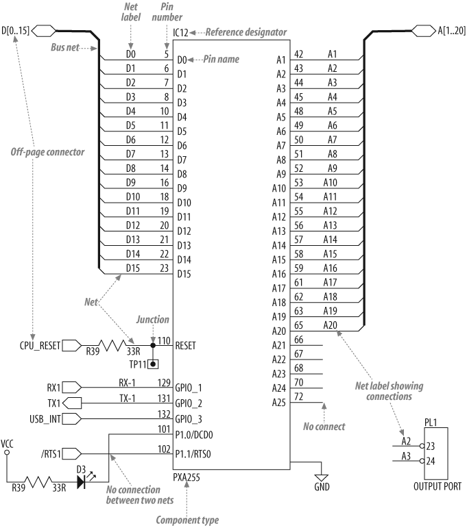
Now that we have an introduction to the symbols used in a schematic, let’s take a look at a schematic. Figure 2-4 is a partial schematic of a fictional board. In this figure, we show some of the connections on the processor.
Tip
The italic labels and associated arrows are not part of the original schematic. These are included to point out particular aspects of the schematic. We wanted to note this because quite often text notes are included in the schematic for clarification or layout concerns. One such clarification note in Figure 2-4 is the label OUTPUT PORT on port PL1.
The processor is the main component in this schematic. The symbol for the processor has a reference designator IC12, which is located at the top of the symbol on this schematic. The component type of the processor is PXA255 and is located at the bottom of the symbol.
The processor’s pins and their associated pin numbers run along the sides of the symbol. For example, bit 0 of the data bus is named D0 and is located on pin number 5 of the processor.
You will also notice that some pins, such as P1.1/rts0 pin number 102, have a bar over the pin name. This indicates that the signal is active low. This means a logic level of 0 will activate the functionality of this signal, whereas a logic level of 1 will deactivate the function. The opposite type of operation is active high.
Active low functionality can also be indicated by a forward slash (/) or tilde (~) placed either before or after the signal name. The signal is then typically pronounced “not RTS0” or “RTS0 bar.” Some component manufacturers represent an active-low signal with the prefix “n” in front of the signal name, such as nRESET.
The wire connecting the different components together is called a net. Two nets that connect create a junction. On the schematic, a junction point is indicated by a dot, as you can see in Figure 2-4 on the RESET pin of the processor. In contrast, when two nets cross, but are not connected, there is no junction. This is shown where the net connected to the LED D3 crosses the net /RTS1.
We say that pins not connected to any nets are no connects or open. No connects are often represented on a schematic with a small cross at the end of the net. Examples of no connect pins are shown on the processor pins A21 through A25. Sometimes IC manufacturers will label no connect pins NC.
Related signals, such as data signals or address signals, are represented on a schematic by a thicker line called a bus net. For example, the data bus is labeled D[0..15] (in other schematics the data bus might be labeled [D0:D15]), which means the data bus net is made up of the signals D0 through D15. The individual signals are shown connecting to the processor data pins. Similarly, the address bus net is labeled A[1..20] and is made up of the signals A1 through A20. Nets connected to a bus net still need to be individually labeled.
If each net in a schematic were connected to the desired location, after a while it could create quite a rat’s nest. [1] Having nets cross over each other is typically avoided in order to maintain clarity in the schematic. To facilitate this clarity, the hardware engineer can use net labels to assign names to the nets. The convention is that nets marked with the same net label are connected, even if the engineer did not actually draw a line connecting them.
For example, in Figure 2-4, a portion of the connector with the reference designator PL1 is shown. (Incidentally, connectors and jumpers often use the reference designator J.) Because the net connected to pin number 23 of the connector PL1 is labeled A2, and the net connected to the processor’s pin number 43 is labeled A2, they are connected even though the hardware engineer did not run a line to represent the A2 net connected from the processor over to PL1.
In order to aid in testing the hardware and software, hardware engineers often include test points. A test point is a metallic area on the finished board that provides access to a particular signal to aid in the debugging or monitoring of that signal. One test point, with the reference designator TP11, is shown in Figure 2-4 on the RESET pin of the processor. With the move to smaller and smaller IC packages and smaller pins, test points are a necessity for debugging and also aid in production testing. Also, it is impossible to probe on any pins of a ball grid array (BGA) package part, because all of the pins are contained under the IC. In this case, a test point helps greatly.
In cases where a schematic cannot fit onto a single page, there must be a way to interconnect nets from one page to another. This is the job of the off-page connector. Off-page connectors can be used for individual nets or bus nets. For example, the off-page connector of the data bus is D[0..15]. This is the exact same off-page connector name used on the memory page to connect the processor’s data bus to the RAM’s data bus.
Tip
We have found a couple of ideas to be useful for off-page connectors. These might be useful mainly for the hardware engineer working on the schematic, but other people on the team should know about them, too.
First, it is helpful if the signal type (input, output, or bidirectional) is properly represented by the appropriate off-page connector. Thus, in Figure 2-4, the data bus off-page connector indicates that these are bidirectional signals; the CPU_RESET off-page connector indicates that this signal is an input to the processor; and the TX1 off-page connector indicates that this signal is an output from the processor.
Another helpful idea is to add a little text note next to each off-page connector with the page number(s) where that particular net is used. This might not make sense for a 5-page schematic, but flipping through 20 pages of schematics can be a nightmare.
Additional tips can be found in the December 2002 Embedded Systems Programming [2] article “Design for Debugability,” which can be found online at http://www.embedded.com.
When you take a look at the full set of schematics, you will notice that there is a block at the lower-righthand corner of each page. This is the title block; every schematic we have come across has some version of this. The title block has useful information about the schematic, such as the date, the designer’s name, the revision, a page number and description of the schematic on that page, and often a list of changes made.
At this point, we have a solid understanding of the system components that make up our platform and how they are interconnected. Let’s next see how to get to know the hardware.
Examine the Landscape
It is often useful to put yourself in the processor’s shoes for a while. Imagine what it is like to be the processor. What does the processor’s world look like? Who is connected to it? How does it talk to these other devices?
If you think about it from this perspective, one thing you quickly realize is that the processor has a lot of compatriots. These are the other pieces of hardware on the board, with which the processor communicates. The processor has different methods for communicating with these other pieces of hardware. In this section, you will learn to recognize their names and addresses.
The first thing to notice is that there are two basic types of hardware to which processors connect: memories and peripherals. Memories are for the storage and retrieval of data and code. Peripherals are specialized hardware devices that either coordinate interaction with the outside world or perform a specific hardware function. For example, two of the most common peripherals in embedded systems are serial ports and timers.
Members of Intel’s 80x86 and some other processor families have two distinct address spaces through which they can communicate with these memories and peripherals. The first address space is called the memory space and is intended mainly for memory devices; the second is reserved exclusively for peripherals and is called the I/O space. However, peripherals can also be located within the memory space, at the discretion of the hardware designer. When that happens, we say that those peripherals are memory-mapped and that system has memory-mapped I/O. Some processors support only a memory space, in which case all peripherals are memory-mapped.
From the processor’s point of view, memory-mapped peripherals look and act very much like memory devices. However, the function of a peripheral is quite different from that of a memory device. Instead of simply storing the data that is provided to it, a peripheral might instead interpret it as a command or as data to be processed in some way.
The designers of embedded hardware often prefer to use memory-mapped I/O exclusively, because it has advantages for both the hardware and software developers. It is attractive to the hardware developer because she might be able to eliminate the I/O space, and some of its associated wires, altogether. This might not significantly lower the production cost of the board, but it might reduce the complexity of the hardware design. Memory-mapped peripherals make life easier for the programmer, who can use C-language pointers, structs, and unions to interact with the peripherals more easily.
Memory Map
All processors store their programs and data in memory. This memory may reside on the same chip as the processor or in external memory chips. Memory is located in the processor’s memory space, and the processor communicates with it by way of two sets of electrical wires called the address bus and the data bus. To read or write a particular location in memory, the processor first writes the desired address onto the address bus. Some logic (either on the processor or in an external circuit), known as an address decoder, interprets the upper address bits on this bus and selects the appropriate memory or peripheral chip. The data is then transferred over the data bus. The address decoder can be an external IC, but today many processors include this logic on-chip.
There are also control signals for reading and writing to various devices in a processor’s memory space that are commonly referred to as the control bus. These control bus signals include read, write, and chip-select (or chip-enable). Some processors combine the read and write signals into a single read/write signal. On these processors, a read operation is performed by setting the signal to one level and a write operation is performed by setting the signal to the opposite level. For example, if the signal name is RD/wr (pronounced “read write bar”), the signal is set to a 1 for a read operation and set to 0 for a write operation.
The chip-select signal is set to its active level when the address for a particular device falls within the device’s address range. For example, let’s say a RAM device occupies the address range from 0x0000 to 0x0FFF. When the software instruction accesses the variable located at address 0x01F2, the chip-select for the RAM is set at its active level.
The read and write signals are set to their active levels by the processor based on the type of memory transaction. Figure 2-5 is an example of a timing diagram, a graphical representation of the timing relationship between the various signals for a given operation. The entire diagram in Figure 2-5 shows one read cycle. In this case, the cycle is reading 16 bits of data from memory. Typically, a table of timing requirements accompanies a timing diagram. The timing requirements detail the minimum and maximum acceptable times for each of the various signals and the timing relationships among the signals.
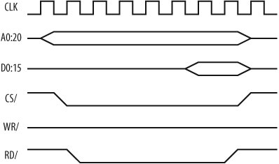
The clock signal (CLK) is the basis for all operations of the processor and is shown as the top signal in the timing diagram of Figure 2-5. The processor clock is generally a square wave that sequences all operations of the processor.
The next group of signals are the address bus, A[0:20], followed by the data bus, D[0:15]. Such buses are depicted in timing diagrams as shown in Figure 2-5, where a single entry represents the entire range of signals rather than each signal having its own entry. A bus is typically stable (meaning it contains a valid address or data) during the period of time when the single line splits into two lines. In hardware terms, the bus goes from being tristate (single line) to having real information present (dual line), and then back to being tristate again.
The next signal is active low chip select (CS/), and after that is the write (WR/) signal, which is also active low. Since this is a timing diagram for a read operation, the write signal stays inactive during the entire cycle. The last signal is the read (RD/). It goes low (active) after the address is set by the processor.
Additional examples of timing diagrams for the PXA255 processor can be found in the Memory Controller section of the PXA255 Processor Developer’s Manual as well as the PXA255 Processor Electrical, Mechanical, and Thermal Specification datasheet.
Tip
Some processors might also include other types of control signals to help access various types of peripheral devices. These signals can be named Ready, Hold, Hold Acknowledge, Wait, and other things. A hardware engineer can use these signals to access a wide range of devices, notably those that operate slower than the processor. For example, a slower ROM can use the processor’s Hold signal to tell the processor it needs more time to complete the read of a particular memory address. The processor can then wait until the ROM is able to finish getting the data for the processor.
While you are reading about a new board, create a table that shows the name and address range of each memory device and peripheral that is located in the memory space. This table is called a memory map. Organize the table so that the lowest address is at the bottom and the highest address is at the top. Each time you add a device to the memory map, place it in its appropriate location in memory and label the starting and ending addresses in hexadecimal. After you have finished inserting all of the devices into the memory map, be sure to label any unused memory regions as such.
If you look back at the block diagram of the Arcom board in Figure 2-1, you will see that there are three devices attached to the address and data buses. (The PC/104 bus is connected to the address and data buses through buffers.) These devices are the RAM, ROM, and SMSC Ethernet controller. The RAM is located at the bottom of the memory address range. The ROM is located toward the top of the range.
Tip
Sometimes a single address range, particularly for memory devices, is comprised of multiple ICs. For example, the hardware engineer might use two ROM chips, each of which has a storage capacity of 1 MB. This gives the processor a total of 2 MB of ROM. Furthermore, the hardware engineer is able to set up the two individual ROM chips so the processor does not know which chip it is actually accessing; the division of the two chips is transparent to the processor, and it sees the memory as one contiguous block.
The memory map in Figure 2-6 shows what the memory devices in Figure 2-1 look like to the processor. Also included in Figure 2-6 are the processor’s internal peripheral registers, labeled PXA255 Peripherals, which are mapped into the processor’s memory space. In a sense, this is the processor’s “address book.” Just as you maintain a list of names and addresses in your personal life, you must maintain a similar list for the processor. The memory map contains one entry for each of the memories and peripherals that are accessible from the processor’s memory space. This diagram is arguably the most important piece of information about the system for an embedded software engineer and should be kept up to date and maintained as part of the permanent records associated with the project.
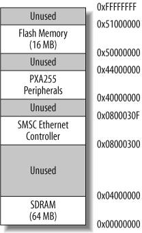
For each new board, you should create a C-language header file that describes its most important features. This file provides an abstract interface to the hardware. In effect, it allows you to refer to the various devices on the board by name rather than by address. This has the added benefit of making your application software more portable. If the memory map ever changes—for example, if the 64 MB of RAM is moved—you need only change the affected lines of the board-specific header file and recompile your application.
Abstracting the hardware into a file (for smaller projects) or a directory of files (for larger projects) also allows you to reuse certain portions of your code as you move from project to project. Because the hardware engineer will likely reuse components in new designs, you too can reuse drivers for these components in these new designs.
As this chapter progresses, we will show you how to create a header file for the Arcom board; the following code is the first section of this file. This part of the header file describes the memory map:
/**********************************************************************
 *
 *  Memory Map
 *
 *            Base Address   Size  Description
 *            -------------- ----- -----------------------------------
 *            0x00000000     64M   SDRAM
 *            0x08000300     N/A   Ethernet controller
 *            0x50000000     16M   Flash
 *
 **********************************************************************/

#define SDRAM_BASE                  (0x00000000)
#define ETHERNET_BASE               (0x08000300)
#define FLASH_BASE                  (0x50000000)
Learn How to Communicate
Now that you know the names and addresses of the memory and peripherals attached to the processor, it is time to learn how to communicate with the peripherals. There are two basic communication techniques: polling and interrupts. In either case, the processor usually issues some sort of command to the device by writing—by way of the memory or I/O space—particular data values to particular addresses within the device, and then waits for the device to complete the assigned task. For example, the processor might ask a timer to count down from 1,000 to 0. Once the countdown begins, the processor is interested in just one thing: is the timer finished counting yet?
If polling is used, the processor repeatedly checks to see whether the task has been completed. This is analogous to the small child who repeatedly asks, “Are we there yet?” throughout a long trip. Like the child, the processor spends a large amount of otherwise useful time asking the question and getting a negative response. To implement polling in software, you need only create a loop that reads the status register of the device in question. Here is an example:
    do
    {
        /* Play games, read, listen to music, etc. */
        ...

        /* Poll to see if we're there yet. */
        status = areWeThereYet();

    } while (status == NO);
The second communication technique uses interrupts. An interrupt is an asynchronous electrical signal from a peripheral to the processor. Interrupts can be generated from peripherals external or internal to the processor, as well as by software.
When interrupts are used, the processor issues commands to the peripheral exactly as before, but then waits for an interrupt to signal completion of the assigned work. While the processor is waiting for the interrupt to arrive, it is free to continue working on other things. When the interrupt signal is asserted, the processor finishes its current instruction, temporarily sets aside its current work, and executes a small piece of software called the interrupt service routine (ISR) or interrupt handler. When the ISR completes, the processor returns to the work that was interrupted.
Of course, this isn’t all automatic. The programmer must write the ISR himself and “install” and enable it so that it will be executed when the relevant interrupt occurs. The first few times you do this, it will be a significant challenge. But, even so, the use of interrupts generally decreases the complexity of one’s overall code by giving it a better structure. Rather than device polling being embedded within an unrelated part of the program, the two pieces of code remain appropriately separate.
On the whole, interrupts are a much more efficient use of the processor than polling. The processor is able to use a larger percentage of its waiting time performing useful work. However, there is some overhead associated with each interrupt. It takes a good bit of time—relative to the length of time it takes to execute an opcode—to put aside the processor’s current work and transfer control to the interrupt service routine. Many of the processor’s registers must be saved in memory.
In practice, both interrupts and polling are used frequently. Interrupts are used when efficiency is paramount or when multiple devices must be monitored simultaneously. Polling is typically used when the processor must respond to some event more quickly than is possible using interrupts or when large amounts of data are expected to arrive at particular intervals, such as during real-time data acquisition. We will take a closer look at interrupts in Chapter 8.
Getting to Know the Processor
If you haven’t worked with the processor on your board before, you should take some time to get familiar with it now. This shouldn’t take very long if you do all of your programming in a high-level language such as C. You need to dig in and find out how particular peripherals of the processor work. Generally, to the user of a high-level language, most processors look and act pretty much the same. However, if you’ll be doing any assembly language programming, you need to familiarize yourself with the processor’s register architecture and instruction set.
Everything you need to know about the processor can be found in the databooks provided by the manufacturer. If you don’t have a databook or programmer’s guide for your processor already, you should obtain one immediately. If you are going to be a successful embedded systems programmer, you must be able to read databooks and get something out of them. Processor databooks are usually well written—as databooks go—so they are an ideal place to start. Begin by flipping through the databook and noting sections that are most relevant to the tasks at hand. Then go back and begin reading the processor overview section.
Things you’ll want to learn about the processor from its databook are:
What address does the processor jump to after a reset?
What is the state of the processor’s registers and peripherals at reset?
What is the proper sequence to program a peripheral’s registers?
Where should the interrupt vector table be located? Does it have to be located at a specific address in memory? If not, how does the processor know where to find it?
What is the format of the interrupt vector table? Is it just a table of pointers to ISR functions?
Are there any special interrupts—sometimes called traps—that are generated within the processor itself? Must an ISR be written to handle each of these?
How are interrupts enabled and disabled? Globally and individually?
How are interrupts acknowledged or cleared?
In addition to the processor databook, the Internet contains a wealth of information for embedded software developers. The manufacturer’s site is a great place to start. In addition, a search for a particular processor can yield oodles of useful information from fellow developers, including code snippets giving you exact details on how to write your software. Several newsgroups are also targeted toward embedded software development and toward specific processors.
Warning
You need to take care to fully understand any licensing issues of the software you find on the Internet should you decide to use someone else’s code. You might have to get your company’s legal department involved in order to avoid any problems.
Another useful tool for understanding the processor is a development board. Once the processor is selected, you can search for your options for a development board. You need to consider the peripherals and software tools included on the development board. For example, if your application is going to include an Ethernet port, it would be a good idea to select a development board that also includes an Ethernet port. There is typically example software included with the development board as well. If the project uses a processor that you have not worked with before, the example software can get you up the learning curve a lot faster. The development board will assist you in getting a jump-start on the embedded software development.
Another benefit of a development board is that if you are seeing some oddities related to your project’s hardware, you can always go back to the development board (where the hardware should be stable) and run some tests to see whether the problem is specific to the new design.
Processors in General
Many of the most common processors are members of families of related devices. In some cases, the members of such a processor family represent points along an evolutionary path. The most obvious example is Intel’s 80x86 family, which spans from the original 8086 to the Pentium 4 and beyond. In fact, the 80x86 family has been so successful that it has spawned an entire industry of imitators.
As it is used in this book, the term processor refers to any of three types of devices known as microprocessors, microcontrollers, and digital signal processors. The name microprocessor is usually reserved for a chip that contains a powerful central processing unit (CPU) that has not been designed with any particular computation in mind. These chips are usually the foundation of personal computers and high-end workstations, although microprocessors are used in embedded systems as well. Other widely known microprocessors are members of Freescale’s [3] 68K—found in older Macintosh computers—and the ubiquitous 80x86 families.
A microcontroller is very much like a microprocessor, except that it has been designed specifically for use in embedded systems. Microcontrollers typically include a CPU, memory (a small amount of RAM, ROM, or both), and other peripherals in the same integrated circuit. If you purchase all of these items on a single chip, it is possible to reduce the cost of an embedded system substantially. Among the most popular microcontrollers are the 8051 and its many imitators and the 68HCxx series. It is also common to find microcontroller versions of popular microprocessors. For example, Intel’s 386 EX is a microcontroller version of the 80386 microprocessor.
The final type of processor is a digital signal processor, or DSP. The CPU within a DSP is specially designed to perform discrete-time signal processing calculations—like those required for audio and video communications—extremely fast. Because DSPs can perform these types of calculations much faster than other processors, they offer a powerful, low-cost microprocessor alternative for designers of cell phones and other telecommunications and multimedia equipment. Analog Devices, Freescale, and TI are each vendors of common DSP devices.
The PXA255 XScale Processor
The processor on the Arcom board is a PXA255 that incorporates the XScale core. XScale is based on the ARM Version 5TE architecture. In order to find out more about the ARM processor, a great book is David Seal’s ARM Architecture Reference Manual (Addison-Wesley); this book is commonly referred to as the “ARM ARM.”
In addition to the CPU, the PXA255 contains an interrupt control unit, a memory controller, several general-purpose I/O pins, four timer/counters, an I2C bus interface unit, four serial ports, 16 direct memory access (DMA) channels, a memory controller that supports several memory types including DRAM, a USB client, an LCD controller, two pulse width modulators, a real-time clock, a watchdog timer unit, and a power management unit. These extra hardware devices are located within the same chip and are referred to as on-chip peripherals. The CPU is able to communicate with and control the on-chip peripherals directly, via internal buses.
Although the on-chip peripherals are distinct hardware devices, they act like little extensions of the PXA255 CPU. The software can control them by reading and writing to the peripheral specific registers. The control and status registers for each of the on-chip peripherals are located at fixed addresses in memory space. The exact addresses of each register can be found in the PXA255 Processor Developer’s Manual. To isolate these details from your application software and to aid in the readability of your software, it is good practice to include the addresses of any registers you will be using in the header file for your board. You can see from the following code snippet that it is more difficult to understand what is going on when addresses are used directly:
if (bLedEnable == TRUE)
{
    *((uint32_t *)0x40E00018) = 0x00400000;
}
Although comments could clarify what is going on in the above code, it is better to use more descriptive names in your software that will make your code self-documenting, but do add comments as well to aid in understanding.
In addition to a header file describing the board’s features, a C-language header file that describes the processor’s registers should also be created. An example of descriptive names for some of the registers in the PXA255 processor follows. It is also helpful to define descriptive names for particular bits in a register if they will be addressed individually. [4]
/********************************************************
 * PXA255 XScale ARM Processor On-Chip Peripherals
 ********************************************************/

/* Timer Registers */
#define TIMER_0_MATCH_REG           (*((uint32_t volatile *)0x40A00000))
#define TIMER_1_MATCH_REG           (*((uint32_t volatile *)0x40A00004))
#define TIMER_2_MATCH_REG           (*((uint32_t volatile *)0x40A00008))
#define TIMER_3_MATCH_REG           (*((uint32_t volatile *)0x40A0000C))
#define TIMER_COUNT_REG             (*((uint32_t volatile *)0x40A00010))
#define TIMER_STATUS_REG            (*((uint32_t volatile *)0x40A00014))
#define TIMER_INT_ENABLE_REG        (*((uint32_t volatile *)0x40A0001C))

/* Timer Interrupt Enable Register Bit Descriptions */
#define TIMER_0_INTEN               (0x01)
#define TIMER_1_INTEN               (0x02)
#define TIMER_2_INTEN               (0x04)
#define TIMER_3_INTEN               (0x08)

/* Timer Status Register Bit Descriptions */
#define TIMER_0_MATCH               (0x01)
#define TIMER_1_MATCH               (0x02)
#define TIMER_2_MATCH               (0x04)
#define TIMER_3_MATCH               (0x08)

/* Interrupt Controller Registers */
#define INTERRUPT_PENDING_REG       (*((uint32_t volatile *)0x40D00000))
#define INTERRUPT_ENABLE_REG        (*((uint32_t volatile *)0x40D00004))
#define INTERRUPT_TYPE_REG          (*((uint32_t volatile *)0x40D00008))

/* Interrupt Enable Register Bit Descriptions */
#define GPIO_0_ENABLE               (0x00000100)
#define UART_ENABLE                 (0x00400000)
#define TIMER_0_ENABLE              (0x04000000)
#define TIMER_1_ENABLE              (0x08000000)
#define TIMER_2_ENABLE              (0x10000000)
#define TIMER_3_ENABLE              (0x20000000)

/* General Purpose I/O (GPIO) Registers */
#define GPIO_0_LEVEL_REG            (*((uint32_t volatile *)0x40E00000))
#define GPIO_1_LEVEL_REG            (*((uint32_t volatile *)0x40E00004))
#define GPIO_2_LEVEL_REG            (*((uint32_t volatile *)0x40E00008))
#define GPIO_0_DIRECTION_REG        (*((uint32_t volatile *)0x40E0000C))
#define GPIO_1_DIRECTION_REG        (*((uint32_t volatile *)0x40E00010))
#define GPIO_2_DIRECTION_REG        (*((uint32_t volatile *)0x40E00014))
#define GPIO_0_SET_REG              (*((uint32_t volatile *)0x40E00018))
#define GPIO_1_SET_REG              (*((uint32_t volatile *)0x40E0001C))
#define GPIO_2_SET_REG              (*((uint32_t volatile *)0x40E00020))
#define GPIO_0_CLEAR_REG            (*((uint32_t volatile *)0x40E00024))
#define GPIO_1_CLEAR_REG            (*((uint32_t volatile *)0x40E00028))
#define GPIO_2_CLEAR_REG            (*((uint32_t volatile *)0x40E0002C))
#define GPIO_0_FUNC_LO_REG          (*((uint32_t volatile *)0x40E00054))
#define GPIO_0_FUNC_HI_REG          (*((uint32_t volatile *)0x40E00058))
Let’s take a look at the earlier code snippet written to use a register definition from the example header file:
if (bLedEnable == TRUE)
{
    GPIO_0_SET_REG = 0x00400000;
}
This code is a lot easier to read and understand, even without a comment. Defining registers in a header file, as we have shown in the preceding code, also prevents you or another team member from running to the databook every other minute to look up a register address.
Study the External Peripherals
At this point, you’ve studied every aspect of the new hardware except the external peripherals. These are the hardware devices that reside outside the processor chip and communicate with it by way of interrupts and I/O or memory-mapped registers.
Begin by making a list of the external peripherals. Depending on your application, this list might include LCD or keyboard controllers, analog-to-digital (A/D) converters, network interface chips, or custom application-specific integrated circuits (ASICs). In the case of the Arcom board, the list contains just two items: the SMSC Ethernet controller and the parallel port.
You should obtain a copy of the user’s manual or datasheet for each device on your list. At this early stage of the project, your goal in reading these documents is to understand the basic functions of the device. What does the device do? What registers are used to issue commands and receive the results? What do the various bits and larger fields within these registers mean? When, if ever, does the device generate interrupts? How are interrupts acknowledged or cleared at the device?
When you are designing the embedded software, you should try to break the program down along device lines. It is usually a good idea to associate a software module called a device driver with each of the external peripherals. A device driver is nothing more than a collection of software routines that control the operation of a specific peripheral and isolate the application software from the details of that particular hardware device. We’ll have a lot more to say about device drivers later on.
Initialize the Hardware
The final step in getting to know your new hardware is to write some initialization software. This is your best opportunity to develop a close working relationship with the hardware, especially if you will be developing the remainder of the software in a high-level language.
During hardware initialization, it may be impossible to avoid using assembly language. However, after completing this step, you will be ready to begin writing small programs. [5]
Tip
If you are one of the first software engineers to work with a new board—especially a prototype—the hardware might not work as advertised. All processor-based boards require some amount of software testing to confirm the correctness of the hardware design and the proper functioning of the various peripherals. This puts you in an awkward position when something is not working properly. How do you know whether the hardware or your software is causing the problem? If you happen to be good with hardware or have access to a simulator, you might be able to construct some experiments to answer this question. Otherwise, you should probably ask a hardware engineer to join you in the lab for a joint debugging session.
The hardware initialization should be executed before the
startup code described in Chapter 4. The code
described there assumes that the hardware has already been initialized
and concerns itself only with creating a proper runtime environment for
high-level language programs. Figure 2-7 provides an
overview of the entire initialization process, from processor reset
through hardware initialization and C startup code to main.
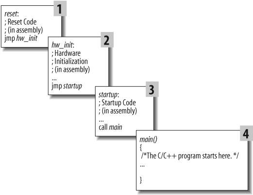
The first stage of the initialization process is the reset code. This is a small piece of assembly language (usually only two or three instructions) that the processor executes immediately after it is powered on or reset. The sole purpose of this code is to transfer control to the hardware initialization routine. The first instruction of the reset code must be placed at a specific location in memory, usually called the reset address or reset vector, which is specified in the processor databook. The reset address for the PXA255 is 0x00000000.
Most of the actual hardware initialization takes place in the second stage.
At this point, we need to inform the processor about its environment.
This is also a good place to initialize the interrupt controller and
other critical peripherals. Less critical hardware devices can be
initialized when the associated device driver is started, usually from
within main.
The PXA255 has boot select pins that allow you to specify the type and width of the memory device from which the processor attempts to execute the initial instructions. The memory device that the processor boots from typically contains the code to program several internal registers of the PXA255 that must be programmed before any useful work can be done with the processor. These internal registers are responsible for setting up the memory map and are part of the processor’s internal memory controller. By programming the memory interface configuration registers, you are essentially waking up each of the memory and peripheral devices that are connected to the processor.
The PXA255 contains six chip-selects for interfacing to various types of external memory. These chip-selects are active for accesses in particular memory ranges. Each chip-select is associated with a single “chip enable” wire that runs from the processor to some other chip. In many systems, the circuitry to do this is external to the processor. The association between particular chip-selects and hardware devices must be established by the hardware designer. All you need to do is get a list of chip-select settings from her and load those settings into the memory configuration registers.
Upon reset, the PXA255 jumps to the address 0x00000000, which activates chip select 0 (the nCS[0] pin). This is the processor’s “fetal position,” and it implies that this chip-select is used to access some type of nonvolatile memory, such as flash in the Arcom board’s case. Since there are no other chip-selects configured at this point, the software must also not require the use of any RAM. This includes making a subroutine call, as this will require access to the stack (discussed in a moment), which lives in RAM; function calls are verboten. Until the RAM is active and the stack pointer initialized, your code must be linear.
The hardware initialization routine, hw_init, should start by initializing the
memory interface configuration registers to inform the processor about
the other memory and peripheral devices that are installed on the board.
By the time this task is complete, the entire range of ROM and RAM addresses will be enabled, so the remainder of
your software can be located at any convenient address in either ROM or
RAM.
The third initialization stage contains the startup code. Its job is to prepare
the way for code written in a high-level language. One of the important
tasks of this code is to set up the stack for the system. The
stack is the area of RAM that the processor
uses for temporary storage during execution. The stack operates on the
last-in-first-out (LIFO) principle in which
items of data are pushed onto and popped off of the stack: typically,
local variables (a.k.a. automatic variables) and return addresses from
function calls during program execution. After initializing the stack,
the startup code calls main. From that point forward, all of your other
software can be written in a high-level language.
Hopefully, you are starting to understand how embedded software gets from processor reset to your main program. Admittedly, the very first time you try to pull all of these components (reset code, hardware initialization, high-level language startup code, and application) together on a new board, there will be problems. So expect to spend some time debugging each of them. We’ll take a look at debugging in Chapter 5.
With a new hardware platform, some hardware problems may pop up as well. These might lead to a problem where the processor simply doesn’t do anything. Sometimes the problem is a basic issue that was overlooked. Some of the basic things to do are:
Make sure the processor and ROM are receiving the proper voltage required to operate the parts.
Check to make sure the clock signal is running. The processor won’t do anything without a clock.
Verify that the processor is coming out of reset properly. You can check the address a processor is fetching using a logic analyzer. This will validate that the processor is trying to fetch the first instruction from the location you expect.
Make sure that a watchdog timer isn’t resetting the processor.
Ensure that input pins on the processor are pulled high or low. This is particularly important for interrupt pins. An input pin in an unknown state (commonly called a floating pin) can wreak all sorts of havoc for a processor.
The hardware engineer might handle these tasks for you, but don’t be afraid to jump right in and look over the schematics yourself. Or better yet, see whether you can sit in the lab with the hardware engineer while he performs his initial checkout of the board.
Expect that the initial hardware bring-up will be the hardest part of the project. You will soon see that once you have a basic program operating that you can fall back on, the work just gets easier and easier—or at least more similar to other types of computer programming.
[1] Incidentally, “rats nest” is the term used to describe the connection of nets made during layout. Once you see the initial stage of a layout, you’ll understand how this name was derived.
[2] Embedded Systems Programming magazine has changed its name to Embedded Systems Design.
[3] This is Motorola’s new semiconductor division.
[5] In order to make the example in Chapter 3 a little easier to understand, we didn’t show any of the initialization code there. However, it is necessary to get the hardware initialization code working before you can write even simple programs such as Blinking LED. The Arcom board includes a debug monitor that handles all of the assembly language hardware initialization.